Tunnel Diode Loaded Microstrip Antenna with Parasitic
Elements
Rakesh N. Tiwari1, Prabhakar Singh2
1Department of Electronics and Communication Engineering, Raffles University, Neemrana, India; 2Department of Physics,
Galgo-tias University, Greater Noida, India. Email: [email protected]
Received January 20th,2012; revised February 16th, 2012; accepted March 15th, 2012
ABSTRACT
The present work describes the circuit model based analysis of symmetrically tunnel diode loaded microstrip antenna with parasitic elements. To optimize the antenna characteristics, a systematic study has been carried out as a function of tunnel diode bias voltage, space between parasitic patch and fed patch. The results obtained from antenna radiation pat-tern depict that an improvement of 5.8 MHz in bandwidth can be achieved if the symmetrically tunnel diode is loaded with patch along with parasitic elements of gap (s) = 3.6 cm. It has also been noted that at this state the radiations are more powerful i.e. 0.5647 dB as compared to single patch design.
Keywords: Microstrip Antenna; Symmetrically Tunnel Diode Loaded Patch and Parasitic Patch
1. Introduction
Microstrip patch antennas have attracted widespread interest due to their small size, light weight, low profile and low cost as well as to the fact that they are easy to manufacture, suitable to planar and non planar surfaces, mechanically robust, easily integrated with circuits but their narrow bandwidth and low gain make these antennas for limited use [1,2]. In the multi-channel application a small instantaneous bandwidth is required over a large frequency range. A tunable microstrip antenna provides an alternative to wideband operation in which an antenna with small bandwidth is tuned over a large frequency band [3]. Active device loaded patch is widely used to make a tunable antenna [4]. Several researchers have used parasitic elements along the radiating and non- radiating edges of the fed patch to achieve additional gain [5].
In the present paper the radiation characteristics and resonance behavior of the symmetrically tunnel diode loaded microstrip antenna with parasitic elements at radiating edges has been studied by using circuit model approach for the first time. Consequently various antenna parameters such as input impedance, VSWR, return losses etc. are evaluated as a function of frequency for different bias voltages. The effect of separation (s) be- tween the patch and parasitic elements is also inves- tigated for different bias voltages.
2. Antenna Geometry and Its Equivalent
Circuit
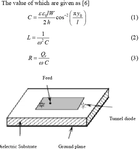
[image:1.595.315.540.462.702.2]Tunnel diode loaded microstrip antenna is shown in
Figure 1, in which rectangular microstrip antenna
(RMSA) is considered as a parallel combination of R, L and C.
The value of which are given as [6]
2
0 cos π
2
lW y
C
h l
0
(1)
2
1
L C
(2)
r
Q R
C
(3)
Ground plane Dielectric Substrate
Tunnel diode Feed
where
4
e r
c Q
f h
here, e is effective permittivity of the medium which is
given by [6].
1 2
1 1 10
1
2 2
r r
e
h W
(4) where c is the velocity of light, f is the design frequency,
e
is the relative permittivity of the substrate material, and W are length and width of the rectangular patch and h is thickness of the substrate material. yo is
Y-coordinate of the feed point. The equivalent circuit of the tunnel diode is shown in Figure 2, in which Rs is
resistance, Ls is inductance, –RD is negative resistance
and CD is the junction capacitance [7].
l
The junction capacitance CD is given as
1 2
1 2
2 D
q n p
C A V V
n p
d b (5)
The impedance of symmetrically tunnel loaded patch can be given as in Figure 3.
2.1. Symmetrically Tunnel Diode Loaded Patch with Parasitic Elements
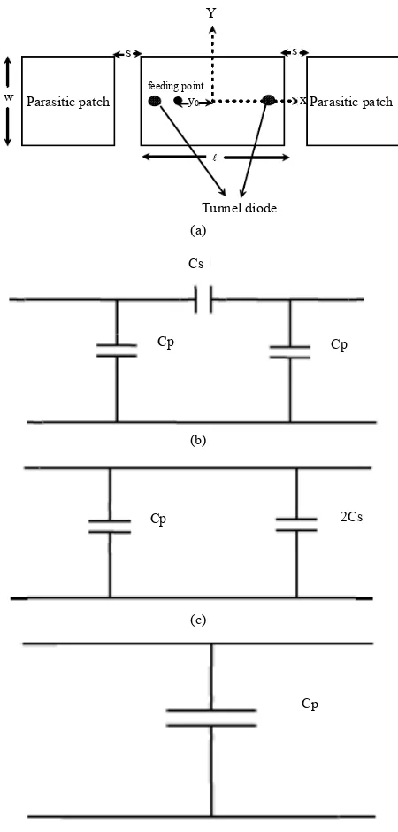
Figure 4(a) shows two parasitic elements placed at the
radiating edges of the RMSA with separation (s) and width W. The equivalent circuit of parasitic elements is shown in Figure 4(b). It may be mentioned that such
circuit can be analyses using odd and even mode concept
–RD CD
LS
[image:2.595.311.536.221.691.2]RS
Figure 2. Equivalent circuit of tunnel diode.
–RD CD
LS
RS
–RD
RS LS
R L C
CD
Figure 3. Equivalent circuit of symmetrically tunnel inte- grated RMSA.
and hence equivalent circuit of the odd and even mode can be written as shown in Figures 4(c) and (d) res-
pectively.
Now the combined equivalent circuit of tunnel loaded patch with parasitic elements can be given as shown in
Figures 5(a) and (b) for odd and even mode cases.
2.2. Operating Frequency
The operating frequency range of the tunnel diode oscillator controlled by self resonance frequency
fsTunnel diode Y
s
w Parasitic patch feeding point Parasitic patch
x y0
s
(a)
Cp Cs
Cp
(b)
Cp 2Cs
(c)
Cp
(d)
[image:2.595.59.288.485.712.2]
2 2
1 2 2
2
D s s D D s s
D S s
c RLC R RR C C L C R L
C L R R
2Cs 2Cs Cp
Cp z
2 2 D s s D D s
c C L R RL C C LC L
3 s
c R R
(a)
1 2 s
d R RL
2Cp
2Cp z d22R RC LLs D s
Now the combined equivalent circuit of tunnel loaded patch with parasitic elements can be given as shown in
Figures 5(a) and (b) for odd and even mode cases. From Figure 3, the impedance of symmetrically tunnel loaded
patch can be given as
(b)
Figure 5. (a) Odd mode; (b) Even mode. Equivalent circuit of symmetrically tunnel loaded RMSA with parasitic ele-
ments. Z
Z1Z2
Z3 (10) whereand resistive cut off frequency
fr whose values aregiven by [8]. Z1Rs j L s
1
2π
D D s
s
D D s
C R L
f
C R L
(6) 2
1 D D D
R Z
j C R
1
2π
D s
r
D D s
R R
f
C R R
(7) 3 1
2
D
D D D
j LRR
Z Z
j L R R RR RLR C CD
From Figure 5, the equivalent circuit for tunnel loaded
patch with parasitic elements can be used to calculate odd and even mode impedances. The odd mode capa- citance
C0 and even mode capacitance can begiven as [8].
eC When the negative resistance of the tunnel diode goes
to zero then the oscillation ceases to exist. Thus the resistive cut off frequency indicates that operating frequency should be less than fr. The equivalent circuit of
symmetrically tunnel loaded RMSA can be given as shown in Figure 3. The condition for oscillation of
tunnel loaded patch is [7] C0 Cp 2Cs
(11) 2
e
C Cp (12)
Im Y 0 (8)
From Figure 5, the impedances for odd and even
mode can be given as where Y is the admittance of the circuit as seen by the
negative resistance –RD. From Figure 3, we can evaluate
imaginary part of admittance as Equation (9) and Z0 Z 4Xs 2Xp (13) where
4
e p
Z Z X (14)
2
1 s D s 2 s
a RL LR R C R L
where Xs and Xp are capacitive impedances of gap
and parasitic elements.
2 2
2
2
2 2
D s D D s s
D s s s D
a RLC L RL C C C R L
LC L R L C R
Total input impedance of the symmetrically tunnel loaded RMSA with parasitic elements is given by
3 D s D
a RLC L C C ZT Z0Ze (15)
The different antenna parameters can be calculated as Reflection coefficient
2 1 s D
b L C RL
C TC T
Z Z
Z Z
(16)
2
2 D s 2 s
b RL C R L
2 3 4 2 2 4
1 2 2 1 2 1 2 3 1 2
2
4 2 2 2
1 2 1 2
Im Y a a a b b c c c d d
b b d d
2
[image:3.595.309.535.265.384.2] [image:3.595.115.253.319.383.2]where ZC is the characteristic impedance of the coaxial
feed (50 Ω).
1 1
VSWR
(17)
2
1 Return loss 10log
(18)
The radiation pattern for tunnel loaded RMSA with parasitic elements can be calculated as
tp t
E AF E (19)
tp t
E AF E (20) where AF is array factor and given by [10].
2.3. Design Specifications for Microstrip Patch Antenna
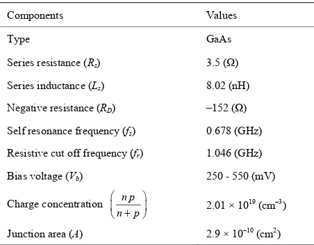
The designed frequency of the rectangular patch antenna is 1 GHz. The dimension of the rectangular patch is calculated by [6]. The detail design specifications are given in Table 1 and Table 2.
3. Result and Discussion
[image:4.595.310.533.351.512.2]Variation of return loss for single patch, tunnel diode
Table 1. Design specifications for the tunnel diode.
Components Values
Type GaAs
Series resistance (Rs) 3.5 (Ω)
Series inductance (Ls) 8.02 (nH)
Negative resistance (RD) –152 (Ω)
Self resonance frequency (fs) 0.678 (GHz)
Resistive cut off frequency (fr) 1.046 (GHz)
Bias voltage (Vb) 250 - 550 (mV)
Charge concentration n p
n p
2.01 × 10
19 (cm–3)
Junction area (A) 2.9 × 10⁻¹⁰ (cm2)
Table 2. Design specifications for microstrip patch antenna.
Components Values
Substrate material used Bakelite
Relative dielectric constant (εr) 4.78
Thickness of the substrate (h) 0.159 (cm)
Design frequency (f) 1.0 (GHz)
Length of the patch (l) 6.8108 (cm)
Width of the patch (W) 8.8083 (cm)
loaded patch and tunnel loaded patch with parasitic ele- ments are shown in Figure 6, for different values of bias
voltages. It is observed that the resonance occurs for tun- nel loaded patch at lower value as compared to single patch and it is still lower for parasitic loaded patch for all the values of bias voltage.
From Figure 7, it is also observed that the bandwidth
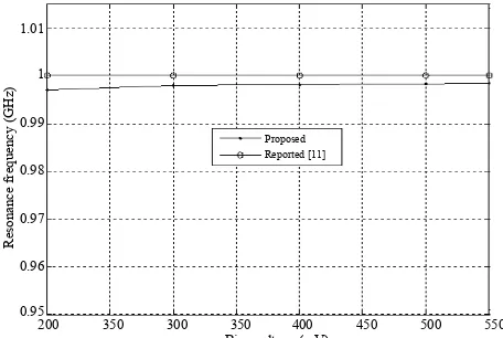
of the patch improves by loading the patch with tunnel diodes. However, by loading the tunnel loaded patch with parasitic elements the bandwidth further improves as compared to patch. Typically it may be noted that maximum bandwidth is achieved for tunnel loaded patch with parasitic element having s = 3.6 cm. When the value of (s) increases bandwidth decreases. At s = 9.9 cm, the antenna behaves as a tunnel loaded patch and the effect of parasitic elements ceases to exist. This is because of the fact that when (s) is more than 9.6 cm. there is no coupling between patch and parasitic elements. Variation of resonance frequency with bias voltage is shown in
Figure 8. It is found that the resonance frequency in-
creases minutely with bias voltage. The result is in good
0.995 0.996 0.997 0.998 0.999 1 1.001 1.002 1.003
patch
tunnel loaded patch, vb=250Mv tunnel loaded patch, vb=350mV tunnel loaded patch, vb=450mV tunnel loaded patch, vb=550mV s = 3.6 cm,vb = 250 mV s = 3.6 cm,vb = 350 mV s = 3.6 cm,vb = 450 mV s = 3.6 cm,vb = 550 mV
0
–5
–10
–15
–20
–25
–30
–35
–40
Frequency (GHz)
Retur
[image:4.595.59.285.418.594.2]n loss (db)
Figure 6. Variation of return loss with frequency for dif- ferent bias voltage.
0.995 0.996 0.997 0.998 0.999 1 1.001 1.002 1.003
tunnel loaded patch s = 3.6 cm s = 6.6 cm s = 8.6 cm s = 9.6 cm s = 9.9 cm
–2
–4
–6
–8
–10
–12
–14
–16
–18
Frequency (GHz)
Retu
rn lo
ss
(d
[image:4.595.311.536.555.706.2]b)
[image:4.595.59.286.622.737.2]agreement with the reported data [10]. The radiation pat- tern of the antenna is shown in Figure 9. It is observed
that tunnel loaded patch with parasitic elements for (s) = 3.6 cm shows maximum radiated power which is 0.5647 dB higher as compared to patch alone. It is further noted that the radiation pattern is invariant with the bias volt- age.
4. Conclusion
It is concluded from the above analysis that the band- width of the tunnel loaded patch antenna with parasitic
200 350 300 350 400 450 500 550
Proposed Reported [11]
1.01
1
0.99
0.98
0.97
0.96
0.95
Bias voltage (mV)
R
es
ona
nc
e f
re
que
nc
y
(G
Hz
[image:5.595.57.285.236.389.2])
Figure 8. Variation of resonance frequency with bias vol- tage.
–80 –60 –40 –20 0 20 40 60 80
tunnel loaded patch, s = 3.6 cm, vb=550mV patch
0
–2
–4
–6
–8
–10
–12
Angle (degree)
R
el
at
ive
R
ad
at
ed
P
ow
er
(d
B
[image:5.595.62.284.431.588.2])
Figure 9. Radiation pattern of the tunnel diode loaded patch antenna with parasitic elements.
elements is improved and it is found maximum for the patch size (s) = 3.6 cm. Further, an increase in gap (s) (beyond s = 9.9 cm) reduces the bandwidth. It means the effect of tunnel loaded patch and the parasitic elements ceases to exist or at this state the effective mutual inter-action between patch and parasitic elements is stopped. In this way the performance of tunnel diode loaded mi-crostrip antenna can be enhanced by using parasitic ele-ments of optimum gap (s).
REFERENCES
[1] K. R. Carver and J. W. Mink, “Microstrip Antenna Technology,” IEEE Transactions on Antennas and Pro- pagation, Vol. 29, No. 1, 1981, pp. 2-24.
doi:10.1109/TAP.1981.1142523
[2] D. M. Pozar, “An Update on Microstrip Antenna Theory and Design Including Some Novel Feeding Techniques,”
IEEE Antennas and Propagation Society Newsletter, Vol. 28, No. 5, 1986, pp. 4-9.
[3] J. A. Ansari,R. B. Ram, S. K. Dubey and P. Singh, “A Frequency Agile Stacked Annular Ring Microstrip An-tenna Using Gunn Diode,” Smart Materials and Structures, Vol. 16, No. 6, 2007, pp. 2040-2045.
doi:10.1088/0964-1726/16/6/006
[4] P. Bhartia and I. J. Bahal, “Frequency Agile Microstrip Antennas,” Microwave Journal, Vol. 25, No. 10, 1982, pp. 67-70.
[5] G. Kumar and K. C. Gupta, “Broad-Band Microstrip An-tennas Using Additional Resonators Gap-Coupled to the Radiating Edges,” IEEE Transactions on Antennas and Propagation, Vol. 32, No. 12, 1984, pp. 1375-1379. doi:10.1109/TAP.1984.1143264
[6] I. J. Bahl and P. Bhartia, “Microstrip Antennas,” Artech House, Dedham, 1981.
[7] W. F. Woo and. F. Chow, “Principles of Tunnel Diode Circuits,” Wiley, New York, 1969.
[8] S. P. Sylvesten and P. Gentile, “Basic Tunnel Theory and Application of Tunnel Diode,” D. Van Nostrand, Princeton, 1962.
[9] R. Garg and I. J. Bahal, “Microstrip Discounties,” Inter-national Journal of Electronics, Vol. 45, No. 12, 1978, pp. 81-87. doi:10.1080/00207217808900883