MIRZAEE TESHNIZI, HESAMEDDIN. Medium-Voltage DC Power Conversion and Distribution for Efficient Electric Power Delivery in Shipboard and Mobile Mining Application. (Under the direction of Dr. Subhashish Bhattacharya).
Medium-Voltage DC (MVDC) distribution and power conversion systems have become more attractive in recent years due to advances in power electronic technology. It can be used in a range of high power applications such as shipboard, electric propulsion in large multi-motor drives, and so on.
In this dissertation, first, the concept of a MVDC amplifier system for shipboard application is proposed. The dc amplifier system must provide a medium-voltage dc bus with the possibility of superposing a high bandwidth time-varying signal and should be capable of producing voltage excursions at a high slew-rate. This is intended to facilitate the development of new technologies, i.e., new high power non-linear loads based on power electronics, in all electric ships as part of the newly proposed MVDC ship power system. To achieve the required system characteristics, a specific ‘hybrid front-end’ is proposed in which a high-power, line-commutated multi-pulse thyristor-based front-end, which serves as the main AC-to-DC converter, is integrated with an IGBT-based DC active power filter (SDAF) connected in series on DC-bus. The system parameters and specifications for the MVDC amplifier system are set forth, and the proposed system solution is validated through both simulations and experimental results based on a 12-kVA, 400-V laboratory-scale DC amplifier test-bed.
diode-towards a simpler, more efficient and more reliable system. In this hybrid circuit topology, a 12-pulse thyristor-based AC-to-DC rectifier supports the main active power flow and an IGBT-based active power filter, which shares the same DC-link, is connected to point of connection to power grid for reducing total harmonic distortion (THD) and for providing partial VAR support. The system performance and control are validated through both steady-state and dynamic simulations. The modeling, design and digital control of active power filter in a 12-kVA, 208-VAC, 450-VDC laboratory-scale test-bed are presented. Comprehensive experimental results are presented which prove the feasibility, demonstrate different functionality, and show promising performance of the system in term of total efficiency, THD and reactive power compensation.
by
Hesameddin Mirzaee Teshnizi
A dissertation submitted to the Graduate Faculty of North Carolina State University
in partial fulfillment of the requirements for the degree of
Doctor of Philosophy
Electrical Engineering
Raleigh, North Carolina 2014
APPROVED BY:
_______________________________ ______________________________
Dr. Subhashish Bhattacharya Dr. Mesut Baran
Committee Chair
________________________________ ________________________________
Hesameddin Mirzaee Teshnizi received the B.Sc. degree in electrical power engineering and the M.Sc. degree in power electronics and electric drives from Sharif University of Technology, Tehran, Iran in 2005 and 2008, respectively.
Since 2009, he has been with NSF FREEDM Systems Center, North Carolina State University, Raleigh, NC, USA, where he’s working towards his Ph.D. degree in power electronics and power systems.
I would like to express my sincere gratitude toward my advisor Prof. Subhashish Bhattacharya for his continuous support and encouragement during the course of my doctoral studies and for his patience with me. His energetic and enthusiastic manner kept motivated all the time and his guidance and profound knowledge helped me through difficult times in my research. I could not have finished this dissertation without his support.
Moreover, I would like to thank the rest of my thesis committee members: Prof. Mesut Baran, Dr. David Lubkeman, and Prof. Xiangwu Zhang for their time, insightful questions and comments.
My sincere thanks goes as well to all staff at NSF FREEDM Systems Center at North Carolina State University who kept the center running and thus, facilitated my research work. I also thank all my fellow lab-mates for tolerating me and helping me, and for all the stimulating discussions which greatly benefited me in many ways. I am especially thankful to my colleague, Byron Beddingfield, who greatly assisted me in building and implementing different components of the laboratory-scale test-beds and in helping me running different hardware experiments.
LIST OF TABLES ... ix
LIST OF FIGURES ... xi
Chapter 1 Introduction ... 1
1.1 MVDC Amplifier Work Motivation ... 1
1.2 Hybrid Front-End Converter Work Motivation ... 3
1.3 Si- and SiC-based Converter Design Work Motivation ... 6
1.4 Dissertation Outline ... 7
Chapter 2 Medium-Voltage DC Amplifier System for Shipboard Application ... 9
2.1 Introduction ... 9
2.2 MVDC Power System for Shipboard Application... 12
2.2.1 Line-Commutated Front-Ends ...13
2.2.2 Forced-Commutated Front-Ends ...14
2.3 DC Active Filters ... 18
2.3.1 Introduction ...18
2.3.2 Circuit Topologies ...19
2.4 Series DC Active Filter (SDAF) in MVDC System ... 22
2.4.1 Active Front-End (AFE)-based MVDC System ...22
I. Proposed Series DC Active Filter Control Scheme ... 23
II. Series DC Active Filter Design... 28
II. Series DC Coupling Transformer (SDCT) ... 35
III. PCR-based MVDC Simulation Results with SDAF ... 37
2.4.3 Factors Influencing Active Filter Sizing ...40
I. Series Coupling Transformer ... 40
II. Input Line Transformer Leakage Reactance (Xs) ... 48
III. Effect of Switching Frequency ... 53
IV. Effect of Circuit Topology ... 55
2.5 MVDC Amplifier System ... 57
2.5.1 MVDC Amplifier Requirements...58
2.5.2 Amplifier Operational Concept...60
I. Steady-state Performance and bandwidth ... 61
II. Dynamic Performance ... 63
2.5.3 MVDC Amplifier Dynamic Study ...65
I. System Architecture ... 65
II. System Parameters ... 67
III. Simulation Results ... 70
2.6 Design Issues in a MVDC Amplifier with a Multi-Pulse Thyristor Bridge Front-End ... 73
2.6.1 Firing Angle Change Dynamic ...75
2.6.2 Firing Angle Inherent Sampling and Quantization ...77
2.7 MVDC Amplifier Laboratory-scale Test-bed Solution ... 82
2.7.1 Proposed Laboratory-scale Test-bed...82
2.7.2 Experimental Results ...86
2.8 Conclusion ... 91
Chapter 3 Hybrid Front-End Converter System for Large Mobile Mining Machines ... 93
3.1 Introduction ... 93
3.2 Current Front-End Converter Technologies for Mining Excavating Machines . ... 95
3.2.1 Passive Front-End (PFE) – An Old Technology...96
3.2.2 Active Front-End (AFE) – A Modern Technology...98
3.3 Supplementary Energy Storage Integration ... 101
3.3.1 Motivation ...101
3.3.2 Energy Storage Technology ...103
3.3.3 Ultra-capacitor Integration to High Power Mining Converters ...104
3.4 Hybrid Front-End (HFE) Converters for High-Power Mobile Mining Drives ... ... 106
3.5 The laboratory-scale hybrid front-end test-bed for mobile mining application .. ... 114
3.5.1 HFE Test-bed Topology and System Parameters ...114
3.5.2 Inverter Switching Ripple Filter Analysis ...118
I. The harmonics-only (Ih-only) mode ... 137
II. The harmonics-and-VAR-support (Ih&VAR) mode ... 139
3.5.5 Load characteristic and DC-link Voltage of Active Filter ...143
3.6 Experimental results... 144
3.6.1 Harmonics-only Compensation Mode ...145
3.6.2 System THD Analysis in Harmonics-only Mode ...155
3.6.3 Active Filter Power Rating and HFE System Efficiency Analysis ...157
3.6.4 Harmonics-and-VAR-support Compensation Mode ...160
3.6.5 Unity Power Factor Operation ...169
3.7 Conclusion ... 173
Chapter 4 Design Comparison of High Power Medium-Voltage Converters based on Si- and SiC-based Power Devices ... 175
4.1 Introduction ... 175
4.2 Power Module Modeling and Switching Characteristics ... 179
4.2.1 Silicon IGBT Power Module Modeling and Switching Waveforms ...180
4.2.2 Silicon Carbide MOSFET Power Module Modeling and Switching Waveforms ...182
4.2.3 Switching Energy and Power Loss Analysis and Comparison ...183
4.3 IGBT Module Parasitics Impact on Current Distribution and Power Loss .. 190
4.4 High Power Converter Design and Simulation ... 193
Table 1 SDAF parameters ... 30
Table 2 Simulated PCR-based MVDC system parameters... 37
Table 3 MVDC voltage ripple harmonic profile w/o and w/ SDAF ... 39
Table 4 Effect of magnetizing inductance on active filter rating and performance for Lm = 0.3 pu, 100% rated load (a), and 10% rated load (b). ... 43
Table 5 Effect of magnetizing inductance on active filter rating and performance for Lm = 30 pu, 100% rated load (a), and 10% rated load (b). ... 43
Table 6 Effect of leakage resistance and inductance on series dc active filter rating ... 45
Table 7 Effect of transformer turns ratio on active filter rating and performance for N2/N1 = 4.5, 100% rated load (a), and 10% rated load (b). ... 46
Table 8 Effect of transformer turns ratio on active filter rating and performance for N2/N1 = 10, 100% rated load (a), and 10% rated load (b). ... 46
Table 9 AC-side three-phase power quantities (Xs = 1%) ... 49
Table 10 SDAF power rating (Xs = 1%) ... 49
Table 11 AC ripple harmonic analysis of MVDC-bus (Xs = 1%) ... 50
Table 12 AC-side three-phase power quantities (Xs = 10%) ... 51
Table 13 SDAF power rating (Xs = 10%) ... 51
Table 14 AC ripple harmonic analysis of MVDC-bus (Xs = 10%) ... 51
Table 15 DC voltage harmonics at Xs = 10% and fsw = 20 kHz ... 55
Table 16 SDAF rating at Xs = 10% and fsw = 20 kHz ... 55
Table 17 Desired basic requirements for the MVDC Amplifier... 58
Table 18 DC voltage ripple and error ... 62
Table 19 MVDC Amplifier dynamic specifications ... 65
Table 20 MVDC amplifier system parameter set for dynamic performance study ... 70
Table 21 Comparison of MVDC amplifier system dynamic performance studies ... 73
Table 22 Test-bed specification and parameters ... 84
Table 23 Series coupling transformer specifications ... 86
Table 26 HFE test-bed system parameters... 115
Table 27 Phase-a parameters of the 3-ph output switching filter for active power filter ... 119
Table 28 Important points of switching ripple filter bode plot ... 120
Table 29 Specification of discrete-time IIR filters used in control system... 127
Table 30 Harmonics-only mode experiment test condition ... 146
Table 31 PCC line voltages amplitude and harmonics distortion ... 146
Table 32 HFE input current amplitude and distortion in harmonics-only mode (Kp = 1) ... 149
Table 33 HFE input current amplitude and distortion in harmonics-only mode (Kp = 5) ... 154
Table 34 Operating test condition of harmonics-and-VAR-support mode ... 161
Table 35 HFE input current amplitude and distortion in harmonics-and-VAR mode (Kp = 1, KQ=1) ... 164
Table 36 HFE input current amplitude and distortion in harmonics-and-VAR mode (Kp = 5, KQ=1) ... 166
Table 37 Input power factor in different compensation modes ... 167
Table 38 Unity power factor test operating conditions ... 169
Table 39 IGBT kelvin-emitter inductance unbalance cases ... 190
Table 40 3L-NPC converter designs for medium-voltage shipboard power system application ... 195
Figure 1 MVDC power system as the enabling technology for future ships ... 2
Figure 2 Circuit diagram of modern mobile mining equipment ... 4
Figure 3 Example of a typical mining load profile showing major motoring and regenerative modes . ... 4
Figure 4 Comparison of power requirements of a line cruiser and an electric navy warship ... ... 10
Figure 5 MVDC power system as the enabling technology for future combatant ships ... 11
Figure 6 An integrated naval ship MVDC power system with different kinds of load hanging from DC-bus . ... 13
Figure 7 DC-side ac voltage ripple of a 5-MW, 6-pulse thyristor-bridge producing 20 kV medium-voltage dc bus (a), and dc-bus harmonic frequency spectrum at different loading condition (b). ... 14
Figure 8 A 6-MW, 7.5-kV MVDC system consisting of a 3-level active front-end and dual-active bridge (DAB) DC-DC converters as dual-active loads . ... 17
Figure 9 MVDC-bus voltage dynamics under 500-kW step load changes (a), zoomed out voltage response for the load step-down (b), and zoomed out voltage response for the load step-up (c) . ... 17
Figure 10 Series and parallel modulators acting on MVDC-bus to decouple/isolate ripples and disturbance. ... 20
Figure 11 Pure series/parallel DC active filters and their possible hybrid topologies. ... 21
Figure 12 Relative comparison of series and parallel DC active filter performance. ... 21
Figure 13 MVDC system incorporating SDAF/series active injector (SAI) . ... 22
Figure 14 Series active injector – SDAF - controller block diagram . ... 24
Figure 15 Frequency domain representation of different functions of SDAF . ... 27
Figure 16 Steady-state performance of SDAF controller . ... 27
Figure 17 Transient performance of SDAF controller . ... 28
operation (a) and with SDAF in operation (b) ... 32
Figure 20 MVDC bus voltage response to 500-kW step-down load change without SDAF in operation (a) and with SDAF in operation (b) . ... 33
Figure 21 MVDC bus voltage response to 500-kW step-up load change without SDAF in operation (a) and with SDAF in operation (b) . ... 33
Figure 22 Proposed MVDC power supply integrated with series dc active filter . ... 34
Figure 23 AC magnetizing current vs. DC voltage ripple. ... 36
Figure 24 SDAF kVA rating versus DC voltage ripple. ... 36
Figure 25 MVDC-bus voltage AC ripple before and after SDAF operation ... 38
Figure 26 DC load current AC ripple component before and after SDAF operation . ... 38
Figure 27 AC voltage ripple after passive filter in PCR-based MVDC system and injected AC ripple by SDAF . ... 39
Figure 28 SDAF injected impedance ratio with respect to load impedance at different characteristic harmonic frequencies . ... 40
Figure 29 Transformer model considered for steady-state SDAF rating study. ... 41
Figure 30 Series dc active filter rating vs. magnetizing inductance for 10% and 100% rated load current. ... 44
Figure 31 Medium-voltage dc bus ripple factor vs. magnetizing inductance for 10% and 100% rated load current. ... 44
Figure 32 Series dc active filter rating versus turns ratio. ... 47
Figure 33 Series dc active filter ripple factor versus turns ratio. ... 47
Figure 34 AC ripple harmonic spectrum of MVDC bus (Xs = 1%). ... 50
Figure 35 AC ripple harmonic spectrum of MVDC bus (Xs = 10%). ... 52
(green) for Xs = 10% and 100% rated load when fsw = 20 kHz (a) and same quantities
zoomed out (b). ... 54
Figure 38 PCR output passive filter magnitude and phase frequency response. ... 56
Figure 39 PCR output voltage ripple (blue) after passive filter and hybrid SDAF series injected voltage (green) for Xs = 10% and 10% of load (a) and 100% of load (b). ... 57
Figure 40 MVDC amplifier continuous current requirements. ... 59
Figure 41 Example of short term voltage excursions on shipboard MVDC application. ... 60
Figure 42 Amplifier output voltage decomposition. ... 62
Figure 43 AC output voltage bandwidth specification. ... 63
Figure 44 MVDC Amplifier Step-up Dynamic Characteristic. ... 64
Figure 45 MVDC Amplifier Step-down Dynamic Characteristic. ... 64
Figure 46 MVDC amplifier system power circuit. ... 66
Figure 47 Twelve-pulse front-end MVDC amplifier system block diagram. ... 66
Figure 48 Angle control unit performance for SDAF AC-ripple extraction bandwidth of 80 Hz. ... 71
Figure 49 Reference voltage versus the output voltage of MVDC amplifier for SDAF AC-ripple extraction bandwidth of 80 Hz. ... 72
Figure 50 Output voltage of MVDC amplifier for SDAF AC-ripple extraction bandwidth of 240 Hz. ... 72
Figure 51 MVDC amplifier circuit diagram with multi-pulse circuit topology . ... 74
Figure 52 Block diagram of the firing angle controller transfer function... 75
Figure 53 General purpose thyristor firing board angle delay step response. ... 76
Figure 54 Thyristor firing board angle delay frequency response. ... 76
Figure 55 12-pulse thyristor bridge angle response to a step-down angle change from 87º to 57º. ... 77
Figure 56 MVDC amplifier response to first-order target dynamic request with τ=500µs. ... 80
... 81
Figure 59 12-kVA, single-supply, 400-V DC test-bed with phase-controlled rectifiers (PCRs) and series dc active filter (SDAF). ... 83
Figure 60 MVDC amplifier test-bed cabinet. ... 84
Figure 61 Series dc active filter hardware. ... 85
Figure 62 Series DC coupling transformer. ... 85
Figure 63 Steady-state compensation at 414Vdc (yellow=output ripple of thyristor bridge, green=active filter series injection, blue=final dc-bus). ... 87
Figure 64 Steady-state primary (AC-side) series coupling transformer waveforms (green = primary voltage, yellow=primary current, brown=instantaneous active filter power). .. 87
Figure 65 Dynamic response of dc amplifier test-bed to dc-bus reference change. (a) step-up from 277Vdc to 404Vdc. (b) step-down from 404Vdc to 277Vdc (yellow=thyristor output voltage, blue=final dc output, green=active filter injection). ... 89
Figure 66 Voltage, current, and instantaneous power of active filter during dynamic response. (a) step-up from 277Vdc to 404Vdc. (b) step-down from 404Vdc to 277Vdc (blue=final dc output, green=transformer primary voltage, yellow=transformer primary current, brown=instantaneous active filter power). ... 90
Figure 67 Voltage-current trajectory of series active filter on the primary-side (ac-side) of series coupling transformer during dynamic response. (a) up dynamic. (b) step-down dynamic (x-axis is current 2A/div and y-axis is voltage 100V/div). ... 91
Figure 68 Electric rope mining shovel. (a) different mechanical motions. (b) a 109-tonne payload capacity electric shovel loading a 330-t haul truck . ... 93
Figure 69 General power circuit diagram of an AC drive system for mining application. .... 96
Figure 70 Power circuit topology of a 12-pulse non-regenerative shovel drive system rated at 1.85 MVA, as in . ... 97
a 1.5-MW mining shovel. (b) 32 staggered AFEs . ... 100 Figure 73 Drive power of a typical mining excavating process ... 102 Figure 74 Energy storage technology comparison for shovel . (a) projected cost with respect
to relative weight/energy. (b) number of energy storage replacements. ... 104 Figure 75 Power circuit diagram of electric drive system for mining excavating machine with indirect ultra-capacitor energy storage integration ... 105 Figure 76 Simulated performance of 1.5-MW AFE-based shovel with indirect (DC-DC)
integration 7-F stack of ultra-capacitors . ... 105 Figure 77 HFE-I topology ─ a unidirectional 12-pulse diode rectifier is assisted with
partially-rated hybrid parallel active filter system. ... 107 Figure 78 Simulated current THD performance of HFE-I topology at PCC. ... 108 Figure 79 HFE-II topology ─ a 12-pulse thyristor-bridge is parallel connected with an AFE at
PCC and DC-link. ... 109 Figure 80 Control system for HFE-II topology based on 12-pulse thyristor-bridge. ... 112 Figure 81 Simulated performance of HFE-II topology with 12-pulse thyristor-bridge. (a)
grid-side current waveforms. (b) load and PCC current frequency spectrum. ... 112 Figure 82 Simulated hybrid front-end waveforms without adaptive current compensation gain
(Kpc). ... 113 Figure 83 Simulated hybrid front-end waveforms with adaptive current compensation gain
(Kpc). ... 113 Figure 84 Single-line circuit diagram of the three-phase HFE test-bed. ... 116 Figure 85 12-kVA, 550-VDC HFE test-bed at FREEDM Systems Center. (a) complete
system setup. (b) main power circuit components inside the test-bed cabinet. ... 117 Figure 86 C-type filter topology for shunt branch of switching ripple filter. ... 119 Figure 87 Predicted and measured frequency response of Xf1 and Zsh. ... 120 Figure 88 Synchronous-reference-frame (SRF) control system for active filter in hybrid
and Ch2 (blue) is active filter voltage. (a) with only voltage forward (b) with
feed-forward and feedback voltage correction. ... 125
Figure 90 Frequency response of 1st- and 2nd-order discrete-domain low-pass Butterworth filter with fc = 13 kHz and fs = 28.5 kHz. (a) magnitude and phase response over [0,fs/2] frequency range (b) zoomed up and highlighted phase response at some harmonic frequencies of interest. ... 128
Figure 91 Frequency response of 1st-order and 2nd-order high-pass Butterworth filter with fc = 10 Hz and fs = 28.5 kHz. (a) magnitude and phase response. (b) blown up phase response at harmonic frequencies of interest. ... 129
Figure 92 Controller waveforms in harmonics-only mode with Kp = 5. (a) PLL on phase a voltage. (b) 3-ph PCC voltage. (c) 3-ph load current. (d) d-q transformed load current. (e) HP filter d-q load currents. (f) α-β transformed reference current. (h) α-β transformed reference voltage. (g) PCC voltage in stationary α-β frame. (i) reference voltage in stationary α-β frame. ... 131
Figure 93 Controller waveforms in harmonics-and-VAR-support mode with KQ = 1. (a) HP filtered d-q load currents plus LP filtered d load current. (b) α-β transformed reference voltage compared against harmonics only mode. (c) reference voltage in stationary α-β frame compared versus harmonics-only mode. ... 132
Figure 94 Single-phase equivalent circuit of HFE system... 134
Figure 95 Single-phase Thevenin equivalent circuit of HFE system. ... 134
Figure 96 Magnitude and phase frequency response of Zeq. ... 135
Figure 97 Frequency magnitude response plot of harmonic compensation transfer function Gh(s) at Kp = 1, 3, 6. (a) dB magnitude response with increasing Kp. (b) zoomed-in absolute magnitude response at critical harmonic frequencies with h = 5, 7, 11, 13, 17, 19, 23, 25. ... 138
displacement power factor change with respect to reactive compensation gain KQ at Kp = 6. ... 142 Figure 100 Extracted load harmonic current at 662 W. ... 144 Figure 101 Three-phase input phase voltage and dc-bus voltage. ... 147 Figure 102 Source phase voltage and current of phase-a together with dc-bus voltage when
only 12-pulse bridge is on. ... 147 Figure 103 12-pulse thyristor-bridge mode - top plot shows phase-b source voltage and
current and bottom plot shows source current FFT. ... 148 Figure 104 Source phase voltage, source current, load current and active filter current of
phase-a when HFE is in harmonic-only compensation mode with Kp = 1. ... 150 Figure 105 HFE waveforms when the system is operating in harmonisc-only compensation
mode with Kp = 1. ... 150 Figure 106 Phase-b load current and active filter current FFT in harmonics-only mode with
Kp = 1. ... 151 Figure 107 Source phase voltage, source current, load current and active filter current of
phase-a when HFE is in harmonic-only compensation mode with Kp = 5. ... 152 Figure 108 HFE waveforms when the system is operating in harmonics-only compensation
mode with Kp = 5. ... 153 Figure 109 Phase-b load current and active filter current FFT in harmonics-only mode with
Kp = 5. ... 153 Figure 110 HFE harmonics-only comp. mode with Kp = 5 – top plot shows phase-b line
voltage and source current and bottom plot shows source current FFT. ... 154 Figure 111 HFE input power flow with respect to output power operating points. ... 156 Figure 112 12-pulse bridge data points and fitted curve for THD% of current with respect to
per unit of input power. ... 156 Figure 113 HFE data points and fitted curve for THD% of current with respect to per unit of
output power (Kp = 5). ... 158 Figure 115 12-pulse thyristor-bridge and HFE efficiency in harmonics-only compensation
mode (Kp = 5). ... 159 Figure 116 12-pulse thyristor-bridge efficiency percentage data points and fitted curve with
respect to per unit of input power. ... 159 Figure 117 HFE efficiency percentage data point and fitted curve with respect to per unit of
input power in harmonics-only compensation mode (Kp = 5). ... 160 Figure 118 Source phase voltage, source current, load current and active filter current of
phase-a when HFE is in harmonics-and-VAR-support mode with Kp = 1 and KQ = 1. ... 162 Figure 119 HFE waveforms when the system is operating in harmonics-and-VAR-support
mode with Kp = 1 and KQ = 1. ... 163 Figure 120 Phase-b load current and active filter current FFT in harmonics-and-VAR-support
mode with Kp = 1 and KQ = 1. ... 163 Figure 121 Source voltage, source current, load current and active filter current of phase-a
when HFE is in harmonics-and-VAR-support mode with Kp = 5 and KQ = 1. ... 164 Figure 122 HFE waveforms when the system is operating in harmonics-and-VAR-support
mode with Kp = 5 and KQ = 1. ... 165 Figure 123 Phase-b load current and active filter current FFT in harmonics-and-VAR-support
mode with Kp = 5 and KQ = 1. ... 165 Figure 124 HFE harmonics-and-VAR comp. mode with Kp = 5 and KQ = 1 – top plot shows phase-b line voltage and source current and bottom plot shows source current FFT. .. 166 Figure 125 Phase-b phase voltage and current waveforms in 12-pulse thyristor-bridge mode.
(a) time-domain display. (b) XY-domain display. ... 168 Figure 126 Phase-b phase voltage and current waveforms in harmonics-only compensation
compensation mode with Kp = 5 and KQ = 1. (a) time-domain display. (b) XY-domain display. ... 169 Figure 128 Input phase-b waveforms of HFE in unity power factor correction test in
harmonics-and-VAR-support mode (Kp = 5). (a) KQ = 0. (b) KQ = 1. (c) KQ = 1.5. (d) KQ = 2.2. ... 172 Figure 129 Load (12-pulse thyristor-bridge) phase-b phase voltage and current waveforms in HFE unity PF test. (a) time-domain display. (b) XY-domain display. ... 172 Figure 130 HFE input phase-b phase voltage and current waveforms in unity PF test. (a)
time-domain display. (b) XY-domain display. ... 173 Figure 131 Inductive-clamped load test circuit for simulating power devices under hard
switching condition at junction temperature (Tj) of 27⁰C. ... 179 Figure 132 6.5 kV/100A Si-IGBT/Si-PiN diode power module: (a) one section chip layout
consisting of 4xIGBTs in parallel and 2 anti-parallel diodes as in, (b) equivalent circuit model. ... 180 Figure 133 6.5 kV/100A Si-IGBT/Si-PiN diode power module switching characteristics. . 181 Figure 134 6.5 kV/100 A Si-IGBT/SiC-JBS diode power module switching characteristics.
... 182 Figure 135 10 kV/100A SiC-MOSFET/SiC-JBS diode power module: (a) one section layout
of 10 kV/50A module, (b) equivalent circuit model. ... 183 Figure 136 10 kV/100A SiC-MOSFET/SiC-JBS diode power module switching
characteristics. ... 184 Figure 137 Turn-on energy loss (Eon) curves for all power device modules with respect to
total gate resistance (Rg). ... 185 Figure 138 Diode reverse recovery loss (Erec) with respect to gate resistance (Rg). ... 185 Figure 139 Turn-on power loss (Pon) curves for all power device modules with respect to
total gate resistance (Rg). ... 186 Figure 140 Turn-off energy loss (Eoff) curves for all power device modules with respect to
total gate resistance (Rg). ... 188 Figure 142 Total switching energy loss (Etot) curves for power device modules with respect
to total gate resistance (Rg). ... 189 Figure 143 Si-IGBT/Si-PiN diode module IGBT dies current (Case III). ... 191 Figure 144 Si-IGBT/SiC-JBS diode module IGBT dies current (Case III). ... 191 Figure 145 Double-pulse turn-on energy loss (Eon) comparison of Si-IGBT/Si-PiN diode
under unbalanced condition. ... 192 Figure 146 Double-pulse turn-on energy loss (Eon) comparison of Si-IGBT/SiC-JBS diode
under unbalanced condition. ... 193 Figure 147 Three-level neutral-point-clamped (3L-NPC) converter circuit topology. ... 195 Figure 148 SOA of 100 A power modules and switching I-V curves at fsw = 5 kHz and Pout approximately 500 kW for NPC1-3 and 1 MW for NPC4. ... 199 Figure 149 NPC converter leg implementation including different stray and dc-link
inductances. ... 200 Figure 150 Half-cycle simulation waveforms of 3L-NPC at fsw =5 kHz. ... 200 Figure 151 Power loss distribution and efficiency percentage comparison at 1 kHz switching
frequency and output power of 1 MW. ... 202 Figure 152 Power loss distribution and efficiency percentage comparison at 5 kHz switching
frequency and output power of 995 kW. ... 202 Figure 153 Power loss distribution and efficiency percentage comparison at 10 kHz
switching frequency and output power of 986 kW. ... 203 Figure 154 Turn-on power loss percentage curves for 3L-NPC converters. ... 204 Figure 155 Turn-off power loss percentage curves for 3L-NPC converters. ... 204 Figure 156 Efficiency percentage curves for 3L-NPC converters. ... 205 Figure 157 Efficiency and power loss comparison of NPC-based AC/AC power converters
for AMS application. ... 207 Figure 158 Switching power loss density of 3L-NPC power converters versus thermal limit
Chapter 1
Introduction
1.1
MVDC Amplifier Work Motivation
In modern electric ships, there is demand for both energy and power. Traditionally, most of the energy produced onboard a ship is being supplied to the ship’s propulsion system. Fortunately, the changes in propulsion system characteristics, such as top speed and acceleration, have been gradual and slow and thus, it has been possible to employ new energy sources and technologies to supply this extra energy demand via conventional ship electric power system [1], [2]. But, with the ships becoming more and more electric and with the nature of the electric loads on board such ships evolving from more energy demanding to more power demanding [2], [3], alternatives to the conventional ac power system are being considered.
Navy is embarking on the development of a Medium-Voltage DC (MVDC) (6-8kV) system in the Next Generation Integrated Power System (NGIPS), as shown in Figure 1, for application on future surface ships and submarines as a means of providing better fuel economy, architectural flexibility and electricity for high energy mission systems. The MVDC system, as proposed in navy’s NGIPS technology roadmap [5], [6], will accommodate increased system power capacity using ship’s limited available onboard space and weight considerations.
lack of design practices with respect to new fault detection and isolation techniques; the establishment of design methods to ensure system stability under highly non-linear loads; the standardization of methods for controlling prime movers and sharing load between power generation modules; and the development of new grounding strategy remain important technical challenges in implementing the MVDC system [4]-[8].
Figure 1 MVDC power system as the enabling technology for future ships [5].
1.2
Hybrid Front-End Converter Work Motivation
Surprisingly, it has not been very long since AC drive systems have been developed for almost a century old electrified mining industry. Mining apparatus, in particular excavation machines are used for material removal in surface mining applications and are typically classified as shovels, bucket wheel excavators, and draglines. Figure 2 is a representative diagram of the AC drive systems for multi-motor systems such as shovels or draglines in mining industry. The objective of the mines is to achieve the movement of the highest possible payload per hour while minimizing operating costs over the lifetime of the machines. The AC drive system for mining applications could not have succeeded without showing this improved performance factor which translates to a higher production rate compared to the traditional, well-practiced DC alternative [46]-[51].
Large mines are often located in the areas with limited infrastructures. This fact means commercial or grid connected power is not typically available and mostly it is generated at site. Therefore, to comply with utility or on-site generation plant requirements especially with respect to harmonics, active front-end (AFE) rectifiers have been chosen as the preferred front-ends for mining converters [46], [47], [51]. However, limited controller performance capability of the AFEs and reliability requirements lead to increased number of converters (can be more than 40 MW-AFEs in parallel) and overdesign of each converter [51].
generation capacity of 24MW [54].The practical solution currently is simply to dissipate the excess energy into the resistive chopper banks to keep the DC link voltage of the AFEs within the acceptable range [46]-[50]. Figure 2 presents a representative example of load cycles in two major motoring and regenerative regions of a typical operation window showing a possibility to capture a large amount of regenerative energy.
Figure 2 Circuit diagram of modern mobile mining equipment [51].
Figure 3 Example of a typical mining load profile showing major motoring and regenerative modes [51].
D ri v e P o w e r T ra n s fo rm e r Over- voltage chopper circuit ` ` ` DC Link Capacitor M 3ph M 3ph M 3ph 3ph AC Supply from Substation AFE ` R -1 -0.5 0 0.5 1
0 5 10 15
Time(sec)
Drive Power (p.u.)
Motoring Region
To solve the issues posed by the peak power demand, improve the performance, and enable smart energy utilization and less dependency on fossil fuels, peak shaving strategy is proposed in [53]. The regenerated power produced by the excavator is stored in an energy storage system and is used to reduce the peak demand of the drive system. Reduced peak demand not only reduces the energy costs but also provides significant reduction in investment as the power rating of the system components reduces.
Although the proposed ultracapacitor integrations have clear benefits to the system especially in terms of grid side peak current shaving and energy management of the mine; however, converter components rating of either electrical or mechanical parts, would not change significantly for large mining machines. It can be shown that the benefits from possible downsizing of components by utilizing ultracapacitor cannot be realized for a dragline and even for the shovel considering the desired harmonic performance, number of spare converters, weight and volume.
As a means of facilitating integration of supplementary ESS to mining electrical system, Hybrid Front-End (HFE) technology has been introduced in [51]. The HFE is based on the mature technology of multi-pulse bridge and active power filter. The thyristor-bridge and active power filter share the same dc-bus. This topology has several benefits:
Potential reduction in the number of FEs by utilization of available high current thyristors
Controlled reactive power at PCC of mine for Volt/Var support Partial path for regenerative energy
Built-in pre-charge circuit if needed
1.3
Si- and SiC-based Converter Design Work Motivation
In recent years, the need for power semiconductor devices with high-voltage, high frequency and high-temperature operating capabilities have been growing fast, especially, in military and power transmission/distribution applications, as the enabling technology for more efficient and compact power conversion []06.
In marine and shipboard military applications, size and weight are critical constraints in the design of shipboard power system (SPS), and thus, high switching frequency and high power density operation is required []1 . According to the office of naval research technology roadmap [5], [6], the navy is embarking on the development of a medium-voltage dc (MVDC) system of 6-8 kV voltage class in the next generation of integrated power system for future surface ships and submarines as a means of providing better fuel economy and architectural flexibility for high energy mission systems. The MVDC system will accommodate increased power capacity onboard by taking into consideration the ship’s limited available space and weight constraints.
transformers (SSTs) []06. On the other hand, knowing that high power, high voltage transformers are the single most valuable asset in power transmission grid, concerns about enhancing the security of electricity in case of natural and man-made disasters in the 21st century, has led to research and development of emerging technologies such as solid-state transmission/distribution “recovery” transformer and active mobile substation (AMS) []06 , [64]. These new technologies have to meet all functional requirements of standard 60 Hz transformers and, additionally, have to feature small size, weight and volume for transportability and ease of installation.
High voltage power semiconductors are at the core of any high power, power electronic conversion system. Thus, a comparative design study of high power semiconductor devices in medium-voltage converter application is needed to evaluate different technologies with respect to switching frequency capability, power loss and efficiency. The outcome of this design study provides a roadmap for high power application of each power semiconductor technology, especially, with regard to switching frequency capability and physical thermal limit.
1.4
Dissertation Outline
medium-voltage DC amplifier with a multi-pulse thyristor bridge front-end are presented. Simulations along with experimental results for a laboratory-scale test-bed are presented to verify the feasibility and to demonstrate highly dynamic performance of the proposed system configuration.
In chapter 3, a hybrid front-end (HFE) converter system for large mobile mining machines is presented. The current state-of-the-art system including both passive front-end (diode- or thyristor-based PFE) and active front-ends (IGBT-based AFE) and supplementary energy storage integration are presented. Steady-state and dynamic performance investigation and simulation of the proposed system is provided. Subsequently, design, modeling and implementation results of a laboratory-scale HFE test-bed are presented.
Chapter 2
Medium-Voltage DC Amplifier System for
Shipboard Application
2.1
Introduction
In a modern navy warship there is demand for both energy and power. Most of the energy on such ship is supplied to the propulsion system. Fortunately, the changes on the requirements of the propulsion systems, i.e. top speed and acceleration, have been gradual and thus, it has been possible to employ new energy sources and technologies being constrained to the limited ship space to cope with such condition even under traditional ship electric power system [1], [2]. This is has not been the case for the power requirements and there has been continuous radical shift on this front. The number of electric power mission loads and weapons such as electromagnetic launchers, rail and laser guns are increasing radically requiring enormous amount of power rather than energy [3]; and therefore, there remains the challenge of how to keep up with this soaring electric power demand in a ship’s limited available space. Figure 4 compares electric power requirements of a line cruiser and a modern electric warship.
Figure 4 Comparison of power requirements of a line cruiser and an electric navy warship [1].
Figure 5 MVDC power system as the enabling technology for future combatant ships [5].
In comparison to a conventional AC system, the following advantages can be listed for a MVDC system [5]:
High frequency operation and transformer size reduction Simpler cabling and potential for reduced size and weight Ease of paralleling generation units
High power transfer capability based on the selected medium-voltage DC level Better fault controllability with control
controlling prime movers sharing load between power generation modules, and the development of new grounding strategies, remain important technical challenges in implementing the MVDC system [5]-[8].
2.2
MVDC Power System for Shipboard Application
Figure 6 An integrated naval ship MVDC power system with different kinds of load hanging from DC-bus [1].
2.2.1 Line-Commutated Front-Ends
The line-commutated FEs consist of either multi-pulse diode-bridges or multi-pulse thyristor-bridges. The switching action in these converters occurs at 60-Hz line frequency; and therefore, they have a very high efficiency performance. In the case of multi-pulse thyristor-bridge configuration, the switching pulses can be delayed in order to regulate the DC output voltage. However, both these converters produce intrinsic harmonics on the DC-side that needs to be dealt with. Figure 7 shows AC ripple component of DC-bus and its corresponding harmonic frequency spectrum for a 20-kV DC, 5-MW, 6-pulse thyristor-bridge FE. As it can be seen, the voltage peak-to-peak ripple amplitude is 4 kV with harmonics corresponding to 6n, with n being a positive integer, multiples of line frequency.
MVDC-bus 6-10kV Main front-end
The 20-kV output DC voltage corresponds to rms AC input voltage of 15.2 kV and firing angle of 22º.
Figure 7 DC-side ac voltage ripple of a 5-MW, 6-pulse thyristor-bridge producing 20 kV medium-voltage dc bus (a), and dc-bus harmonic frequency spectrum at different loading condition (b).
2.2.2 Forced-Commutated Front-Ends
topology or are arranged in a multi-level circuit topology. In either case, due to switching loss consideration, semiconductor devices’ power loss handling capability, and the type of cooling system applied, switching frequency for silicon devices is practically limited to 1-2 kHz [9]. This, on the other hand, means that the converter dynamic bandwidth is very limited which further implies that the MVDC-bus is more susceptible to non-linear load interactions within the system.
simulation results for the MVDC-bus voltage response to 500-kW load up and step-down power excursions are shown in Figure 9. As it can be seen, large steady-state voltage ripples and severe transient voltage overshoots exist, which without proper control action, could disrupt and/or damage other sensitive loads, or in the worst-case scenario, ultimately cause the system to shut down.
Thus, it can be concluded the MVDC-bus power quality problems are either of periodic nature due to intrinsic harmonics caused by line-commutated FE technologies, or transitory/oscillatory nature caused by non-linear load interactions between the main FE and PEBBs hanging from the MVDC-bus.
act as a de-coupler or isolator such that these harmonics or disturbances can be decoupled or isolated from the system.
Figure 8 A 6-MW, 7.5-kV MVDC system consisting of a 3-level active front-end and dual-active bridge (DAB) DC-DC converters as active loads [11].
2.3
DC Active Filters
2.3.1Introduction
system, this section looks into design and control requirement of different DC-APF methods for such systems. The objective is to design the active filter with reasonable rating and size such it will sustain the system under worst case interactions and load variations. Hybrid approaches combining DC-APFs with passive DC filtering networks are taken to optimize the rating of dc active power filter system.
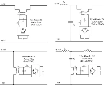
2.3.2Circuit Topologies
In a DCAPF, an active modulator acts on the DC-bus such that it can controllably decouple any unwanted ripples and/or disturbances on the DC-bus. The modulator can be put in series acting as a controllable voltage source, or in parallel acting as a controllable current source. The operational concept is shown in Figure 10 in which the series modulator is acting as “Series DC Active Filter” (SDAF), and the parallel modulator is acting as a “Parallel DC Active Filter” (PDAF). The combination of these DCAPFs with passive filter leads to different hybrid topologies that are shown in Figure 11. A hybrid topology might be preferred over a pure active filtering solution due to better performance and size reduction of active elements in the modulator. On the other hand, the solution must be optimized such that it will not increase the cost or total size of the integrated system of rectifier and filter.
impedance of DCAPF is not large enough compared to the impedance of load, i.e. at high load conditions, the ripple rejection and filtering performance of PDAF deteriorates for a given active filter rating [35], [37]. In series configuration though this is not the case. When the DCAPF is put in series with load, it shares the ripple voltage with load. Thus, it can be controlled such that the ratio of the injected ripple impedance by SDAF is far greater than load impedance; then practically independent of the load impedance, very small ripple voltage is produced across load terminals [35]. A relative comparison of active filter compensation performance is presented in Figure 12. As it can be seen, SDAF performance, especially at controller gain of unity, is superior to PDAF independent of load, whereas PDAF performance degrades with decreasing load. Therefore, SDAFs have better filtering performance over the parallel configuration due to its injected impedance being independently controllable regardless of load impedance at ripple harmonic frequencies.
2.4
Series DC Active Filter (SDAF) in MVDC System
For the MVDC system integrated with series DC active power filter (SDAF), both “phase-controlled rectifier” (PCR) and “active front-end” (AFE) rectifiers are considered. In both cases a hybrid series dc active filtering solution is adopted. The reason as will be demonstrated is that a hybrid filtering solution reduces active filter rating and results in better filtering performance.
2.4.1 Active Front-End (AFE)-based MVDC System
I. Proposed Series DC Active Filter Control Scheme
The controller structure and its associated control block diagrams for the SDAF is provided in [11] and is shown in Figure 14. It consists of three major control loops in order to perform the desired functions. The final goal is to produce a voltage ripple at the output terminals – secondary or DC-side - of SAI’s coupling transformer which is as close as possible, in all its signal attributes, to ripple components present at the output of the AFE rectifier but which possess an opposite phase in order to cancel each other out. Achieving this goal, the final DC-bus voltage post SAI will be smooth and free of the disturbances that would otherwise be there due to FE rectifier and active load non-linear interactions. SDAF consists of an H-bridge inverter, output switching ripple filter, and an output transformer which couples it to the MVDC-bus. It is the reference voltage to the PWM modulator of inverter which demands SDAF to produce a specific ripple component at its output. Due to hardware implementation limitations such as limited switching frequency, limited bandwidth, improper switching events, dead-time effect, and so on, not all and every single harmonic component is reproduced as it was intended to. It is the function of the control system to consider all those practical hardware limitations and non-idealities and, in closed-loop feedback control fashion, generate a reference voltage signal to the PWM modulator such that series active injection is made certain up to a specific frequency.
Figure 14 Series active injector – SDAF - controller block diagram [11].
a) DC Error Elimination b) Harmonic Extraction c) Band-Pass Damping
During transient loading conditions, SDAF’s output transformer can support a transitory DC voltage component which can lead to both DC saturation and error at the output terminals of the MVDC system. DC saturation can force SDAF to shut down; and thus, leave the system prone to disturbances. DC error is never good since it might disrupt the operation of loads that are hanging from DC-bus. As it is shown in block (a) in Figure 14, the injected output voltage ripple is measured and low-pass filtered (LPF) with a cut-off frequency of 1 Hz in order to extract the DC component; then, it is compared against a zero reference
AC/DC rectifier
Rs
Vs Vin
Series Active Injector (SAI) LPF1
V*dcref = 0
PI Harmonic Extraction DC Error Elimination LPF1 Gain K PWM Modulator LPF1 A c ti v e L o a d iload vo Active load DC supply n :1 Vripple_inj PI V* ref-int
voltage and the error is fed to a PI controller to make sure it is regulated to zero. The cut-off frequency of LPF1-(a) in Figure 14 is set to 1 Hz.
Block (b) in Figure 14 shows the “harmonic extraction unit” in SDAF’s controller structure. This block is considered the most important block in the controller structure since it is responsible for extracting the ripple component out of AFE rectifier’s output voltage and for conditioning it for active filter inverter. This provides SDAF/SAI with the ability to compensate for any oscillations resulting from the non-linear interaction of active loads hanging from the DC-bus and the main AFE rectifier. This is very important since the amplitude of such oscillations might get high enough at high powers to disturb all the other loads hanging from the same bus. The first control loop in harmonic extraction unit with LPF1-(b) cut-off frequency set to 1 Hz, extracts the whole ripple; and then, LPF2-(b) limits it to 1 kHz which is 1/20th of active filter inverter’s 20 kHz switching frequency. The inverter effective bandwidth is 2.2 kHz which is actually 1/9th of the switching frequency. LPF2-(b) cut-off frequency is chosen to be half the bandwidth such that it is made sure that the inverter is able to exactly reproduce those ripple components. This is due to the fact that even within converter bandwidth, because of dead-time effect, probable improper switching events, and other uncertainties, the inverter might not be able to perfectly reproduce its commanded reference voltage.
responsible for performing that function. After extracting the ripple component from measured output voltage of SDAF through setting LPF1-(c) cut-off to 1 Hz, LPF2-(c) with a cut-off frequency of 2 kHz limits it to the bandwidth of active filter inverter. Frequency components up to 1 kHz are taken out by subtracting 𝑉𝑟𝑒𝑓−𝑖𝑛𝑣∗ from extracted measured ripple, and the remaining band-pass signal is forced to zero through a PI controller as it can be seen in Figure 14.
Figure 15 shows different functions of SDAF in the frequency domain. For frequencies up to 1 kHz, SDAF is performing active filtering to cancel the ripples out. For band-pass frequencies between 1 kHz and 2.2 kHz bandwidth of inverter, SDAF is actively damping the ripple frequencies. Finally, frequencies which are above bandwidth of inverter are passively filtered and damped by the special, 4th-order inverter output switching ripple filter which is elaborated in section for series active filter design.
Figure 15 Frequency domain representation of different functions of SDAF [11].
Figure 16 Steady-state performance of SDAF controller [11].
f0=1kHz Frequency
Voltage
f1=2.2kHz fsw=20kHz
SAI Active Filtering SAI Active Damping
Passive Filtering and Damping
4.2 4.25 4.3 4.35 4.4
-500 0 500
Steady-state performance of the SAI controller
Vri p p le ( v)
4.2 4.25 4.3 4.35 4.4
-500 0 500 VS A I-in j (v)
4.2 4.25 4.3 4.35 4.4
Figure 17 Transient performance of SDAF controller [11].
II. Series DC Active Filter Design
Figure 13 show the SDAF/SAI integrated into the MVDC system. The series active filter design is derived by the worst case voltage ripple and/or disturbance that it should follow. Since SADF is in series with the DC-link any ripple current forcibly passes through the SDAF after being transferred to primary side (AC-side) of the series coupling transformer. It is the slew-rate of this current that determines the critical output inductor of SDAF inverter. Knowing the current slew-rate, the DC-bus voltage value of inverter, and the switching frequency, the value of the inductor is chosen. A series of simulations are carried and the worst-case slew-rate is found to be 3 A/µs. Therefore, the value of the output inductor is chosen to be 200 µH. The DC-bus voltage of the inverter and the turns-ratio of the
4.95 5 5.05
-2000 0 2000
Transient performance of the SAI controller
V ri p p le ( v)
4.95 5 5.05
-2000 0 2000 V S A I-in j (v)
4.95 5 5.05
-2000 0 2000 Time (s) V m u x ( v) Vripple VSAI-inj
VMultiplexed VSAI-inj
Figure 18 SDAF output filter magnitude and phase frequency response [11].
Table 1 SDAF parameters
Inverter
Rated power (kVA) 20
DC-bus (V) 650
Switching Freq (kHz) 20
Transformer
Turns ratio (N2/N1) 4.5
Primary leakage inductance (uH) 0.3
Secondary leakage inductance
(uH) 10
Output filter
Lf (uH) 200
Cf (uF) 10
LT (uH) 128
CT (nF) 500
Rd (ohm) 4
-40 -30 -20 -10 0 10 M a g n itu d e ( d B )
100 101 102 103 104 105
-180 -135 -90 -45 0 P h a s e ( d e g ) Bode Diagram
III. AFE-based MVDC System Simulation Results with SDAF
In Figure 20, the 500-kW load step-down transient condition of MVDC system is zoomed out with and without SDAF in operation. As it can be seen from Figure 20a, the MVDC-bus undergoes a 1.7 kV (~ 22%) voltage overshoot without SDAF, whereas the overshoot is reduced to only 150 V (2%) with SDAF operation in Figure 20b.
In Figure 21, the 500-kW load step-up transient condition of MVDC system is zoomed out with and without SDAF in operation. As it can be seen from Figure 21a, the MVDC-bus undergoes a 2.2 kV (~ 29%) voltage overshoot without SDAF, whereas the undershoot is reduced to only 240 V (3.2%) with SDAF in operation. Also, it can be observed that the steady-state ripple amplitude is reduced to less than 50 V peak-to-peak as compared to the 500 V when SDAF is not in operation. Actually, the active damping function of SDAF is taking care of the transient conditions while the active filtering function is filtering out any steady-state oscillations induced on the DC-link.
Figure 20 MVDC bus voltage response to 500-kW step-down load change without SDAF in operation (a) and with SDAF in operation (b) [11].
2.4.2 Phase-Controller Rectifier (PCR)-based MVDC System I. The Proposed Circuit Topology
The proposed MVDC power supply system main circuit is shown in Figure 22 [39]. It consists of four parts: 12-pulse front-end rectifier, passive low-pass LCR filter, transformer-coupled series DC active power filter, and loads. In Figure 22, the 12-pulse thryistor-bridge comprises two 6-pulse PCRs connected in parallel at AC-side and in series at output DC-side. The passive low-pass filter, immediately after thyristor-bridge, partially filters out high frequency ripples well beyond SDAF bandwidth. Then, SDAF can remove nearly all of the undesired ripples left after passive filtering. As it can be seen in the power circuit diagram, SDAF deploys a special fourth-order output filter to eliminate switching frequency ripple and damp out unwanted harmonic frequencies between active filter effective bandwidth and the switching frequency. The primary side (AC-side) of the series dc coupling transformer is connected to active filter output filter and the secondary side (DC-side) is connected in series with the MVDC-bus. The SDAF has the same parameters as given in Table 1.
II. Series DC Coupling Transformer (SDCT)
ripple when magnetizing current is held constant. A more thorough investigation of SDCT parameters impact of SDAF rating follows in the section 2.4.3.
Figure 23 AC magnetizing current vs. DC voltage ripple.
Figure 24 SDAF kVA rating versus DC voltage ripple. 0.3 0.57 0.79 0.98 1.15 0 0.2 0.4 0.6 0.8 1 1.2 1.4
0 10 20 30 40 50
V d c ri p p le (kV p ea k-to -p ea k)
Magnetizing Current (%) APF Size = 50 kVA
1.15
1.02 0.95
0.88 0.82
0 0.2 0.4 0.6 0.8 1 1.2 1.4
0 200 400 600 800 1000
V d c ri p p le (kV p e ak -to p e ak)
III. PCR-based MVDC Simulation Results with SDAF
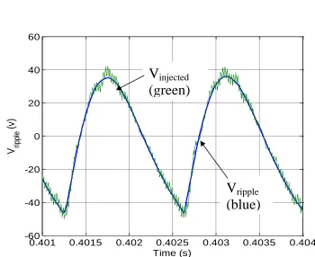
The steady-state simulation results of PCR-based MVDC system integrated with SDAF are presented here. The goal is to verify the operation and filtering performance of SDAF assuming the SDCT not to suffer from any DC bias/saturation problem. A system similar to the circuit shown in Figure 22 is designed and simulated in MATLAB/Simulink. The system parameters are given in Table 2. Figure 25 shows the MVDC-bus voltage before and after SDAF operation and Figure 26 shows load current AC ripple component. DC-bus voltage AC ripple harmonic profile analysis is provided in Table 3. As it can be seen, a total AC ripple compensation of 91% is achieved while the 12th harmonic component is compensated more than 98%.Figure 27shows magnified AC ripple voltage after output of passive filter of PCR together with the injected AC voltage from SDAF. As is can be seen, SDAF injected voltage across DC-bus is almost perfectly tracking the ripple voltage. On the other hand, this means that the injected impedance ratio is really high or k (SDAF controller gain) is very close to one. That is shown in Figure 28.
Table 2 Simulated PCR-based MVDC system parameters
3ph AC voltage Vs-ln kVrms 5.25
12-pulse thyristor bridge
DC reference Vdc kV 7.5
Output passive filter
Lp mH 15
Cr uF 3.44
Rp mΩ 66
DC Active Power Filter
N2/N1 - 4.5
DC bus V 450
Table 2 Continued
DC load (resistive) PL MW 3.75
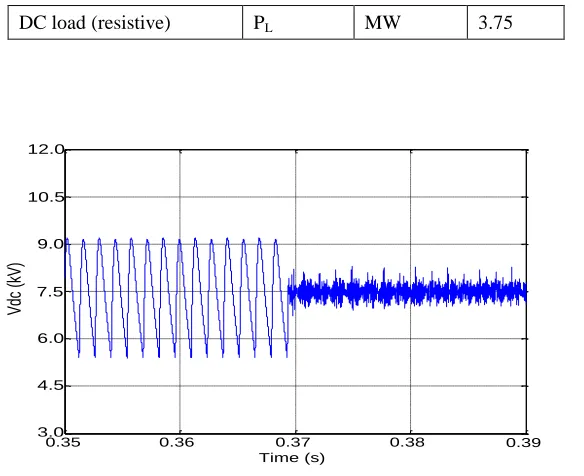
Figure 25 MVDC-bus voltage AC ripple before and after SDAF operation [39].
Figure 26 DC load current AC ripple component before and after SDAF operation [39].
0.35 0.36 0.37 0.38 0.39
40 60 80 100 120 140 160 Time (s) V dc (V ) 7.5 9.0 10.5 12.0 6.0 4.5 3.0 V dc (k V )
0.35 0.36 0.37 0.38 0.39
Time (s)
0.35 0.36 0.37 0.38 0.39
-0.25 -0.2 -0.15 -0.1 -0.05 0 0.05 0.1 0.15 0.2 0.25 Time (s)
I rippl
Table 3 MVDC voltage ripple harmonic profile w/o and w/ SDAF
APF
Load ripple voltage harmonics spectrum
(kV) RF
(%) CMPF DC
(kV) 12
th
24th 36th 48th 60th
w/o
7.5 1.59 0.51 0.21 0.12 0.07 16 - w/ 0.03 0.04 0.01 0.05 0.04 2.4 91
Figure 27 AC voltage ripple after passive filter in PCR-based MVDC system and injected AC ripple by SDAF [39].
0.401 0.4015 0.402 0.4025 0.403 0.4035 0.404
-60 -40 -20 0 20 40 60
Time (s)
V rip
pl
e
(
v)
V
injected(green)
V
rippleFigure 28 SDAF injected impedance ratio with respect to load impedance at different characteristic harmonic frequencies [39].
2.4.3 Factors Influencing Active Filter Sizing
The study here mainly focuses on some of the important parameters affecting the rating and performance of active filter. These parameters can be internal with respect to series active filter system, i.e. inverter parameters, coupling transformer etc., or external, as in line transformer leakage reactance to front-end rectifier. The parametric search will done in steady-state mode. The goal is to understand how those set of parameters affect SDAF rating.
I. Series Coupling Transformer
internal parameters is shown in Figure 29. The transformer has three main parameters: 1) magnetizing inductance (Lm); 2) winding resistances and reactances (R1, L1, R2, L2); and 3) winding turns ratio (N2/N1).
Figure 29 Transformer model considered for steady-state SDAF rating study.
SDAF parameters are as given in Table 1. The transformer parameters are per-unitized according to the following base values:
Sbase-trans = Sbase = 7.5MVA Vb-pri = 650 V
Vb-sec = 2925 V
2.4.3.I.2 Effect of Magnetizing Inductance (Lm)
To study the impact of the magnetizing inductance on the rating and performance, the following transformer parameters are assumed to be constant:
N2/N1 = 4.5
R1 (2%) = 0.00112 Ω L1 (2%) = 3 uH R2(2%) = 0.0228 Ω L2(2%) = 60.4 uH
Comparative analysis of impact of different magnetizing inductance values on the series dc active filter rating and performance are presented in Table 4 and Table 5. It can be observed that higher values of inductance reduce the rating of the active filter. In addition, compensation factor (CMPF) and ripple factor (RF) improves with higher inductance as shown. We define these performance factors as (2-1) and (2-2). The results of the analysis are demonstrated in Figure 30 and Figure 31.
𝐶𝑀𝑃𝐹 (%) =𝑉̃𝑑𝑐−𝑡ℎ𝑦− 𝑉̃𝑑𝑐−𝑙𝑖𝑛𝑘
𝑉̃𝑑𝑐−𝑡ℎ𝑦 ∗ 100
(2-1)
𝑅𝐹 (%) =𝑉̃𝑑𝑐−𝑙𝑖𝑛𝑘
𝑉𝑑𝑐−𝑙𝑖𝑛𝑘∗ 100
Table 4 Effect of magnetizing inductance on active filter rating and performance for Lm = 0.3 pu, 100% rated load (a), and 10% rated load (b).
Lm (p.u.) LOAD (% rated) APF rating (kVA)
Vripple-pk Vapf-sec-pk CMPF
(%) RF (%) + – + – 0.3 (45uH)
10 65 2300 2300 500 500 18 20.5
100 17 430 1270 400 560 29.5 5.5
(a) (b)
Table 5 Effect of magnetizing inductance on active filter rating and performance for Lm = 30 pu, 100% rated load (a), and 10% rated load (b).
Lm (p.u.) LOAD (% rated) APF rating (kVA)
Vripple-pk Vapf-sec-pk CMPF
(%) RF (%) + – + – 30 (4500 uH)
10 25 3150 2750 2950 2650 94 2.1
100 25 2860 2900 2900 2800 98 0.6
(a) (b)
0.104 0.1045 0.105 0.1055 0.106 0.1065 0.107 -3000 -2000 -1000 0 1000 2000 3000 Time (s) V ri p p le ( v )
0.401 0.4015 0.402 0.4025 0.403 0.4035 0.404 -3000 -2000 -1000 0 1000 2000 3000 Time (s) V ri p p le ( v )
0.104 0.1045 0.105 0.1055 0.106 0.1065 0.107 -3000 -2000 -1000 0 1000 2000 3000 Time (s) V ri p p le ( v )
Figure 30 Series dc active filter rating vs. magnetizing inductance for 10% and 100% rated load current.
2.4.3.I.4 Effect of Winding Resistance and Leakage Inductances (R1, L1, R2, L2)
In this study the magnetizing inductance and turns ratio are assumed to be constant at Lm = 1 p.u. (150 uH) and N2/N1 = 4.5. The effect of leakage resistance and inductance is presented in Table 6. It can be observed that although the active power filter rating has increased, the filtering performance does not change very much.
Table 6 Effect of leakage resistance and inductance on series dc active filter rating
Lm (p.u.) LOAD
(% rated)
APF rating (kVA)
R&L (%)
CMPF (%) RF
(%)
1 (150 uH)
10 110 2 42.5 15.5
40 38.5 16.3
100 44 2 64.4 4.5
40 73.3 4
2.4.3.I.5 Effect of Turns Ratio (N2/N1)
Table 7 Effect of transformer turns ratio on active filter rating and performance for N2/N1 = 4.5, 100% rated load (a), and 10% rated load (b).
N2/ N1 LOAD (% rated) APF rating (kVA)
CMPF (%) RF
(%)
4.5
10 110 42.5 15.5
100 44 64.4 4.5
(a) (b)
Table 8 Effect of transformer turns ratio on active filter rating and performance for N2/N1 = 10, 100% rated load (a), and 10% rated load (b).
N2/ N1
LOAD (% rated)
APF rating (kVA) CMPF (%) RF
(%)
10
10 114 93.4 2.2
100 114 98.7 0.4
(a) (b)
0.104 0.1045 0.105 0.1055 0.106 0.1065 0.107 -3000 -2000 -1000 0 1000 2000 3000 Time (s) V ri p p le ( v )
0.401 0.4015 0.402 0.4025 0.403 0.4035 0.404 -3000 -2000 -1000 0 1000 2000 3000 Time (s) V ri p p le ( v )
0.104 0.1045 0.105 0.1055 0.106 0.1065 0.107 -3000 -2000 -1000 0 1000 2000 3000 Time (s) V ri p p le ( v )
Figure 32 Series dc active filter rating versus turns ratio.
II. Input Line Transformer Leakage Reactance (Xs)
This parametric search is carried out over a 7.5 MVA, 5 kV MVDC system with regard to input line transformer reactance in order to determine the rating of SDAF under worst-case firing angle and different resistive loading conditions. As it is known, the DC-side AC ripple of a thyristor-bridge rectifier is an increasing function of firing angle. For regular system operation, the angle is in the range of 15-25 degrees, not having very drastic DC-side ripple and not demanding very large input reactive power. Moreover, the normal operating angle is chosen as such in order to accommodate for both AC line voltage sags and swells. Since voltage swell disturbance increase the DC-side ripple and demands for more compensation effort by SDAF, a worst-case input phase voltage swell of 30% is considered over the period of simulation. That disturbance requires a firing angle of 45˚ in order to keep the DC output voltage constant at 5 kV. Having a firing angle of 45˚, two extreme cases for the input, AC-side reactance are conAC-sidered: 1% and 10% of base value. The point here is that the AC-AC-side reactance value changes the slew-rate of AC ripple voltage on the DC-side. The larger the input reactance, the smaller the voltage ripple slew-rate; thus, the smaller the current ripple slew-rate becomes. The smaller the slew-rate, the better the SDAF inverter is able to compensate for the thyristor-bridge output voltage ripple. The system schematic is similar to Figure 22 except that the front-end is a 6-pulse thyristor-bridge. The SDAF parameters are:
Transformer turns ratio (N2/N1) = 6 DC-link voltage = 700 V
![Figure 6 An integrated naval ship MVDC power system with different kinds of load hanging from DC-bus [1]](https://thumb-us.123doks.com/thumbv2/123dok_us/1568380.1192799/37.612.142.489.71.325/figure-integrated-naval-mvdc-power-different-kinds-hanging.webp)
![Figure 9 MVDC-bus voltage dynamics under 500-kW step load changes (a), zoomed out voltage response for the load step-down (b), and zoomed out voltage response for the load step-up (c) [11]](https://thumb-us.123doks.com/thumbv2/123dok_us/1568380.1192799/41.612.110.518.148.355/figure-voltage-dynamics-changes-voltage-response-voltage-response.webp)
![Figure 14 Series active injector – SDAF - controller block diagram [11].](https://thumb-us.123doks.com/thumbv2/123dok_us/1568380.1192799/48.612.122.509.66.288/figure-series-active-injector-sdaf-controller-block-diagram.webp)
![Figure 15 Frequency domain representation of different functions of SDAF [11].](https://thumb-us.123doks.com/thumbv2/123dok_us/1568380.1192799/51.612.156.453.372.610/figure-frequency-domain-representation-different-functions-sdaf.webp)
![Figure 17 Transient performance of SDAF controller [11].](https://thumb-us.123doks.com/thumbv2/123dok_us/1568380.1192799/52.612.156.473.84.319/figure-transient-performance-sdaf-controller.webp)
![Figure 18 SDAF output filter magnitude and phase frequency response [11].](https://thumb-us.123doks.com/thumbv2/123dok_us/1568380.1192799/54.612.152.476.400.625/figure-sdaf-output-filter-magnitude-phase-frequency-response.webp)