Abstract
SCHOENFLIESS, KORY MICHAEL. Performance Analysis of System-on-Chip Applications of Three-dimensional Integrated Circuits (Advisor: Dr. W. Rhett Davis)
In the research community, three-dimensional integrated circuit (3DIC) technology
has garnered attention for its potential use as a solution to the scaling gap between MOSFET
device characteristics and interconnects. The purpose of this work is to examine the
performance advantages offered by 3DICs. A 3D microprocessor-based test case has been
designed using an automated 3DIC design flow developed by the researchers of North
Carolina State University. The test case is based on an open architecture that is exemplary of
future complex System-on-Chip (SoC) designs. Specialized partitioning and floorplanning
procedures were integrated into the design flow to realize the performance gains of vertical
interconnect structures called 3D vias. For the post-design characterization of the 3DIC,
temperature dependent models that describe circuit performance over temperature variations
were developed. Together with a thermal model of the 3DIC, the performance scaling with
temperature was used to predict the degree of degradation of the delay and power dissipation
of the 3D test case. Using realistic microprocessor workloads, it was shown that the
temperatures of the 3DIC thermal model are convergent upon a final value. The increase in
delay and power dissipation from the thermal analysis was found to be negligibly small when
compared to the performance improvements of the 3DIC. Timing analysis of the 3D design
and its 2D version revealed a critical path delay reduction of 26.59% when opting for a 3D
implementation. In addition, the 3D design offered power dissipation savings of an average
PERFORMANCE ANALYSIS OF SYSTEM-ON-CHIP APPLICATIONS OF
THREE-DIMENSIONAL INTEGRATED CIRCUITS
by
KORY MICHAEL SCHOENFLIESS
A thesis submitted to the Graduate Faculty of North Carolina State University
in partial fulfillment of the requirements for the degree of
Master of Science
In
COMPUTER ENGINEERING
Raleigh, NC
2005
Approved by:
______________________________ ______________________________
Dr. Paul Franzon Dr. Douglas Barlage
______________________________
Dr. W. Rhett Davis
To my loving grandparents, Frank and Helen King, who sadly passed away during my time
Biography
Kory Michael Schoenfliess was born on August 25, 1981 in Rosedale, a suburb of
Baltimore, Maryland. Kory has spent most of his life in Maryland, and only recently moved
away from the State to pursue graduate studies. He is the son of Lothar and Sharon
Schoenfliess, who both still reside in Rosedale. Kory’s interest in computer technology was
spurred by his attendance of Eastern Technical High School of Essex, Maryland, where he
concentrated in engineering. In 1999, Kory was accepted to the University of Maryland,
Baltimore County and given an academic scholarship for his exemplary achievement in High
School. Shortly before leaving UMBC, Kory was blessed to meet his fiancé, Valerie Beach.
Kory graduated Summa Cum Laude in December 2003. By January of the next year, Kory
was attending North Carolina State University in pursuance of his Masters in Computer
Engineering.
Kory’s work experience includes a research internship at the University of Maryland,
College Park where he mostly functioned as a test engineer for fabricated ASICs in the ECE
department. The summers and winters of 2004 and 2005 were spent at the Columbia,
Maryland business unit of Scientific Applications International Corporation (SAIC), where
he was the hardware engineer on a project involving the design and testing of FPGA
Acknowledgements
First and foremost, I would like to thank my parents for giving me the opportunity
and support to succeed in higher education institutions. They are responsible for keeping me
grounded in life’s most important values. At every critical milestone in my life, my parents
have been there for direction and kind words.
I would also like to acknowledge the loving support of my fiancé, whose strength and
hopefulness during my time in North Carolina was remarkable. Without her dedication, I
never could have ventured as far as I did.
A great deal of credit should be given to my advisor, Dr. W. Rhett Davis. Dr. Davis
initially brought me to NC State and has seen me through my entire Masters degree. He
never was at a loss for ideas to surmount any problems I had with in my research, and his
enthusiasm in doing so is commendable. I would also like to thank Dr. Paul Franzon and Dr.
Doug Barlage for serving so graciously on my Advisory Committee.
My “colleagues” in graduate school also deserve notice for their help in classes,
research, and maintaining my sanity during the busiest times of each semester. In no
particular order, I would like to thank the following people: Chris Mineo, Samson Melamed,
Table of Contents
List of Tables ... vii
List of Figures ... viii
1 Introduction... 1
2 Temperature Dependent Models for use in 3DICs ... 5
2.1 Power Dissipation Temperature Dependence ... 5
2.1.1 Model Derivation ... 6
2.1.2 Model Verification... 9
2.2 Delay Temperature Dependence... 12
2.2.1 Model Derivation ... 12
2.2.2 Model Verification... 14
3 Testcase Power Dissipation and Delay Estimation Flow ... 17
3.1 Initial Power Dissipation Estimation Flow ... 17
3.1.1 Forward Annotation SAIF File ... 19
3.1.2 Synopsys PLI 3.0 ... 20
3.1.3 RTL Simulations with NC-Verilog... 21
3.1.4 Back Annotation of Switching Activity in Power Compiler ... 23
3.1.5 Back Annotation of Parasitics in Power Compiler ... 24
3.1.6 Report Power in Power Compiler ... 24
3.2 Initial Delay Estimation Flow... 25
3.3 Converging to Final Power Dissipation and Delay Values ... 26
3.3.1 Thermal Model of a 3DIC... 27
3.3.2 Temperature-Power Positive Feedback Loop ... 29
4 The FDSOI 3D Process... 33
4.1 3D Circuit Fabrication ... 33
4.2 Changes to the 2D Design Environment... 35
5 The ORPSOC Architecture... 39
5.1 Architecture Selection and Modification ... 39
5.2 OpenRISC 1200 Microprocessor (OR1200)... 41
5.2.1 Central Processing Unit (CPU)... 42
5.2.2 Instruction and Data Caches ... 45
5.2.3 Instruction and Data Memory Management Units (MMUs) ... 45
5.2.4 OpenRISC Wishbone Interfaces ... 46
5.3 Wishbone Traffic Cop... 46
5.4 Instruction and Data Memory Controller... 47
5.5 Instruction and Data SRAMs ... 47
6 Testcase Physical Design ... 50
6.1 Design Compiler Synthesis... 52
6.2 Manual User Tier Partitioning ... 53
6.3 3D Via Insertion according to User Partitioning ... 59
6.4 Initial SoC Encounter Floorplanning and Placement... 62
7 Results... 83
7.1 2D and 3D Path Delay Comparison... 84
7.2 2D and 3D Power Dissipation Comparison ... 85
7.3 Temperature Convergence and Performance Degradation Analysis ... 87
8 Conclusion ... 96
List of Tables
Table 2-1: Leakage power model as compared to SPICE simulations ... 11
Table 7-1: Path delay data from the 2D and 3D designs ... 85
Table 7-2: Power dissipation data for the single most active program profile ... 86
Table 7-3: Power dissipation data for the merged switching activity profile ... 87
Table 7-4: Power dissipation data for the worst case switching activity profile ... 87
Table 7-5: Assumptions for the 3DIC thermal model ... 88
List of Figures
Figure 1-1: ITRS Data for the Total Interconnect Length of an IC ... 1
Figure 1-2: ITRS Data for Interconnect RC Delay for three types of interconnect... 2
Figure 2-1: Normalized average short circuit energy for a CMOS inverter ... 7
Figure 2-2: Predicted versus actual leakage lower for an inverter... 10
Figure 2-3: Predicted versus actual leakage Power for a full adder ... 11
Figure 2-4: Predicted versus actual leakage power for a 16-bit ripple carry adder ... 11
Figure 2-5: Predicted versus actual delay of an FO-4 inverter ... 15
Figure 2-6: Predicted versus actual delay of an AND gate... 15
Figure 2-7: Predicted versus actual delay of a 16-bit ripple carry adder ... 16
Figure 3-1: Flow for obtaining the power dissipation of the ORPSOC test case ... 18
Figure 3-2: Format of the forward annotation SAIF file ... 19
Figure 3-3: Synopsys PLI 3.0 functions in the test bench [15]... 21
Figure 3-4: Format of the backward annotation SAIF file ... 23
Figure 3-5: Flow for obtaining timing delay values of the ORPSOC test case ... 25
Figure 3-6: Simplified thermal model of a 3DIC... 29
Figure 3-7: Temperature-power positive feedback loop... 32
Figure 4-1: Generalized breakdown of a 3D fabrication process ... 33
Figure 4-2: Example 3D circuit at the end of the FDSOI 3D process [20] ... 35
Figure 4-3: Tier A of the inverter chain... 36
Figure 4-4: Tier B of the inverter chain ... 36
Figure 4-5: Tier C of the inverter chain ... 36
Figure 4-6: Inverter chain layout showing all tiers ... 37
Figure 5-1: High level block diagram of the ORPSOC test case [2] ... 41
Figure 5-2: High level block diagram of the CPU [2] ... 43
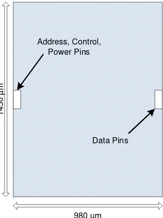
Figure 5-3: High level view of the SRAM layout... 49
Figure 5-4: Graphical representation of the SRAM LEF file ... 49
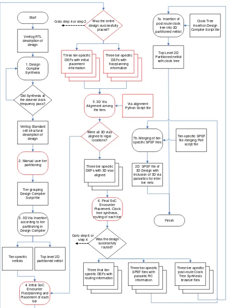
Figure 6-1: The logical progression through the 3DIC design flow... 51
Figure 6-2: Example 2D rectilinear net length interconnecting five blocks ... 54
Figure 6-3: Example 3D net length interconnecting five blocks ... 55
Figure 6-4: Partitioning scheme employed for the ORPSOC test case ... 58
Figure 6-5: Another partitioning strategy considered for the test case ... 59
Figure 6-6: 3D via insertion into the netlist ... 61
Figure 6-7: Example of good and bad floorplanning for 3DICs... 63
Figure 6-8: Procedure for initial placement of tier-specific netlists ... 65
Figure 6-9: Core size and module floorplanning for tier B of the ORPSOC test case ... 67
Figure 6-10: Core size and module floorplanning for tier A of the ORPSOC test case ... 69
Figure 6-11: Core size and module floorplanning for tier C of the ORPSOC test case ... 70
Figure 6-12: Initial placement result for tier B of the ORPSOC test case... 73
Figure 6-13: Initial placement result for tier A of the ORPSOC test case... 74
Figure 6-14: Initial placement result for tier C of the ORPSOC test case... 75
Figure 6-15: Center of core area for tier A and tier B after 3D via alignment ... 78
Figure 6-16: Routed tiers of the ORPSOC test case ... 80
Figure 7-1: The 2D ORPSOC test case after detailed routing ... 84
Figure 7-3: Thermal model temperatures for the merged switching activity profile... 90
Figure 7-4: Thermal model temperatures for the worst case switching activity profile ... 90
Figure 7-5: Change in total leakage power from ambient temperature ... 92
Figure 7-6: Percentage of tier delay increase from ambient temperature ... 93
1 Introduction
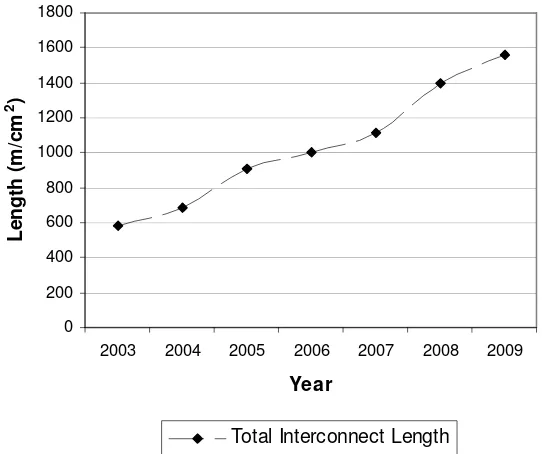
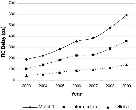
The International Technology Roadmap for Semiconductors (ITRS) predicts the rapid
increase in total interconnect length in the coming technology generations. In just three years,
the amount of active wiring that will be necessary for traditional integrated circuits is
expected to nearly double. Compounding the design challenges of engineers even more is the
outlook for interconnect RC delays. In the same timeframe, the delays for local, intermediate,
and global wiring are expected to increase by no less than 25% [1]. These trends can be seen
in Figure 1-1 and Figure 1-2.
0 200 400 600 800 1000 1200 1400 1600 1800
2003 2004 2005 2006 2007 2008 2009
Year
L
e
n
g
th
(
m
/c
m
2 )
Total Interconnect Length
0 100 200 300 400 500 600 700
2003 2004 2005 2006 2007 2008 2009
Year
R
C
D
e
la
y
(
p
s
)
Metal 1 Intermediate Global
Figure 1-2: ITRS Data for Interconnect RC Delay for three types of interconnect
Although the nominal gate delays will continue to decrease with each successive
generation for quite some time, the same cannot be said about the performance of the
metallization used to provide connectivity between these gates. The apparent scaling gap
between MOSFET device and interconnect performance has caused researchers to gain an
interest in three-dimensional integration as a possible solution to the foreseeable limitations
of standard two-dimensional circuit design. Three-dimensional integrated circuits (3DICs)
alleviate the delay concerns of interconnects by offering the vertical axis as a possible routing
direction. With the increasing popularity of System-on-Chip (SoC) architectural solutions,
3DICs can meet the density and functionality demands of these complex systems by
“stacking” multiple tiers vertically and realizing inter-tier connectivity by means of short,
In this work, a realistic 3D design test case based on the OpenRISC microprocessor is
presented in order to qualify the relative advantages of 3DICs. Specifically, the design of an
IC based on the OpenRISC Reference Platform System-on-Chip (ORPSOC) is detailed [2].
The test case is created by means of the 3DIC design flow of the Methodologies for
User-Friendly System-on-a-chip Experimentation (MUSE) research group at North Carolina State
University. This design flow is specific to MIT Lincoln Lab’s fully-depleted
silicon-on-insulator (FDSOI) 3D process [3]. Moreover, the design flow is unique in that it takes full
advantage of the maturity of industry-standard 2D Electronic Design Automation (EDA)
tools and simply adapts them to the 3D environment. It will be shown that, through
intelligent user partitioning between the tiers and floor planning within each tier of a 3DIC, a
3D microprocessor-based design can operate at a higher clock frequency than feasible for a
two-dimensional IC. The consideration of the performance gains from porting the design to
3D will also include the complexity issues of integrating multiple fabricated tiers in one
package. These issues are largely a function of the thermal model of a 3DIC, which
introduces the well-known poor heat removal ability of a multi-tiered chip [4]. Skeptics have
always pointed to the concerns of the higher average chip temperatures of 3DICs, and this
work will do the same.
In general, the interplay between a circuit’s delay, power dissipation, and operating
temperature has a degrading effect on its performance. A chip that is operating at a higher
temperature will tend to slow down and dissipate even more power, which, in turn, will force
a positive feedback loop between the power dissipation and temperature of an IC [5]. This
work presents two models that can be used to predict the temperature dependence of power
degradation due to temperature in 3DICs. In doing so, this work presents an illustrative
example of the aforementioned temperature-power positive feedback loop using the
ORPSOC test case. It is shown that this iterative loop does converge upon a final average tier
temperature for the 3D ORPSOC design and that the temperature is not high enough to
counteract the speedup from using vertical interconnects.
The organization of this work is as follows. First, the derivation and verification of
the two temperature-dependent circuit parameter models is reported. Next, the tool flows for
estimating power dissipation and path delays of a 3D design are discussed. These will later
be used to assess the performance improvement when moving from 2D to 3D and include
consideration of heat generation in the 3DIC. Following the flow development, a brief
overview of the FDSOI 3D process is described. Subsequently, an outline of the ORPSOC
architecture used for the test case is presented. In particular, the discussion includes the
merits of the ORPSOC as a 3D case study and how the ORPSOC was modified for
experimentation. Afterwards, the 3DIC design flow used for the physical design of the test
case is detailed. Once it is understood how to can characterize a 3DIC for delay and power
per tier, the results from the timing and power analyses of the 2D and 3D designs can be used
to gauge the effectiveness of 3D integration for the test case. To conclude, a summary of this
work is presented in addition to ideas for areas of future work that could help reduce 3D
2 Temperature Dependent Models for use in 3DICs
The thermal performance of 3DICs is a hot topic in the research community and one that
still remains a mystery. A critical issue in the migration of interconnect-centric designs to the
3D environment is the non-uniform temperature profile across the tiers of a 3DIC. Since
every tier beyond the bottom-most is handicapped by having heat-sources (active transistors)
far away from the heat-removal fixtures, the average temperature of a tier increases as more
tiers are added to the 3D stack and hence, the reliability of the IC worsens. One can no longer
assume a single temperature from which to project the power and speed of an integrated
system once it is transitioned to 3D. Two temperature dependent models have been
developed and verified in this work to aid in the understanding of 3D circuit behavior. The
phenomena of temperature dependence on power dissipation and combinational path delay
are presented in this section. Acknowledging the temperature non-idealities, the former is
used in the estimation of the increase in power dissipation and the latter is utilized to
determine the degree to which a 3DIC slows down. Both of these models were verified
against the actual results given in SPICE simulations using BSIM SOI models [6]. Good
agreement is shown between these temperature dependent models and the complex transistor
model of BSIM.
2.1 Power Dissipation Temperature Dependence
Recently, power dissipation has emerged as a limiting factor on the performance of
integrated circuits. Circuit designers can no longer simply target speed as the ultimate
measure of a chip’s performance. The motivation for this is not only in the prevalence of
feature size of MOSFET devices. A great deal of interest in the power consumption of
traditional 2D ICs has brought about an onslaught of low-power design methodologies as
well as methods for the integration of power dissipation considerations into design flows.
Especially central to the design of 3DICs, any accurate consideration of power dissipation
must account for its dependence on the operating temperature of the dissipating device. With
each tier of a 3DIC operating at a different average temperature, the initial characterization of
power dissipation in the design flow could prove to be too optimistic.
2.1.1 Model Derivation
The three major sources of CMOS power dissipation are encapsulated in equation 2.1,
where Pdynamic is the contribution to total power dissipation from dynamic sources, Pdp is the
power dissipated from direct-path currents, and Pstatic is the portion of power dissipation that
is static [7].
static dp
dynamic
Total P P P
P = + + (2.1)
For the purpose of this work, direct-path power is ignored as it is generally a very
small ratio of the total dynamic power. Moreover, direct-path power is a function of the peak
current and node transition time. Both of these factors have opposite reactions to temperature
change. Indeed, peak current decreases with increases in temperature, while transition times
tend to increase (see section 2.2). The relative insensitivity of direct-path power to
temperature is shown in Figure 2-1. Figure 2-1 tracks the normalized average direct-path
energy of a CMOS inverter simulated with one rising and one falling transition, with the
9.50E-01 9.70E-01 9.90E-01 1.01E+00 1.03E+00 1.05E+00 2
5 32 39 46 53 06 67 74 81 88 95
1 0 2 1 0 9 1 1 6 1 2 3 Temperature (C) N o rm a li z e d E n e rg y
Average Short Circuit Energy
Figure 2-1: Normalized average short circuit energy for a CMOS inverter
When considering the final two components of power dissipation, it is well-known
that dynamic power is generally insensitive to temperature change [8], [9]. This is supported
by the accepted definition of dynamic power dissipation as shown in equation 2.2. In
equation 2.2, CL is the load capacitance of a gate, VDD is the supply voltage, f is the clock
frequency of the circuit, and α0->1 represents the probability that a clock event results in zero
to one transition at the output of a gate [7]. Since all of the variables presented in equation
2.2 are independent of temperature, this directly implies that dynamic power is also
independent of temperature. It is worth noting that the frequency of the clock is usually set
by a phase-locked loop (PLL), which is designed to be insensitive to temperature.
1 0 2
> − =C V f
α
Pdynamic L DD (2.2)
The equation for static power dissipation is shown in equation 2.3, where Ileak denotes
the sub-threshold leakage current that exists between the supply rails when a transistor is
inactive. It is this leakage current that gives static power dissipation its strong dependence on
DD leak static I V
P = (2.3)
As discussed in [10], leakage currents are becoming a significant problem in circuit
design as technology continues to scale. It is estimated by Berkeley predictive models in
future technologies that leakage power will become so high that it can no longer be taken
lightly [11]. Thus, when modeling temperature dependent parameters of a design, leakage
power dissipation must be considered. The BSIM 3.3 model for the MOSFET drain current
in the sub-threshold region is characterized in equation 2.4 and 2.5 [6].
t off th gs t ds nV V V V V V s
ds I e e
I
− − −
−
= (1 )
) (
0 (2.4)
2 0 0 ) 2 ( t s ch Si s V N q L W I
φ
ε
µ
= (2.5)
In these equations, Vt is the thermal voltage and is given by KBT/q, where T is the
temperature [6]. Although the BSIM model is complex, the scaling of drain current with
temperature can be approximately reduced to T2e1/T. Thus, leakage power is described as being exponentially dependent on temperature. In order to attempt to model this scaling
behavior from a reference operating temperature, two published leakage models were tested.
The first is from the work of [8] and is formulated directly from equations 2.4 and 2.5. This
temperature dependent leakage model is shown equation 2.6, where β represents a
curve-fitting parameter that is normally determined from SPICE simulation regressions.
T leak
leak T I T T e
I
β 2
0)*
( )
( = (2.6)
Equation 2.6 predicts the leakage current at any arbitrary temperature, Ileak(T), from a
time-SOI models. For this reason, a more-agreeable temperature dependent leakage model was
chosen. Shown in equation 2.7, this model was specifically tested against BSIM SOI models
and uses a second-order polynomial to describe the dependency [12]. The values for α1 and
α2 are found using curve-fitting techniques.
) 1
)( ( )
( T I T0 1 T 2 T2
Ileak ∆ = leak +α ∆ +α ∆ (2.7)
According to equation 2.7, leakage power at an arbitrary temperature can be predicted
using not the absolute temperature value but the departure from the reference temperature,
∆T. This model for leakage power more closely matched the actual values obtained from
SPICE simulations.
2.1.2 Model Verification
To determine the values for the curve-fitting parameters in equation 2.7, a series of
SPICE simulations were performed. Each test circuit was configured for a leakage power
measurement. The inputs to the circuits were giving a static bit pattern, and the current
through the supply was measured. The leakage power in watts is calculated by multiplying
the current through the supply with the nominal supply voltage, which was 1.5 volts for the
BSIM SOI model. The temperature parameter in SPICE was swept between 25 and 125
degrees Celsius, and the leakage power at each temperature was calculated. The test circuits
for simulation were a number of the MUSE SOI standard cells in addition to some larger
designs. Once all of the SPICE simulations were complete, the leakage power results from
SPICE were collected into files and taken as input to a small curve fitting C program. For
each test circuit, this program simply calculated the values of leakage power at every
temperature node, the percentage of error between the SPICE value and the value generated
from the model was saved. An average percentage of error was determined after all of the
temperature nodes were visited. This average represented the error between SPICE and the
model for one particular value of α1 and α2 . Iterations within a range of values for α1 and α2
were performed to arrive at the best possible error for each test circuit. The output of the
program was a file containing a set of values for α1 and α2 that gave the best possible error for
each test circuit. It was observed that the value for α1 was exactly the same for all test circuits
and that the value for α2 varied very little. This was consistent with the work of [12]. Figure
2-2, Figure 2-3, and Figure 2-4 together show the quality of the prediction capability of the
model versus the actual SPICE leakage power values. The test circuits for Figure 2-2, Figure
2-3, and Figure 2-4 are an inverter, a full adder, and a 16-bit ripple carry adder, respectively.
The figures show that inaccuracy in the model is only present near the upper limit set on
temperature. The model variables were set to 0.24 for α1 and 0.0005 for α2. Table 2-1
summarizes the leakage power error in the test circuits when using these values.
0.00E+00 5.00E-07 1.00E-06 1.50E-06 2.00E-06 2.50E-06 2 5 3 1 3 7 4 3 4 9 5 5 6 1 6 7 7 3 7 9 8 5
Tem perature (C)
L e a k a g e P o w e r (W ) Predicted Actual
Figure 2-3: Predicted versus actual leakage Power for a full adder
0.00E+00 5.00E-06 1.00E-05 1.50E-05 2.00E-05 2.50E-05 3.00E-05 3.50E-05 4.00E-05 4.50E-05 2 5 3 1 3 7 4 3 4 9 5 5 6 1 6 7 7 3 7 9 8 5
Tem perature (C)
L e a k a g e P o w e r (W ) Predicted Actual
Figure 2-4: Predicted versus actual leakage power for a 16-bit ripple carry adder
Table 2-1: Leakage power model as compared to SPICE simulations
Cell Name Average % of Error
INV 3.54
2-Input NOR 2.48
2-Input NAND 3.24
2-Input XOR 3.2
Full Adder 3.81
2.2 Delay Temperature Dependence
Techniques for estimating the frequency achievable for a design at a nominal operating
temperature are commonplace in the industry. Recently, interest has been invested in the
research of methods for calculating full-chip thermal profiles. Using this thermal profile, the
performance can be ascertained for specific temperatures at locations on the chip. The same
concept can be applied to the tiers of a 3DIC. Particularly, the temperature profile across the
tiers of a 3DIC can be used to estimate the slow down of the circuits on the each tier. This
slow down is measured by the increase in combinational path delay due to temperature
effects on MOSFETs. In a digital circuit, an increase in critical path delay has an inverse
effect on the maximum clock frequency attainable. Therefore, it is vital to gain an
understanding of the degree to which the speed of a 3D design derates from its synthesized
speed target. Modeling the temperature dependence of delay in a digital design from a
reference temperature is an efficient means of quickly estimating clock frequency
requirements.
2.2.1 Model Derivation
The MOSFET drain current, ID, can be expressed in terms of the alpha model shown
in equation 2.8 [13]. In this equation, µ(T) and VTH(T) denote the temperature dependence of
carrier mobility and threshold voltage, respectively.
α µ
α (T)(V V (T))
ID DD− TH (2.8)
while the other works in the opposite manner. It was noted in [13] that, for supply voltages
above one volt, the temperature dependence of carrier mobility tends to dominate. Hence, the
drive current of a MOSFET has an inverse dependence on temperature, and because of this,
the delay of a CMOS circuit will increase with temperature.
The model used to predict the temperature dependence of delay is largely based on
[14], which showed that any combinational delay will hold constant over a wide range of
technologies, temperatures, and voltages when normalized to the delay of an FO-4 inverter
that is subject to the same changes. It is for this reason that the FO-4 inverter delay is often
used as the metric for the speed of a technology. The term “FO-4” stands for “fan-out of
four” and implies a circuit composed of an inverter loaded by four copies of itself. As
opposed to measuring the delay increase with temperature for every circuit topology, one can
predict with relatively high accuracy the degree to which an arbitrary circuit will slow down
using the known slowdown of a FO-4 inverter at the same temperature. A prerequisite to
adopting this approach is the formulation of an equation to predict the slow down of the FO-4
inverter. The delay model that incorporates temperature scaling is shown in equation 2.9 [8].
) (
ξ
µ α
t dd
dd
V V
T V delay
− (2.9)
As in the case of the temperature dependent leakage model, µ and ξ are curve fitting
parameters. The logic in place here is that, once the behavior of an FO-4 inverter across a
temperature range is known, it is reasonable to assume that any combinational circuit will
behave similarly. Thus, consistency between equation 2.9 and SPICE simulations is required
2.2.2 Model Verification
The FO-4 inverter was designed using five identical copies of the smallest inverter in
the SOI standard library. To simulate this circuit in SPICE, the input was provided with a
signal having exactly one rising and one falling transition. The transition time was set to 100
picoseconds, and the delay for both transitions was calculated with measurement statements
in the netlist. The propagation delay was measured from the 50% points of the input and
output waveforms. The average of the two delays across a temperature range of 25 to 125
degrees Celcius was used to determine the values for the curve fitting parameters of equation
2.9. A similar procedure as detailed in section 2.1.2 was performed to find the best average
error between the model and the SPICE results. For the temperature range mentioned above,
the best error was found to be 0.88%, which corresponds to the values of 0.09 and 8.51 for µ
and ξ in equation 2.9, respectively. Figure 2-5 shows the predicted versus actual delay of the
FO-4 inverter. The y-axis of Figure 2-5 is the delay normalized to the reference temperature.
To verify that the FO-4 inverter is an excellent determinant for the temperature dependence
of delay, additional circuits were simulated. Figure 2-6 and Figure 2-7show the accuracy of
the model for an AND gate and a 16-bit ripple carry adder. The average error across the
0 0.2 0.4 0.6 0.8 1 1.2 1.4 2 5 3 2 4 0 4 8 5 6 6 4 7 2 8 0 8 8 9 6 1 0 4 1 1 2 1 2 0
Tem perature (C)
N o rm a li z e d D e la y Predicted Actual
Figure 2-5: Predicted versus actual delay of an FO-4 inverter
0.0 0.2 0.4 0.6 0.8 1.0 1.2 1.4 2 5 3 2 4 0 4 8 5 6 6 4 7 2 8 0 8 8 9 6 1 0 4 1 1 2 1 2 0 Tem perature N o rm a li z e d D e la y Actual Predicted 2
0.0 0.2 0.4 0.6 0.8 1.0 1.2 1.4 2 5 3 3 4 1 4 9 5 7 6 5 7 3 8 1 8 9 9 7 1 0 5 1 1 3 1 2 1
Tem perature (C)
N o rm a li z e d D e la y Actual Predicted
3 Testcase Power Dissipation and Delay Estimation Flow
Realistic power dissipation and timing delay values for the ORPSOC test case are
needed for evaluating the performance of a 3D design relative to a 2D one. Additionally, the
previous section’s formulation of temperature dependent models relies on accurate power
and delay numbers at a reference temperature as a starting point for any predictive
calculations. In this section, the procedure for characterizing the test case in terms of power
dissipation and combinational path delays is detailed. For an increased level of accuracy, the
parasitics of the wires in the layout of the test case (see sections 6.6 and 6.8) were
incorporated into this procedure. For the purposes of analyzing both the 3D and 2D designs
of the test case, the structure of the flows for obtaining power dissipation and delay values
are generalized.
3.1 Initial Power Dissipation Estimation Flow
The process of finding realistic power dissipation values for a complex design reduces
to realizing a switching activity profile that spans all of the nets in the design. Once the
switching activity is known, the appropriate tools can be used to analyze the design for power
dissipation. Recall from section 2.1.1 that switching activity of a gate is needed in the
calculation of dynamic power dissipation. The value for the leakage power of a gate is
constant (if using an average value) and is given in the standard cell library files once the
library is characterized for power. Creating the library files is beyond the scope of this work
and will not be covered here. It is assumed that every standard cell in the design has a
dissipation of the ORPSOC test case is shown in Figure 3-1. An explanation of each step
follows.
Create Forward Annotation SAIF
file in Design Compiler Verilog RTL description of design Forward Annotation SAIF file
Register nets for monitoring using Synopsys PLI 3.0
Binary Image of program to be loaded in test
bench Perform RTL
Simulation of original ORPSOC
in NC-Verilog
Backward Annotation SAIF
file
Load design and back-annotate switching activity
in Power
Compiler
Verilog structural description of design (post clock
tree synthesis)
Back-annotate wiring parasitics in
Power Compiler
Post-route SPEF file from SoC
Encounter
Report power in
Power Compiler
Finish Start
3.1.1 Forward Annotation SAIF File
A special type of file is used throughout this power flow to allow information
exchange between tools. Known as switching activity interchange format, or SAIF, this
Synopsys-developed file type streamlines the capturing and annotation of switching activity
for RTL and gate-level designs. To begin, a forward annotation SAIF file is created in
Design Compiler. Once written, this SAIF file contains a listing of all of the
“synthesis-invariant” components of the design with no appended switching activity information. The
classification of a port or net as being “synthesis-invariant” implies that it will be preserved
during the synthesis process. Objects that are “synthesis-invariant” include hierarchical ports
and sequential elements such as registers and memory arrays. The format of a forward
annotation SAIF file is shown in Figure 3-2. A similar format will be used later in the flow
for the back annotation SAIF file with the inclusion of switching activity information.
(SAIFILE
(SAIFVERSION "2.0") (DIRECTION "forward") (DESIGN )
(DATE "Mon Sep 12 23:15:04 2005") (VENDOR "Synopsys, Inc") (PROGRAM_NAME "rtl2saif") (VERSION "1.0")
(DIVIDER / ) (INSTANCE top (PORT (clk_i clk_i) (rst_i rst_i) …… ) ) File Header
Command in Design Compiler to generate file
Hierachical instance name Object type identifier
(PORT or NET)
Object List (abbreviated)
Figure 3-2: Format of the forward annotation SAIF file
To write a forward annotation SAIF file in Design Compiler, the RTL description of
interpret the design, compile a list of synthesis-invariant objects, and finally write a forward
annotation SAIF file. In an effort to exploit the existing RTL test bench that was packaged
with the ORPSOC, the SAIF file was written at the OR1200 level of hierarchy.
3.1.2 Synopsys PLI 3.0
Now that the forward annotation SAIF file has been created, it must be recognized by
a Verilog simulator before any switching activity can be captured. The mechanism to
integrate the information contained within the forward annotation SAIF file with the Verilog
simulator is the Synopsys PLI 3.0 [15]. “PLI” stands for programming language interface and
is a feature of the Verilog compiler that allows the linking and execution of standard C/C++
programs within a Verilog source file. PLI is most useful for calling programming language
functions within a test bench for statistical bookkeeping purposes. Synopsys provides Verilog
PLI libraries to support the gathering of switching activity information for power analysis.
NC-Verilog was chosen for Verilog simulation of the ORPSOC, but the Synopsys PLI
libraries are functional for a wide range of simulators. For dynamic linking of the libraries,
the “+loadpli1” command line argument is needed when invoking NC-Verilog. With the
libraries loaded into the simulator, switching activity-specific functions appear as normal
system tasks in the Verilog source files. A total of five Synopsys PLI functions are needed to
capture the switching activity of a design during RTL simulation. These commands and their
meanings are shown in Figure 3-3 as they appear in the test bench. With the link between the
forward annotation SAIF file and the Verilog simulator established, RTL simulations can be
$read_rtl_saif(“path to forward annotation SAIF file”, “hierarchical path to design instance”)
$set_toggle_region(“hierachical path to design instance”)
$toggle_start()
$toggle_stop()
$toggle_report(“filename”, base time unit, “hierarchical path to design instance”)
Read Forward Annotation SAIF file in test bench, specifying to which
instance the file refers
Specify which region of design to monitor switching activity
Run test bench (advance the time steps until the end)
Tell the similator to stop monitoring region for switching activity
Write backward annotation SAIF file, specifying the base time unit for the
file and the hierarchical region for which to write switching activity
ORPSOC Verilog Test Bench
Tell the similator to start monitoring region for switching activity
……..
Figure 3-3: Synopsys PLI 3.0 functions in the test bench [15]
3.1.3 RTL Simulations with NC-Verilog
Bundled in the ORPSOC package is a suite of software with which to test designs.
Most of these programs offer very basic functionality tests of the microprocessor. Distinct C
programs exist for multiple-and-accumulate instructions, exceptions, MMU testing, system
calls, and even the Dhrystone benchmark. These programs were compiled to OpenRISC
microcode using the OpenRISC GNU toolchain [16]. Assuming a working installation of the
toolchain, the provided makefiles for the software automate the compilation and image
conversion from binary to hexadecimal, as needed by the Verilog simulator. Also included in
the ORPSOC package is support for running RTL regression tests on the compiled software.
The scripts for regression testing merely copy the hexadecimal image of the compiled
program to another file that is loaded into the Flash memory model in the test bench. For the
purposes of this work, these scripts were modified to include the required “+loadpli1”
NC-Verilog. Next, the bundled test bench for the ORPSOC was modified to include the functions
shown in Figure 3-3. Finally, the test bench was simulated once for every compiled program
using the OR1200 hardware configuration (i.e. disabled caches, ASIC-optimized multiplier,
etc) and clock frequency of the test case. The embedded PLI functions in the test bench save
a backward annotation SAIF file for each simulation, and consequently, the switching
activity profile for each program is obtained. The differences between the backward and
forward annotation SAIF files are noted in Figure 3-4. The instance hierarchy in the figure
indicates that the switching activity was captured at the OR1200 level of hierarchy (denoted
as “or1200_top” in the figure). The reason for this is that the test bench did not reflect the
addition of the second OR1200 as used in the test case (see section 5.1). For the power
analysis of the ORPSOC test case, it is assumed that the microprocessors have identical
(SAIFILE
(SAIFVERSION "2.0") (DIRECTION "backward") (DESIGN "or1200_cpu_0")
(DATE "Mon Sep 19 09:58:19 2005") (VENDOR "Synopsys, Inc")
(PROGRAM_NAME "Power Compiler PLI") (VERSION "W-2004.12-SP4")
(DIVIDER / ) (TIMESCALE 1 ns) (DURATION 35000.00) (INSTANCE xess_top (INSTANCE i_xess_fpga (INSTANCE or1200_top (NET (clk_i
(T0 17500) (T1 17500) (TX 0) (TC 6999) (IG 0)
) (rst_i
(T0 34884) (T1 110) (TX 6) (TC 1) (IG 0)
) ……. ) ) ) ) File Header
Duration of the test bench (time needed for program to end)
Switching Activity Data
T0 = Amount of time net is at logic ‘0’ T1 = Amount of time net is at logic ‘1’ TX = Amount of time net is undefined TC = Number of total net transitions Time scale used for all values in the file
Figure 3-4: Format of the backward annotation SAIF file
3.1.4 Back Annotation of Switching Activity in Power Compiler
The tool used for power analysis of the ORPSOC test case was Synopsys’ Power
Compiler [17]. Power compiler operates from the same command line as Design Compiler,
and in fact, just a simple license check-out is needed to enable it. Once the structural Verilog
netlist is loaded into Power Compiler, the “read_saif” command can be executed to annotate
the nets of the gate-level design with the switching activity from the backward annotation
SAIF file. For the test case, switching activity annotation was performed for both OR1200
modules, necessitating the use of “read_saif” for both OR1200 designs in the hierarchy. The
clock frequency in the design must be set to the same frequency with which RTL simulations
3.1.5 Back Annotation of Parasitics in Power Compiler
Back annotation of interconnect parasitics is necessary to consider the differences in
interconnect power dissipation between 3D and 2D designs. Moreover, the increased
capacitive loading from the interconnect wires often has a dramatic effect on the total power
dissipation, making it doubly important to remove the notion of ideal wires in the design.
Referring to section 6.6 and 6.8, the SPEF file was created for the sole purpose of parasitic
back annotation. Using the “read_parasitics” command in Power Compiler, the parasitic
routing information can be annotated onto the nets of the design. In the case of the 3D
design, the merged 2D SPEF file (see section 6.8) is used for annotation of the top level
partitioned netlist after the insertion of the clock tree (see section 6.7).
3.1.6 Report Power in Power Compiler
The final step in the power dissipation flow is the execution of the gate-level power
analysis engine via the “report_power” command. Once this command is invoked, Power
Compiler uses the annotated switching activity to compute the total power dissipation of the
design. Since only the synthesis-invariant objects were monitored during the RTL
simulations, the internal nets that changed during synthesis have no associated switching
activity. For these nets, Power Compiler uses a zero-delay simulation to propagate switching
activity [17]. As long as all of the primary inputs, hierarchical ports, and sequential nets (i.e.
clocked elements that were synthesized to flip-flops) are covered by the back annotation
SAIF file, every net in the design will be given a switching activity. The “report_saif”
infer the contributions to power dissipation from each module in the design, the “-hier”
argument can be used with “report_power”. Due to the fact that a tier is viewed simply as a
level of hierarchy in the netlist, the “-hier” option is useful in determining the amount of
power dissipated on each tier of the 3DIC.
3.2 Initial Delay Estimation Flow
Contrary to the power dissipation estimation flow, the procedure to extract timing
delays from the ORPSOC test case is relatively straightforward. An overview of the delay
estimation flow is depicted in Figure 3-5.
Start
Load, link, and constrain design in
Primetime
Verilog structural description of design (post clock
tree synthesis)
Post-route SPEF file from SoC
Encoutner Back-annotate
wiring parasitics in Primetime
Report timing in Primetime
Finish
As noted in the figure, the timing analysis tool used was Synopsys’ PrimeTime [18].
PrimeTime is a full-chip gate-level static timing analysis tool. To facilitate the use of the
temperature dependent delay model developed in section 2.2, the longest register-to-register
path delay for specific points in the test case was examined in PrimeTime. Identical to the
use of Power Compiler and most other Synopsys tools, the structural Verilog netlist is first
loaded and linked. Afterwards, the clock frequency, skew, and input/output loading
constraints are specified. The same constraints used for synthesis are acceptable for use here
(refer to section 6.1 for these constraints) and can even be entered verbatim given
PrimeTime’s use of Design Compiler commands. The emphasis in the use of PrimeTime is
on the absolute delay values of combinational paths and not on timing slack, so accurate
representation of clock skew is not a requirement. Following the constraining of the design,
the “read_parasitics” command is reused to annotate the wiring information from the SPEF
file. The PrimeTime command that starts the timing analysis is “report_timing”. This
command can be used in a myriad of ways, but in the absence of any arguments, the critical
path of the design is returned. The longest delay can also be restricted on the basis of “to”,
“from”, and/or “through” lists. When a “from” list is used as an argument, for instance, the
longest delay starting from any of the nets in the list is computed. Similarly, a “to” list will
find the longest delay ending at one of the nets in the list. This level of control with
“report_timing” is exploited to determine the speedup from the use of 3D vias.
3.3 Converging to Final Power Dissipation and Delay Values
degradation from the temperature gradient across the 3D stack. The thermal properties of
3DICs are more influential on circuit performance than that of conventional integrated
circuits. This is due to the fact that there are multiple junction-to-ambient thermal resistances
to consider in a 3DIC. As such, a large temperature gradient across the tiers of a 3DIC will
cause the transistors on the top tier to consume more power and run more slowly than the
transistors on the bottom tier. It is the aim of this section to provide a method for the
estimation of performance degradation in the face of 3DIC thermal properties.
3.3.1 Thermal Model of a 3DIC
According to the well-known thermal and electrical phenomena duality, the average
temperature drop across a tier of a 3DIC can be viewed as the difference between two node
voltages. This temperature drop, ∆T, is related to the heat flow (power dissipation) of the tier,
P, and the thermal resistance of the tier, θ, as indicated by equation 3.1.
kA L P P T = =
∆ θ (3.1)
In this equation, the thermal resistance is expanded as a function of the thickness of
the tier, L, the thermal conductivity of the tier, k, and the area of the tier, A. In keeping with
the equivalent electrical circuit, the power dissipation of a tier is analogous to a current
source with the current directed into the tier. The direction of the current source implies an
assumption that the heat transfer in the tier is unidirectional and towards the heat-removing
fixtures of the package. An average temperature gradient across the tier is also assumed by
the single current source representing the total power dissipation of the tier. This thermal
model does not account for the existence of localized “hot spots” that arise from non-uniform
Figure 3-6shows the simplified thermal model of a 3DIC used in this work. Based on
the 3D FDSOI thermal model developed in [19], the left side of the figure shows the physical
composition of a packaged 3DIC, and the right side shows its transformation to the
equivalent electrical circuit. The tier thicknesses shown in the figure are calculated as the
distance between the transistors on the respective tiers, since these are the power dissipating
devices in the 3DIC. The remaining thicknesses are taken directly from the assumptions of
[19]. The physical construction of a 3DIC (see section 4.1) dictates that there is only one
current source injecting current into tier A and tier B. This allows for the treatment of these
tiers as one equivalent resistive component with a thermal resistance labeled “θtier AB” in the
figure. The temperatures in the packaged 3DIC are shown as node voltages in the figure.
Specifically, “Ttier C”, “Ttier B”, and “Ttier A” represent the average temperature seen by the
transistors on the respective tiers of the 3DIC.
The bounds on the thermal conductivity, k, of the tiers of a 3DIC are a function of the
3D via density and the amount of metallization used on each tier. For instance, increasing the
number of 3D vias connecting tier C with tier B will reduce the effective thermal resistance
of tier C (shown as “θtier C” in Figure 3-6). Likewise, a dense tier that uses more routing
resources will exhibit a lower thermal resistance than a sparsely-placed tier having a higher
ratio of oxide (poor thermal conductor) to metallization (good thermal conductor). The
bounds on the thermal conductivity for a 3DIC fabricated in the FDSOI 3D process were
reported in [19]. Given the 3D via density and tier area (see Figure 6-9) of the test case, these
bounds combined with equation 3.1 were used to determine the associated thermal
perfect having zero thermal resistance. Also, the same assumption for the conductivity of the
epoxy in [19] was used here.
Figure 3-6: Simplified thermal model of a 3DIC
3.3.2 Temperature-Power Positive Feedback Loop
As noted in equation 3.1, the temperature across a material is directly proportional to
the heat flow (power) through it. In turn, the power dissipation of a MOSFET has a
the leakage power of a transistor has an exponential response to temperature change. This
inter-dependence on one another creates a positive feedback loop between the temperature
and power dissipation of an integrated circuit. In fact, the phenomena known as “thermal
runaway” can occur if no dampening is present in the feedback loop. This situation arises
whenever the increased levels of heat generation caused by the feedback loop exceed the heat
removal ability of the system [8]. In order for a system to be stable, the temperature-power
positive feedback loop must converge upon a final temperature value. Using the thermal
model in Figure 3-6 together with the predicted temperature scaling behavior of power
dissipation, the extent of the feedback loop for a 3DIC can be analyzed. Once temperature
convergence is achieved, the delay slow down and power dissipation increase per tier, as
previously modeled in section 2, can be projected.
An example of the positive feedback loop as it pertains to this work is shown in Figure
3-7. To begin, the initial values for power dissipation are entered into the 3DIC thermal
model to compute the initial temperature values. This computation is governed by the
assumptions of the model in Figure 3-6 as well as equation 3.1. A flow for obtaining the
power dissipation of the ORPSOC was previously discussed in section 3.1. Once the initial
values for the temperatures of the 3DIC are known, the feedback loop is enabled. The
temperature dependent model for leakage power is used to compute the new value for the
leakage power on each tier. Next, these new leakage power numbers are added to the
constant dynamic power values to find the total power dissipation for each tier of the 3DIC.
The next iteration is initiated by re-computing the temperature values based on the updated
temperature change across iterations was performed. When enough cycles have been
completed to achieve convergence, the final temperatures are used to compute the amount of
the slow down of the combinational paths on each tier as per the temperature dependent
delay model (see section 2.2). Slow down is measured as the percentage increase in delay as
referenced from the ambient temperature. The predicted values for final power dissipation
and slow down of the 3D test case are considered in the comparison to the 2D design later in
Thermal Model of 3DIC
Dynamic Power of each tier (constant)
Leakage Power of each tier
+
Temperature for each node of thermal model
Is temperature convergence
shown?
Temperature dependent models for leakage power Start
Finish
Initial leakage power for each tier Begin with ambient
temperature and initial power numbers per tier
Compute tier slowdown from
temperature dependence of
delay
No
Yes
4 The FDSOI 3D Process
4.1 3D Circuit Fabrication
MIT’s Lincoln Laboratory (MITLL) has developed a 3DIC fabrication technology
whereby circuit structures on multiple SOI substrates are combined to form a single
integrated 3D circuit [20]. Each SOI substrate, or tier as it is referred to in the 3DIC process,
is fabricated in the same manner as other FDSOI processes, but that is where the similarities
with 2D integration end. Figure 4-1 provides a step-by-step outline of the FDSOI 3D process.
Fabrication of n FDSOI wafers, where wafer 0 corresponds to the
bottom-most tier and wafer n
corresponds to the top-most tier of the 3D “stack”; For ordering the wafers, set i = 0
SOI wafer i + 1 is inverted and aligned with SOI wafer i,
which is currently at the top of the 3D “stack”
SOI wafer i + 1 is bonded to SOI wafer i using a low-temperature oxide bond. SOI wafer i + 1 is now the
top of the 3D “stack”
Handle Silicon of SOI wafer
i + 1 is removed and 3D vias are etched. Tungsten is
deposited to make inter-tier contact to SOI wafer i;
set i = i + 1
Is i = n ?
Etch bond pads on SOI wafer n, completing 3D
assembly Start
Finish Yes
No
As shown in Figure 4-1, the initial step of the 3D process is the individual fabrication
of the tiers. In this particular design environment, there are three tiers on which to place
circuits, but the process shown is viable for n number of tiers. Setting n equal to 3 would
make Figure 4-1 consistent with the MITLL FDSOI 3D process. After a SOI wafer is
fabricated for each tier in the design, the wafer that is designated as tier 2 is inverted, or
“flipped”, and aligned with the wafer that is designated as tier 1. A low-temperature oxide
bond is used to bond the two wafers together [20]. At this point, the handle silicon that is at
the top of the 3D stack is removed from tier 2. Tier 2 is electrically connected to tier 1 by
means of 3D vias that are etched through the oxides of tier 1 and tier 2. Tungsten is then
deposited to fill the 3D vias and complete the electrical path between tier 1 and tier 2 [20]. It
is important to note at this point that a single 3D via consumes all of the available routing
tracks on tier 2 (since it is literally “punched” through the bottom of the SOI wafer) but only
makes contact to the top metal layer on tier 1. Therefore, apart from some 3D-specific layers
that assign the starting and ending points of a 3D via (see section 4.2), there can be no wiring
metallization near a 3D via on tier 2. The same pattern of inversion, alignment, bonding, and
3D via creation is performed to attach tier 2 with tier 3. The routing restrictions in terms of
3D vias that apply to tier 2 also apply tier 3. However, one key difference here is that the 3D
vias that provide connectivity between tier 2 and tier 3 end on the bottom-most metal layer in
tier 2. Figure 4-2 shows an example of a three tier assembly at the conclusion of the above
process. This figure also indicates the etching of the bond pads to expose the bottom-most
of the tiers in the three tier assembly described above will be exchanged for characters to
specify their relative position within the 3D stack (i.e. tier 1 becomes tier A, tier 2 becomes
tier B, and tier 3 becomes tier C).
Figure 4-2: Example 3D circuit at the end of the FDSOI 3D process [20]
4.2 Changes to the 2D Design Environment
The MUSE research group has adapted 2D design tools to work with 3D process
technology. Essentially, each tier of the 3DIC is designed in the standard 2D manner with the
additional inclusion of extra layers to indicate the locations of 3D vias. As it relates to using
the IC design software, the inversion of the tier B and tier C is transparent to the circuit
designer. This is necessary so that 3D circuits can be visualized in the software in their
finished state with direct vertical connections between the terminals of transistors in multiple
tiers. Thus when viewing all three tier layouts simultaneously, the layers reserved for 3D vias
on tier A exactly coincide with those on tier B, and the same can be said about 3D vias
connecting tier B and tier C. To better illustrate this, Figure 4-3, Figure 4-4, and Figure 4-5
In the above figures, the colored circles are not actually a layer in the layout. The red
colored circles show the locations of 3D vias between tier A and tier B. Using the
nomenclature of the design kit that was developed by the MUSE research group, this type of
via is called “VIA_AB”. Similarly, the green colored circles show the locations of 3D vias
between tier B and tier C, each of which is known as “VIA_BC”. Each of the layouts in the
Figure 4-3, Figure 4-4, and Figure 4-5 can be designed and viewed independently to reduce
complexity. Alternatively, the designer can work with all three tiers concurrently. This
approach is especially important when verifying the location of the 3D via layers on each
tier. Figure 4-6 provides an example of the inverter chain layout when viewing all three tiers.
As evidenced from Figure 4-6, the 3D via layers, which are once again highlighted by
the colored circles, are in the exact same position on each tier. Thus, the output of the first
inverter is electrically connected to the input of the second inverter through a VIA_AB. In
turn, the output of the second inverter is connected to the input of the third inverter through a
VIA_BC, and the inverter chain is completed on tier C. In a departure from 2D layout style,
the designer must ensure that nets crossing tier boundaries, such as the internal nets of the
inverter chain, have 3D via layers at identical coordinates on each connecting tier of the net.
Known in the 3DIC design flow as “via alignment” (see section 6.5), this stage of the layout
5 The ORPSOC Architecture
5.1 Architecture Selection and Modification
An OpenRISC-based design was selected as a test case for 3DICs due to its open source
status and wide range of applications. Opencores.org, a well-known supporter of open source
hardware intellectual property (IP) cores, administers a repository for all things OpenRISC.
Among the various implementations of the OpenRISC microprocessor is a design that is
specifically targeted as a starting point for system-on-chip development: the ORPSOC [2].
With the increasing popularity of system-on-chip solutions in the integrated circuit design
industry, the ORPSOC offers a useful and interesting case for 3D integration. The ORPSOC
follows a standardized definition of an OpenRISC based system, lending to it the distinction
as a “reference platform”. The purpose of the ORPSOC is to allow for the rapid creation of
OpenRISC-based system-on-chip designs with reduced verification time. Included in the
current versioning system (CVS) package of the ORPSOC is a set of testing software (the use
of which is discussed in section 3.1) and several IP cores that comprise the architecture.
The ORPSOC in its original form consisted of the OpenRISC 1200 microprocessor
(OR1200), an Ethernet media access control (MAC) module, a universal asynchronous
receiver/transmitter (UART) 16550 module, and several peripheral interfaces. Among the
interfaces is functionality for support of SRAM, Flash Memory, audio, PS/2, VGA, and
JTAG. The focus of this work was on the basic components necessary for the design of a
microprocessor-based system and not on the bevy of possible peripheral configurations.
Therefore, the OR1200 and its use of SRAMs for instruction and data memory storage were
only considered in this study. The program instructions were originally transferred to the
![Figure 3-3: Synopsys PLI 3.0 functions in the test bench [15]](https://thumb-us.123doks.com/thumbv2/123dok_us/1633974.1203823/31.612.99.536.71.314/figure-synopsys-pli-functions-test-bench.webp)
![Figure 5-1: High level block diagram of the ORPSOC test case [2]](https://thumb-us.123doks.com/thumbv2/123dok_us/1633974.1203823/51.612.88.533.70.585/figure-high-level-block-diagram-orpsoc-test-case.webp)
![Figure 5-2: High level block diagram of the CPU [2]](https://thumb-us.123doks.com/thumbv2/123dok_us/1633974.1203823/53.612.106.530.71.396/figure-high-level-block-diagram-cpu.webp)