Current Controlled Single-Phase
Interleaved Boost Converter with Power
Factor Correction
R.Rashmi1, A.Lembhe2, P.A Kharade3, M.D Uplane4
Research Scholar, Department of Instrumentation Science, SPPU, Pune, India1 PG Student, Department of EEE, VJTI, Matunga, Mumbai, India2
Associate Professor, Department of E&Tc,Bharti Vidyapeeth College of Engineering, Navi Mumbai,India3 Professor, Department of Instrumentation Science, SPPU, Pune, India4
ABSTRACT: Design and implementation of boost and Interleave Boost Converter ((IBC) with Proportional and Integral (PI) average current control method for Power Factor Correction (PFC) is presented. The Power Factor (PF) is increased significantly with reduction in total harmonic distortion (THD), current ripple and voltage ripple by integrating the IB converter into the full bridge diode rectifier. The proposed PI average current control method is based on sensing of the input current which can easily be accomplished by using unidirectional current transformer. The full bridge Boost and IB converter with pulse width modulation based on multiplier circuit is analysed as it enhances the voltage gain with reduction in voltage stress of semiconductors in the boost and IBC rectifier circuit. Hence High efficiency is achieved with low voltage rated MOSFETs and diodes. Control characteristics and performance of the IB converter is analysed using state space model and verified by a measurement result from a 1500W model. Operation of the converter with variable switching frequency (25 KHz -100 KHz) and variable load (50 Ω -200Ω) is reported.
KEYWORDS: AC-DC Power Conversion, CCM Interleave boost converter, interleave boost converter ((IBC), power factor Correction (PFC), total harmonic distortion (THD), PWM
I.INTRODUCTION
Unity Power factor is widely required in various application to decrease the power loss as non- linear nature of loads and frequency of the switches creates disturbance in supply voltage. Poor power factor also produces a large spectrum of harmonic signals that may interfere with other equipments so results in poor output voltage regulation and increased current [1]. The issue of power factor is related with number of factors, like locations, loading level, under voltage etc. Unity power factor is important in circuits since power consumption depends on it as if power loss is more then extra current needs to be carried for the same amount of work [2]. So high power rated devices with extra size and cost is required. Therefore, achieving high (close to one) power factor in power conversion is important especially for the power system with high switching frequency and nonlinear loads.
II. OPERATIONALPRINCIPALEOFIBC
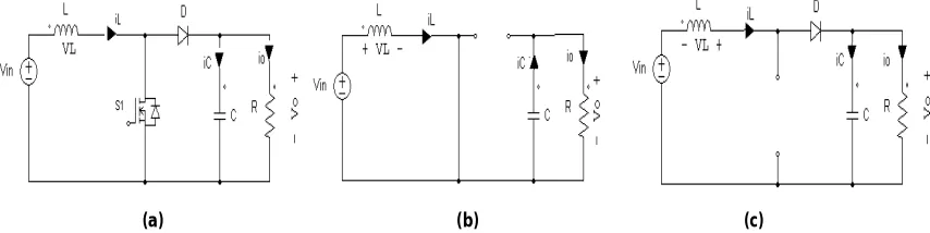
The operational circuit of Boost converter is shown in Fig.1 (a) Vin is source voltage, VL is the voltage across the inductor. Current iL, iC and io are flowing through the inductor, capacitor and resister respectively. D is a constant and Ts is time period. During the period DTs of a switching period S1 is ON and the inductor current iL flows from the input source to energize the inductor as shown in Fig.1(b) . During the period (1-D) Ts of a switching period S1 is OFF and the inductor current iL cannot change instantly as shown in Fig 1(c).The inductor current iL starts to decrease. This negative di/dt of the inductor current develops sufficient voltage (Ldi/dt) with a polarity such as to drive the inductor current through diode to charge the output capacitor [6].
(a) (b) (c)
Fig. 1. Circuit configuration of a boost converter: a)With operational switch b) ON-state, c) OFF-state.
A basic boost PFC rectifier converts a DC voltage to a higher DC voltage.The Interleave boost PFC rectifier does the same but it is consist of two single Boost converters connected in parallel so adds additional benefits with two output stages driven 180 degrees out of phase [7]. Conduction losses can be reduced by splitting the current into two power paths, which will result in gain of overall efficiency as compare to boost converter. Because the two phases are combined at the output capacitor, effective ripple frequency is doubled, making ripple voltage reduction much easier.
(a) (b)
(c) (d) (e)
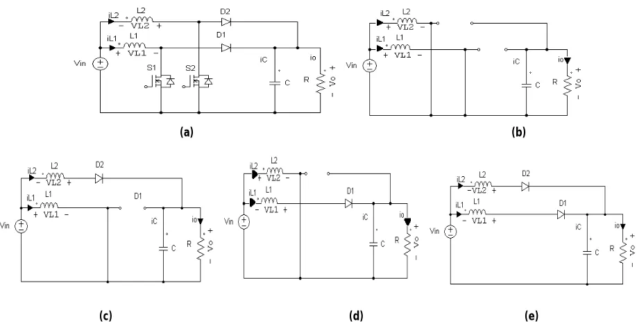
Fig. 2: Circuit configuration of a interleave boost converter a)With operational switch, b)S1andS2 on, c)S1 on and S2 off ,d)S1 off and S2 on ,e)S1 and S2 off
The state variables are assumed as inductor currents iL1 and iL2 and the capacitor voltage Vo. This converter comprises of four modes of operation.
1)Mode1:Switches S1 and S2 are on, diode D1 and D2 are off. At this stage, the state differential equations of the circuit are given by:
=
=
=−
⎣ ⎢ ⎢ ⎢ ⎡
⎦ ⎥ ⎥ ⎥ ⎤
=
0 0 0
0 0 0
0 0
+
0
(1)
2)Mode2:Switches S1 diode D2 are on, and S2 and D1 are off.
=
= −
= −
⎣ ⎢ ⎢ ⎢ ⎡
⎦ ⎥ ⎥ ⎥ ⎤
=
0 0 0
0 0
0
+
0
⎣ ⎢ ⎢ ⎢ ⎡ ⎦ ⎥ ⎥ ⎥ ⎤ = 0 0
0 0 0
0
+
0
(3)
4)Mode4:Switches S1 and S2 are off, diode D1and D2 are on.
= − = − = + − ⎣ ⎢ ⎢ ⎢ ⎡ ⎦ ⎥ ⎥ ⎥ ⎤ = ⎣ ⎢ ⎢ ⎢
⎡0 0
0 0 ⎦ ⎥ ⎥ ⎥ ⎤ + 0
(4)
III. CONTROLLERDESIGN
Fig. 3. Control scheme of the boost PFC with current control
The generated PWM is passed to turn on and off the boost converter switch. The PI controller ensures that the error at its input is zero, which implies that input current tracks reference current.
IV. EXPERIMENTAL VERIFICATION
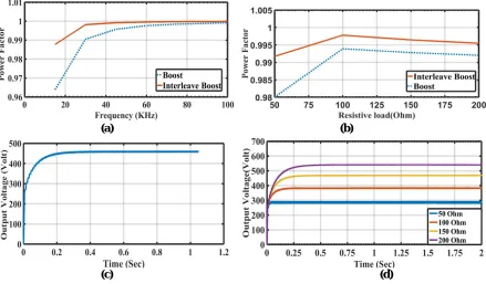
A 1500-W model is built in PSim to asses Boost control and IB control with PI current control method. The Input rms voltage is 220 V and the output voltage is 457V. The Power Factor (PF), Total harmonic Distortion (THD), Current and voltage ripple waveform under variable load and variable switching frequency in Boost and IB converter is shown in fig.4. Here AC input voltage is rectified by a diode bridge rectifier and then the rectified voltage is boosted using Interleave boost converter. It clearly shows that only input voltage and inductor current is sensed for the closed loop. Interleave converter is operated at 50kH frequency and pulse width is adjusted with the reference current value of 6.3A.
(a) (b)
(e) (f)
Figure 4. Simulation results: a) Variation of Power factor with switching frequency in boost and interleave boost; b) Power factor versus load of boost and interleave boost; c)Variation of output voltage with time in interleave boost converter; d) Plot of output voltage versus time at different loads in interleave boost converter; e) Steady state current waveform of Interleave boost converter ; f) Fast Fourier transform of ripple current in interleave boost converter.
The turn off time is determined by the time at which the average inductor current reaches a reference current limit. This involves an inner fast current control loop. The curve of Power factor versus frequency is shown in fig.4(a). Each switch operates at 50 kHz and total switching frequency is 100 kHz for Interleave Boost converter. It is observed that power factor increases with the switching frequency. The close observation shows that boost converter power factor is 0.9976 at 100 kHz. The interleave boost converter exhibits 0.9995 power factor at same switching frequency. Similar kind of results is also achieved in [4] with cascade control loop. The variation of Power factor of Boost and Interleave Boost converter is shown in fig.4(b). At maximum load of 100Ω power factor for boost converter is 0.9977 and for interleave boost converter it is 0.9992. Fig 4(c) shows the waveform for Boost converter’s output voltage. Vout is maintained to a constant value of 457V and output voltage ripple is up to 2%.Variation of ripple under load 50kΩ,100kΩ,150kΩ,200kΩ load is shown in Fig 4(d).Input current ripple of IB converter with FFT transform is shown in Fig.4(e),(f). Fundamental component is of 3.072A with current ripple of 0.731 A.
V.CONCLUSION
The average PI current controlled closed loop for boost and interleave boost converter is described, analyzed and compared. The fundamental issues Power factor correction, Output voltage regulation, Total Harmonic Distortion, Output voltage ripple and inductor current ripple is discussed. Frequency spectrum of the input current is shown. The comparative study of two topologies show the superior performance of the interleave boost converter. The result allows continuing future works in IB with a current loop or a cascade control using an adaptive control approach.
VI.ACKNOWLEDGMENT
This work has been supported by DST-PURSE, Savitribai Phule Pune University. One of the authors R.Rashmi is thankful to University Grant commission for JRF.
REFERENCES
[1] R.C Dugan, M.F Mcgranaghan, S Santoso, H.W Beaty, Electrical power system quality 2nd edition McGraw Hill New York 2002.
[2] M.H.J Bollen, “Understanding power quality problems “voltage sags an Interruptions”. IEEE Press New York 2000. [3] M. Rashid. ”Power Electronics Handbook”, 2nded,Prentice- Hall,2001,pp.167-185.
[4] M.Arun Devil, K.Valarmathi, R.Mahendran;" Ripple Current Reduction in Interleaved Boost converter by Using Advanced PWM Techniques",IEEE International Conference on Advanced Communication Control and Computing Technologies (lCACCCT), 2014. [5] Burak Akın “Comparison of Conventional and Interleaved PFC Boost Converters for Fast and Efficient Charge of Li-ion Batteries Used in
Electrical Cars”.2012 International Conference on Power and Energy Systems Lecture Notes in Information Technology, Vol.13
[7] Vaddi Ramesh, U. Haribabu, “Simulate the implementation of interleaved boost converter with zero voltage transition,” International Journal of Engg Research and Applications, vol.2, no.6, pp.1129-1135, Nov-Dec.2012.
[8] B. Lu, R. Brown, and M. Soldano, “Bridgeless PFC implementation using one-cycle control technique,” in Proc. IEEE Appl. Power Electron. Conf., 2005, pp. 812–817.
[9] Sun, J.; Bass, R.M.; , “Modeling and practical design issues for average current control,” in proc. IEEE APEC 1999, vol.2, pp.980-986 , 14-18 Mar 1999