Implementation of PRPG with Low Transition Test
Compression Technique for Low Power Applications
*K.SUSHMA
*M.SANJAY
M.TECH Dept of ECE, VAAGDEVI ENGINEERING COLLEGE
Asst prof Of .Dept of ECE, VAAGDEVI ENGINEERING COLLEGE
ABSTRACT:
The main challenging areas in VLSI are
performance, cost, testing, area, reliability
and power. The demand for portable
computing devices and communication
system are increasing rapidly. These
applications require low power dissipation
for VLSI circuits The novel test pattern
generator which is more suitable for built in
self test (BIST) structures used for testing of
VLSI circuits. This paper describes a
low-power (LP) programmable generator capable
of producing pseudorandom test patterns
with desired toggling levels and enhanced
fault coverage gradient compared with the
best-to-date built-in self-test (BIST)-based
pseudorandom test pattern generators. It is
comprised of a linear finite state machine (a
linear feedback shift register or a ring
generator) driving an appropriate phase
shifter, and it comes with a number of
features allowing this device to produce
binary sequences with preselected toggling
(PRESTO) activity.
We introduce a method
to automatically select several controls of
the generator offering easy and precise
tuning. The same technique is subsequently
employed to deterministically guide the
generator toward test sequences with
improved fault-coverage-topattern- count
ratios. Furthermore, this paper proposes an
LP test compression method that allows
shaping the test power envelope in a fully
predictable, accurate, and flexible fashion by
adapting the PRESTO-based logic BIST
(LBIST) infrastructure.
1. INTRODUCTION:
The main challenging areas in VLSI are
performance, cost, and power dissipation.
Due to switching i.e. the power consumed
testing, due to short circuit current flow and
charging of load area, reliability and power.
The demand for portable computing devices
and communications system are increasing
rapidly. These applications require low
power dissipation VLSI circuits. The power
than in normal mode. Hence it is important
aspect to optimize power during testing.
Power optimization is one of the main
challenges. Although over the next years,
the primary objective of manufacturing test
will remain essentially the same to ensure
reliable and high quality semiconductor
products—conditions and consequently also
test solutions may undergo a significant
evolution.
The semiconductor technology, design
characteristics, and the design process are
among the key factors that will impact this
evolution. With new types of defects that
one will have to consider to provide the
desired test quality for the next technology
nodes such as 3-D, it is appropriate to pose
the question of what matching
design-for-test(DFT) methods will need to be deployed.
Test compression, introduced a decade ago,
has quickly become the main stream DFT
methodology. However, it is unclear
whether test compression will be capable of
coping with the rapid rate of technological
changes over the next decade.
Interestingly, logic built-in self-test
(LBIST), originally developed for board,
system, and in-field test, is now gaining
acceptance for production test as it provides
very robust DFT and is used increasingly
often with test compression. This hybrid
approach seems to be the next logical
evolutionary step in DFT. It has potential for
improved test quality; it may augment the
abilities to run at-speed power aware tests,
and it can reduce the cost of manufacturing
test while preserving all LBIST and scan
compression
advantages. Attempts to overcome the
bottleneck of test data bandwidth between
the tester and the chip have made the
concept of combining LBIST and test data
compression a vital research and
development area. Thorough surveys of
relevant test compression techniques can be
found, for example, As with conventional
scan-based test, hybrid schemes, due to the
high data activity associated with scan-based
test operations, may consume much more
power than a circuit under test was designed
to function under. With overstressing
devices beyond the mission mode,
reductions in the operating power of ICs in a
test mode have been of concern for years.
Full toggle scan patterns may draw several
times the typical functional mode power,
and this trend continues to grow, particularly
over the mission mode’s peak power.
2. PROJECT DESCRIPTION:
The test pattern generator produces test
vectors that are applied to the tested circuit
combinational circuits. The nature of the
generator thus directly influences the fault
coverage achieved. the influence of the type
of pseudo-random pattern generator on
stuck-at fault coverage. Linear feedback
shift registers (LFSRs) are mostly used as
test pattern generators, and the generating
polynomial is primitive to ensure the
maximum period. We have shown that it is
not necessary to use primitive polynomials,
and moreover that their using is even
undesirable in most cases. This fact is
documented by statistical graphs.
The necessity of the proper choice of a
generating polynomial and an LFSR seed is
shown here, by designing a mixed-mode
BIST for the ISCAS benchmarks as the
complexity of VLSI circuits constantly
increases, there is a need of a built-in
self-test (BIST) to be used. Built-in self-self-test
enables the chip to test itself and to evaluate
the circuit’s response. Thus, the very
complex and expensive external ATE
(Automatic Test Equipment) may be
completely omitted, or its complexity
significantly reduced. Moreover, BIST
enables an easy access to internal structures
of the tested circuit, which are extremely
hard to reach from outside. There have been
proposed many BIST equipment design
methods. In most of the state-of-the-art
methods some kind of a pseudorandom
pattern generator (PRPG) is used to produce
vectors to test the circuit. These vectors are
applied to the circuit either as they are, or
the vectors are modified by some additional
circuitry in order to obtain better fault
coverage. Then the circuit’s response to
these vectors is evaluated in a response
analyzer. Usually, linear feedback shift
registers (LFSRs) or cellular automata (CA)
are used as PRPGs, for their simplicity.
Patterns generated by simple LFSRs or CA
often do not provide a satisfactory fault
coverage. Thus, these patterns have to be
modified somehow. One of the method that
is designing low power lfsr that can perform
fault analysis and reduce the power of a
circuit during test by generating three
intermediate patterns between the random
patterns by reducing the hardware
utilization.
The goal of having intermediate patterns is
to reduce the transitional activities of
Primary Inputs (PI) which eventually
reduces the switching activities inside the
Circuit under Test (CUT) and hence power
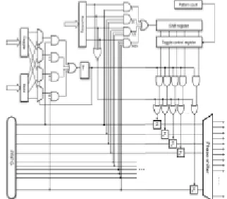
consumption is also reduced An n-bit PRPG
connected with a phase shifter feeding scan
chains forms a kernel of the generator
producing the actual pseudorandom test
ring generator can implement a PRPG. More
importantly, however, n hold latches are
placed between the PRPG and the phase
shifter. Each hold latch is individually
controlled via a corresponding stage of an
n-bit toggle control register. As long as its
enable input is asserted, the given latch is
transparent for data going from the PRPG to
the phase shifter, and it is said to be in the
toggle mode.
When the latch is disabled, it captures and
saves, for a number of clock cycles, the
corresponding bit of PRPG, thus feeding the
phase shifter (and possibly some scan
chains) with a constant value. It is now in
the hold mode. It is worth noting that each
phase shifter output is obtained by XOR-ing
outputs of three different hold latches.
Therefore, every scan chain remains in a
low-power mode provided only disabled
hold latches drive the corresponding phase
shifter output the toggle control register
supervises the hold latches. Its content
comprises 0s and 1s, where 1s indicate
latches in the toggle mode, thus transparent
for data arriving from the PRPG. Their
fraction determines a scan switching
activity. The control register is reloaded
once per pattern with the content of an
additional shift register. The enable signals
injected into the shift register are produced
in a probabilistic fashion by using the
original PRPG with a programmable set of
weights. The weights are determined by four
AND gates producing 1s with the
probability of 0.5, 0.25, 0.125, and 0.0625,
respectively.
The OR gate allows choosing probabilities
beyond simple powers of 2. A 4-bit register
Switching is employed to activate AND
gates, and allows selecting a user-defined
level of switching activity. Given the phase
shifter structure, one can assess then the
amount of scan chains receiving constant
values, and thus the expected toggling ratio.
While preserving the operational principles
of the basic solution, this approach splits up
a shifting period of every test pattern into a
sequence of alternating hold and toggle
intervals. To move the generator back and
forth between these two states, we use a
T-type flip-flop that switches whenever there
is a 1 on its data input. If it is set to 0, the
generator enters the hold period with all
latches temporarily disabled regardless of
the control register content. This is
accomplished by placing AND gates on the
control register outputs to allow freezing of
all phase shifter inputs.
This property can be crucial in SoC designs
where only a single scan chain crosses a
cause locally unacceptable heat dissipation
that can only be reduced due to temporary
hold periods. If the T flip-flop is set to 1 (the
toggle period), then the latches enabled
through the control register can pass test
data moving from the PRPG to the scan
chains. Two additional parameters kept in
4-bit Hold and Toggle registers determine how
long the entire generator remains either in
the hold mode or in the toggle mode,
respectively.
To terminate either mode, a 1 must occur on
the T flip-flop input. This weighted
pseudorandom signal is produced in a
manner similar to that of weighted logic
used to feed the shift register. The T
flip-flop controls also four 2-input multiplexers
routing data from the Toggle and Hold
registers. It allows selecting a source of
control data that will be used in the next
cycle to possibly change the operational
mode of the generator .For example, when
in the toggle mode, the input multiplexers
observe the Toggle register. Once the
weighted logic outputs 1,the flip-flop
toggles, and as a result all hold latches
freeze in the last recorded state. They will
remain in this state until another 1 occurs on
the weighted logic output. Th event is now
related to the content of the Hold register,
which determines when to terminate the
hold mode.
A n-bit PRPG is connected with a phase
shifter feeding scan chains producing
pseudo random test patterns. A linear
feedback shift register (LFSR) or a ring
generator can implement a PRPG. In
between PRPG and phase shifter n hold
latches are connected and it is controlled by
n-bit toggle control register. When the
enable input is given, the latch becomes
transparent otherwise latch is disabled and
captures and saves for a period of clock
cycles with constant value feeding phase
shifter.
The toggle control registers supervises hold
latches which consists of 0s and 1s where 1s
indicate toggle mode thus latch is
transparent for data moving from PRPG.
The toggle control register are loaded once
per pattern count with additional shift
register content and the enable signals for
the shift register are produced in probalisitic
manner by using original PRPG with
programmable set of weights. The weights
are determined by four AND gates
producing 1s with probability
0.5,0.25,0.125,0.0625 respectively. the OR
gate allows choosing probabilities beyond
Fig1:Operational version of PRESTO generator
An additional 4-input NOR gate detects the
switching code0000, which is used to switch
the LP functionality off.So,while working in
weighted random mode,the switching
selector ensures stastically stable content of
the control register interms of amount of 1s
it carries.Much higher flexibility in forming
low-toggling test patterns can be achieved
using this architecture.This approach splits
up a shifting period of every test pattern into
sequence of alternate toggle and hold
intervals.To move to and forth between
toggle and hold states,we use a T-flip flop
that switches wheneverthere is at 1 on its
data input.If it is set to 0,the generator enters
in hold mode with temporarily disabling
latches regardless of the toggle control
register.If it is set to 1,it enables the latches
and enters into togglemode which moves
data from PRPG to scan chains.
Two additional parameters kept in toggle
and hold register determine how long the
entire generator remains either in toggle or
hold mode. To terminate either mode, a
1must occur on T-flip flop similar to that of
a weighted logic used to feed the shift
register. The T-flip flop controls four
2-input multiplexers routing data from toggle
and control registers. It allows selecting a
source of control data that will be used in
the next cycle to change the operational
mode of the generator. Test patterns. When
using the PRESTO generator with existing
DFT flow, all LP registers are either loaded
once per test data registers or parts of an
IJTAG network, and are initialized by the
test setup procedure.Clearly,it suits LBIST
applications where shift speeds are quite
high.As shown in operational version of
PRESTO generator depend on mainly three
factors in BIST mode they are:1)1the
switching code(kept in switching register
2)the hold duty cycle(HC) 3)the toggle duty
cycle.Given the size of PRPG,the number of
the scan chains and the corresponding phase
shifter, the switching code as well as HC
and TC values can be selected automatically
in such a way that the entire generator will
produce pseudorandom test patterns having
a desired level of togglingT provided the
scan chains are balanced.The procedure for
selecting these parameters consists of many
toggle codes yields a ratio r with smallest
deviation from theoretical values using
equation A=(T * S)/50 where S is the total
number of scan chains and T is the toggling
level (%) and A is the number of active scan
chains.
Ring generators are high performance LFSR
which produces pseudo random test patterns
which produces binary sequences. Two
adjacent flip flop contain atmost one 2-input
XOR gate and each flip-flop output drives
atmost 2 fanoutnodes. The circuit is
constructed in ring structure so there is no
long feedback path connecting the right
most flipflop to the left-most flip flop. It is a
ring shape structure and produces two layer
feedback so power consumption will be
more. The principle of the decompressor is
to disable both weighted logic blocks(V and
H) and to deploy control data instead. The
content of toggle control register can be
selected in deterministic manner due to
multiplexer placed in front of shift register.
Further, the toggle and hold registers
alternately preset a 4-bit down counter, thus
determine the durations of hold and toggle
phases. When circuit reaches a value of
zero, it causes a dedicated signal to go high
in order to toggle the T-flip flop. The same
signal allows the counter to have the input
data kept in toggle or hold register entered
as the next state.
Both the down counter and the T-flip flop
needed to be initialized for every test
pattern.The initial value to the T- flip flop
decides whether the decompressor will
begin to operate either in toggle or in the
hold mode, while the initial value to the
counter is reffered to as an offset,
determines mode’s duration.The
functionality of the T-flip flop remains same
as that of LP PRPG.Here, it occurs in two
cases: First of all, the encoding procedure
can completely disable the hold phase by
loading the Hold register with appropriate
code.If detected (No Hold) it overrides the
output of the T-flip flop by using an
additional OR gate.As a result, the entire test
pattern is going to be encoded within toggle
mode exclusively.In addition ,all the hold
latches have to be properly initialized.Hence
a contro signal First cycle produced at the
end of ring generator initialization phase
reloads all latches with current content of
this part of the decompressor.
In order to facilitate test data decompression
while preserving its original functionality
the circuit is rearchitected.This architecture
consists of an additional block transition
controller and ring generator is replaced by
patterns and consumes less power compared
to ring generator.Transition controller
produces less controlled transitions on phase
shifter outputs. In the proposed system,
Linear feedback shift registers(LFSRs)
produce extremely good pseudorandom test
patterns.Gated clock signal present in design
approach for LFSR lead to power
reduction.Power reduction hardly depends
on technological characteristic of gates
employed.
LFSR is a shift register whose input isresult
of XOR of some of its inputs.The outputs of
flip-flops are loaded with seed
value(anything except 0s which cause LFSR
to produce all 0 patterns)and when LFSR is
clocked,it will generate PRPG of 1s and
0s.Here,the signal necessary to generate test
patterns is clock.Maximum length of LFSR
is 2^n-1.
Fig.2: Simplified circuit of a generic LFSR circuit
Low Power PRPG architecture with transition controller:
Fig 3: Low power PRPG with transition controller
An adaptive technique is applied to reduce
the shift power to improve the shift power
reduction in logicBIST.To get the required
power reduction, we implement an
additional module called transition
controller.During shift mode the previous
test responses in scan flip-flops are given as
feedback to transition controller which is
used to generate test patterns so that
switching is reduced. The transition
controller consists of a multiplexer,a XNOR
gate and D-flip flop.The inputs of XNOR
gate is driven by the outputs of last two scan
cells in the same chain SCk-1 and SCk.
The output of XNOR gate connects to
multiplexer selects input and here,we
assume that there is no inversion between
different values ,the value at XNOR gate
output is 0 and it causes the D-flip flop hold
its previous value.Otherwise the D-FF will
be updated by phase-shifter output.
3 RESULTS:
The design proposed in this paper has been
developed using MODEL SIMULATOR
Fig 4: Simulation result of Low power PRPG with transition controller
4 CONCLUSION & FUTURE SCOPE: A low power test pattern generator has been
proposed which consists of a modified low
power linear feedback shift register
(LP-LFSR). The seed generated from (LP-LFSR)
is Ex-ORed with the single input changing
sequences generated from gray code
generator, which effectively reduces the
switching activities among the test patterns.
Thus the proposed method significantly
reduces the power consumption during
testing mode with minimum number of
switching activities using LP-LFSR in place
of conventional LFSR in the circuit used for
test pattern generator. From the
implementation results, it is verified that the
proposed method gives better power
reduction compared to the exiting method.
REFERENCES:
[1] BalwinderSingh, Arun khosla and
Sukhleen Bindra “Power Optimization of
linear feedback shift register(LFSR) for low
power BIST” , 2009 IEEE international
Advance computing conference(IACC
2009) Patiala,India 6-7 March 2009.
[2] Y.Zorian, “A Distributed BIST control scheme for complex VLSI devices,” Proc.
VLSI Test Symp., P.4-9,1993.
[3] P.Girard,” survey of low-power testing of VLSI circuits,” IEEE design and test of
computers, Vol. 19,no.3,PP 80-90,May-June
2002.
[4] Mechrdad Nourani,”Low-transition test
pattern generation for BIST- Based
Applications”, IEEE TRANSACTIONS ON
COMPUTERS, Vol57,No.3 ,March 2008.
[5] BOYE and Tian-Wang Li,” A novel
BIST scheme for low power testing,” 2010
IEEE.
[6] R.S.Katti,X.Y.Ruan , and H.Khattri,”
Multiple-Output Low-Power Linear
feedback shift register design,”
IEEETrans.circuitsSyst.I,Vol.53,No.7,pp-
[7] P.Girard, L.Guiller, C.Landrault,
S.Pravossoudovitch,and H.J.Wunderlich,” A
modified clock scheme for a low power
BIST test pattern generator,” 19th IEEE
proc. VLSI test Symp.,CA,pp-306-
311,Apr-May 2001.
[8] S.Wang and S.K.Gupta,” DS-LFSR: a BIST TPG for low switching activity,” IEEE
Trans.computer-aided design of Integrated
circuits and systems, Vol.
21,No.7,pp.842-851,July 2002.
[9] I.Voyiatzis,A.paschalis,D.Nikolos and
C.Halatsis, ”An efficient built-in self test method for robust path delay fault testing,”
Journal of electronic testing: Theory and
applications Vol.8,No.2,pp-219-222,Apr-
1996.
[10] S.C.Lei, J.Guo, L.Cao, Z.Ye.Liu, and
X.M.Wang,”SACSR: A low power BIST
method for sequential circuits,: Academic
Journal of XI’AN
jiaotonguniversity(EnglishEdition),Vol.20,n
o.3,pp.155- 159,2008.
AUTHOR 1:-
* K.SUSHMA completed her B tech
in Pathfinder Engineering College
and pursuing M-
Tech in Vaagdevi Engineering
College
AUTHOR 2:-
** M.SANJAY is working as
Assistant Professor in Dept of ECE,
Vaagdevi
Engineering College