Design of a Pipelined 32 Bit MIPS Processor
with Floating Point Unit
P Ajith Kumar 1, M Vijaya Lakshmi 2
P.G. Student, Department of Electronics and Communication Engineering, St.Martin’s Engineering College,
Hyderabad, Telangana, India1
Associate Professor, Department of Electronics and Communication Engineering, St.Martin’s Engineering College,
Hyderabad, Telangana, India2
ABSTRACT: The aim of the work is to design and implementation of 32 bit MIPS processor. The architecture with
pipelined control RISC core consists of fetch, decode, execute, pipeline control and memory. The reduction in the power is achieved using HDL modification techniques. The design is based on program counter, instruction memory, logical unit, arithmetic unit and optimization techniques.
KEYWORDS:32bit RISC, MIPS.
I.INTRODUCTION
Present era of SOC’s comprise analog, digital and mixed signal components housing on the same chip. In this environment processor plays a vital role. As the technology shrinking to sub-micrometer technology node, there exists a huge-scope of undesirable hazards in processors. These hazards may lead to disturbance in area, power and timing which deviate from desired quantities. Our paper focuses mainly to solve some of these issues. In-order to tackle these problems, we are introducing the enhanced version of MIPS. Microprocessor without interlocked pipeline stages (MIPS) is a recent architecture into the semi-conductor industry. This paper totally concentrates on designing the architecture in Verilog HDL.
This paper describes a 32-bit MIPS processor core, based on the 5-stage pipelined RISC architecture [10]. The salient features of this 32 bit RISC core processor are its low power consumption due to the power optimization techniques utilized and high speed due to the 5-stage pipeline approach.
II. LITERATRE SURVEY
In literature survey, study was done on many optimization techniques related to RISC processor design. Some of the various optimization & low power techniques that were explored during the survey were power gating, clock gating, multi-voltage domain logical optimization etc. In this work, the various papers referred are as given below.
Neenu Joseph, Sabarinath S proposed a design for front end process to achieve reduced power [1]. In clock gating, the signal from the clock is prevented from reaching the various modules of the processor. In absence of the clock signal which prevents the register from changing their values. Overall power consumption is greatly reduced.
ISSN(Online) : 2319-8753 ISSN (Print) : 2347-6710
I
nternational
J
ournal of
I
nnovative
R
esearch in
S
cience,
E
ngineering and
T
echnology
(An ISO 3297: 2007 Certified Organization)
Vol. 5, Issue 7, July 2016
Development and testing of a microprocessor cell intended for very low power applications has been introduced by Adamec, F.,Fryza [4]. The internal architecture of the microprocessor cell is divided in two blocks: Control and Operational block. Clock gating techniques are used to implement a ‘Sleep’ block. These techniques put the processor in an extra low-power consumption state. This is carried out until awakened by an external interrupt. The Control block performs the opcode reading, decoding, and then controls the data flow in the Operation block in order to complete the operation. By studying the various papers it is observed that the work done was focused on techniques such as Wallace tree multiplier, clock gating, advanced branch technique, architectural techniques to reduce and optimize the overall power consumption. On the other hand, this paper proposes reduction in the total power consumption by HDL modification technique. The overall power optimization achieved by the HDL modification technique is 13.33%.
III.PROPOSEDTECHNIQUE
Design Implementation of 32bit RISC processor has Instruction decode, register bank, Instruction memory, execution unit and program counter. The program counter will generate address which data need to access from instruction memory. The data fetched from instruction memory is decoded in instruction decode, which generates read & write address for register bank. Based on the generated signals data is sent to execution unit, which writes back to register bank. Optimization and low power techniques can be designed without much complexity when the implementation technique is at the front end. Different types of optimization & low power techniques are used in this proposed architecture.
IV.RISCARCHITECTURE
In earlier designed MIPS architecture one of the key methods used to optimize the instructions set to complete in one clock cycle. Compilers were forced to insert "no-ops" in some cases. These cases where such as where the instruction takes longer than one clock cycle. Thus input and output activities (like memory accesses) specifically forced this behaviour. This architecture has a more advanced approach. Longer instructions were used in handling: data forwarding and instruction reordering. In this case the longer instructions are "stalled" in their functional units, and then reinserted into the instruction stream when they can complete.
Basic Architecture:
i. Instruction Fetch (IF) unit/cycle, IR<-Mem (PC), NPC<-PC+4:
Operation: This unit will fetch the instruction from memory. Later, this instruction is stored in the Instruction Register (IR). PC holds the address of memory location where instruction is written. PC is incremented by 4 so that its holds the address of next sequential instruction. The IR is used to hold the next instruction that will be needed on subsequent clock cycles.
ii. Instruction Decode (ID) unit:
Operation: this unit will decode the instruction in IR. Later the unit access the register file to read the registers. Instruction is fetched from IF and extracts Opcodes and operands from that instruction which intern retrieves register values.
iii. Execution unit/effective address (EX):
Fig. 1 Architecture of 32 bit RISC processor
Memory reference register either registers ALU instruction or register immediate ALU instruction branch. iv. Memory access unit (MEM):
The various active MIPS instructions which are active in the unit are as follows: loads, stores and branches. Memory reference: access memory if needed. If instruction is load, data returns from memory and is placed in the LMD (load memory data) register.
v. Write back (WB) unit:
This unit will hold the result in the register. Ideally, this unit refers to as the store unit. This unit writes or stores the result into a register.
V. INSTRUCTION SET OF MIPS PROCESOR
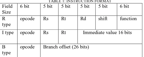
There are three types of instructions set i.e. R-type (register type), I-type (immediate type) and J-type (jump type). Register instructors are specified as R-type instructions. R-type consists of three register references contained in the 32-bit word. I-type instructions specify two registers. I-type instructions use 16 32-bits to hold an immediate value.
TABLE 1: INSTRUCTION FORMAT
Field Size
6 bit 5 bit 5 bit 5 bit 5 bit 6 bit
R type
opcode Rs Rt Rd shift function
I type opcode Rs Rt Immediate value 16 bits
B type
ISSN(Online) : 2319-8753 ISSN (Print) : 2347-6710
I
nternational
J
ournal of
I
nnovative
R
esearch in
S
cience,
E
ngineering and
T
echnology
(An ISO 3297: 2007 Certified Organization)
Vol. 5, Issue 7, July 2016
are used [7].Thus it allows the lower 6 bits to be used as "extended instructions". The RISC architecture supports 64 bit instructions, until all these instructions work purely on registers [8].
R type: In R type, bits 31-26 represent the opcode. Representation of the address of the first source register is from bits 25-21. Second source register is from bits 20-16. Destination register is from bits 15-11. Bits 10-6 correspond to the number of bits to be shifted. The final 6 bits 5-0 hold the functional core. This functional core correspond the ALU function.
I type: As with the R-type instruction the bits 31-26 corresponds the opcode. Bits 25-21 corresponds the address of the register at 1st source. Address of second source register is corresponded by bits 20-16. Finally, bit values from 15-0 of this I-type corresponds a 16 bit I-value given in 2’s complement form.
J-type: Opcode is given by bits 31-26. The type of branch operation to be performed is represented by this. Remaining last bits i.e. 26 bits i.e. ranging from 25 to 0 corresponds to the branch offset in 2’s complement format. To obtain the branch target address, this number is added to the value of the PC.
VI. OPTIMIZATION & LOW POWER TECHNIQUES
6.1 Power Management on Chip/FPGA: a) Battery life (in portable systems) b) Environmental concerns [5] c) Digital noise immunity d) Packaging and Cooling costs
6.2 Power Dissipation Sources: The power loss can be classified as described below:
a) Leakage power consumption: The dissipation of power occurs when system is idle/standby mode. b) Dynamic power consumption: Due to logic transitions of logic gates or flip-flops.
6.3 Low-Power Design Technique: The various layers at which the power reduction can be achieved are as listed below: a) Circuit Logic: Logic Styles, Energy Recovery, Transistor Sizing [9]
b) Architecture: Parallelism, Pipelining, Redundancy, Data Encoding c) Technology: Threshold Reduction, Multi-threshold devices d) System: Partitioning, Power down
e) Algorithm: Complexity, Concurrency, Regularity
The power reduction techniques are done based upon the changes in either Pipelining, Logic styles, Data Encoding. These various techniques will be explored to achieve power reduction.
6.4 Coding option using Verilog HDL to optimize power:
a) No reset is best since the FPGA gets a global reset automatically
b) Use low power architecting for multiple Block RAM arrays (use CORE generator) c) Only enable BRAM during active read or write cycles
d) Design with Synchronous Resets e) Minimize local resets, if possible
f) Build small memory blocks with LUTs (<4k bits) g) Control the use of Clock Enables [6]
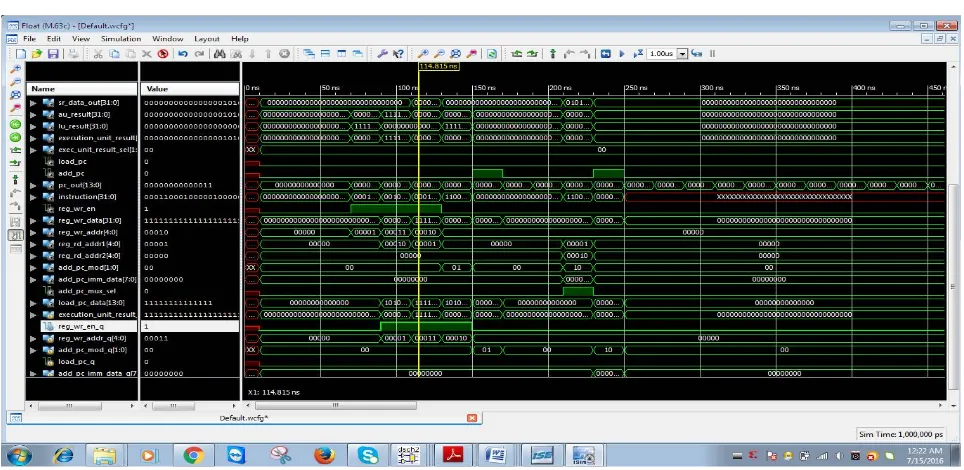
VII. RESULTS
Fig. 2 SIMULATION RESULT
VIII. CONCLUSION
Using RISC architecture, a 5 stage pipelined MIPS processor core is designed [9]. Following modules are developed: Fetch, Decode, ALU, Comparator, GPR Memory, Execute, Pipeline Control are designed. Using low power technique i.e. Verilog HDL modification a lower version of the processor is designed to reduce power consumption of the core. The overall power optimization achieved from HDL technique is 13.33%.
IX. FUTURE SCOPE
The above developed design can be reduced further using system partitioning. Consumption of the power can further be reduced at the manufacturing stage using techniques such as lithography.
REFERENCES
[1] Neenu Joseph, Sabarinath.S, Sankarapandiammala K ,“FPGA based Implementation of High Performance Architectural level Low Power 32-bitRISC Core”.
[2] Shofiqul Islam, Debanjan Chattopadhyay, Manoja Kumar Das, V Neelima; Rahul Sarkar, “Design of High Speed Pipelined Execution Unit of 32-bit RISC Processor” India Conference, Annual IEEE , pp. 1 - 5, 2006.
[3] Samiappa Sakthikumaran et al., “A Very Fast and Low Power Carry Select Adder Circuits”, 3rd International Conference on Electronics Computer Technology - ICECT 2011.
[4] Adamec, F.,Fryza, T., “Design and Optimization of ColdFire CPU Arithmetic and Logic Unit”, Proceedings of 16th International Conference on mixed design of integrated circuits & Systems, pp. 699 – 702, 2009.
[5] Xilinx, “Power Consumption in 65nm FPGAs,” 2007
[6] Xilinx, “Optimizing FPGA power with ISE design tools,” Xcell Journal, Issue 60, pp. 16-19, 2007.
[7] Patterson, David; Hennessy, John (1996). “Computer Architecture: A Quantitative Approach” (1st Ed.). Morgan Kaufmann. ISBN 978-1-55- 860329-5.
[8] Stephen B. Furber, "VLSI RISC Architecture and Organization", 2nd Edition CRC Press, pp. 24-28.