Image Processing using IP Core Generator through
FPGA
B.Muralikrishna
1K.Gnana Deepika
2B.Raghu Kanth
3V.G.Swaroop Vemana
4Assistant Professor, Department of ECE, K L University, Vaddeswaram, AP, India - 522 502
1G Student, Department of ECE, K L University Vaddeswaram, AP, India - 522 502.
2,3,4ABSTRACT
Xilinx CORE Generator System generates and delivers parameterizable cores optimized for Xilinx FPGAs. CORE Generator is mainly used to create high density, high performance designs in Xilinx FPGAs in less time. The CORE Generator is included with the ISE WebPack and ISE Foundation software and comes with an extensive library of Xilinx LogiCORE IP. These include DSP functions, memories, storage elements, math functions and a variety of basic elements. Xilinx provides a flexible Block Memory Generator core to create compact, high-performance memories running at up to 450 MHz. Block Memory Generator provides single port and dual port block memory. These memory types differ in selection of operating modes.Matlab tool is used to convert the image that is being processed to .coe file format. Xilinx Core Generator is used to store the coefficient file(.coe) in single port Block ROM by defining the width and depth of the image and image is displayed on VGA monitor using Digilent Nexys2 FPGA Board.
Keywords
Xilinx IP CORE Generator, VGA(Videos Graphics Array),Blocm Memory Generator ,Coefficient File
1.
INTRODUCTION
The Block Memory Generator LogiCORE™ IP core automates the creation of area and performance optimized block memories for Xilinx FPGAs. Available through the ISE® Design Suite CORE Generator™ System, the core enables users to create block memory functions to suit a variety of requirements. Built-in knowledge about XilBuilt-inx device architectures allow it to leverage specialized FPGA architectural features to create the most compact, high performance solution. The Block Memory Generator[1] core uses embedded Block Memory primitives in Xilinx FPGAs to extend the functionality and capability of a single primitive to memories of arbitrary widths and depths. Sophisticated algorithms within the Block Memory Generator core produce optimized solutions to provide convenient access to memories for a wide range of configurations.
The Block Memory Generator[2] has two fully independent ports that access a shared memory space. Both A and B ports have a Write and a Read interface. In Kintex-7, 7, Virtex-6, Virtex-5 and Virtex-4 FPGA architectures, each of the four interfaces can be uniquely configured with a different data width. When not using all four interfaces, the user can select a simplified memory configuration (for example, a Single-Port Memory or Simple Dual-Port Memory) to reduce FPGA resource utilization. The Block Memory Generator is not completely backward-compatible with the discontinued legacy
[image:1.595.310.536.304.442.2]Single-Port Block Memory and Dual-Port Block Memory cores. General system over view of Xilinx Core Generator is shown in the below figure:
Figure 1: Core Generator System Overview
1.1 Single Port BLOCK MEMORY
The Single-Port Block Memory module is generated based on the user-specified width and depth. This module for Spartan-II and Virtex is composed of single or multiple 4 Kb blocks called Select RAM+. The Virtex-II, Virtex-II Pro, Virtex-4, and Spartan-3 Single-Port Block Memory modules, on the other hand, are composed of single or multiple 18 Kb blocks called SelectRAM- II. Since Spartan-II and Virtex both use the 4 Kb SelectRAM+ blocks, any particular reference to a Virtex implementation also applies to a Spartan-II, Virtex-E, Virtex-II Pro, or Spartan-IIE implementation[3].
When Block Memory is enabled, all memory operations occur on the active edge of the clock input (CLK). The Block Memory can be configured to be active on the rising edge and the falling edge. When the block memory is disabled (enable inactive), the memory configuration and output value remain unaltered.
[image:1.595.359.500.654.742.2]During Write Operation(WE asserted), the data presented at the port’s data input is stored in memory at the location selected by the port’s address input.
1.2 Dual Port BLOCK MEMORY
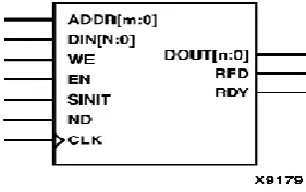
[image:2.595.320.538.68.215.2]The Dual Port Block RAM has two independent access ports that permit shared access to a central pool of memory. The data width and memory depth of each access port can be independently configured providing straightforward dual-port memory functionality or optional data formatting capability. Both ports are functionally identical, with each port providing read and write access[4]. Simultaneous reads from the same memory location may occur, but all other simultaneous, same location operations should be avoided. Simultaneously reading-from and writing-to the same location results in the correct data being written into the memory, but invalid data being presented at the reading port.
Figure 3: Core Schematic Symbol
2.
VGA(VIDEO GRAPHICS ARRAY)
The term Video Graphics Array (VGA) refers either to an analog computer display standard, the 15-pin D-subminiature VGA connector, or the 640×480 resolution itself. VGA is referred to as an "array" instead of an "adapter" because it was implemented from the beginning as a single chip, replacing the Motorola 6845 and dozens of discreet logic chips covering a full-length ISA board that the MDA,CGA, and EGA used. This also allowed it to be placed directly on a PC's motherboard with a minimum difficulty (it only required video memory, timing crystals and an external RAMDAC).
2.1 vga display port
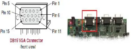
The Spartan-3E FPGA Starter Kit board includes a VGA display port via a DB15 connector. Connect this port directly to most PC monitors or flat-panel LCDs using a standard monitor cable. The VGA connector is the left-most connector along the top of the board as shown in the below figure.
[image:2.595.112.251.264.381.2]Figure 4: Core Schematic Symbol
Figure 5: VGA Connections from Spartan-3E Starter Kit Board
[image:2.595.322.546.349.498.2]The Spartan-3E FPGA directly drives the five VGA signals via resistors. Each color line has a series resistor, with one bit each for VGA_RED, VGA_GREEN, and VGA_BLUE. The series resistor, in combination with the 75Ω termination built into the VGA cable, ensures that the color signals remain in the VGA-specified 0V to 0.7V range. The VGA_HSYNC and VGA_VSYNC signals using LVTTL or LVCMOS33 I/O standard drive levels[5]. Drive the VGA_RED, VGA_GREEN, and VGA_BLUE signals High or Low to generate the eight colors as shown in the below table.
Figure 6: 3-bit display color codes
2.2 Signal timing for 60hz,640x480 VGA
Display
CRT-based VGA displays use amplitude-modulated, moving electron beams (or cathode rays) to display information on a phosphor-coated screen. LCDs use an array of switches that can impose a voltage across a small amount of liquid crystal, thereby changing light permittivity through the crystal on a pixel-by-pixel basis. Although the following description is limited to CRT displays, LCDs have evolved to use the same signal timings as CRT displays. Consequently, the following discussion pertains to both CRTs and LCDs.
[image:2.595.69.281.594.676.2]Figure 7: CRT display Timing Example
information is only displayed when the beam is moving in the forward direction—left to right and top to bottom—and not during the time the beam returns back to the left or top edge of the display. Much of the potential display time is therefore lost in blanking periods when the beam is reset and stabilized to begin a new horizontal or vertical display pass.
Modern VGA displays support multiple display resolutions, and the VGA controller dictates the resolution by producing timing signals to control the raster patterns. The controller produces TTL-level synchronizing pulses that set the frequency at which current flows through the deflection coils, and it ensures that pixel or video data is applied to the electron guns at the correct time.
The VGA controller generates the horizontal sync (HS) and vertical sync (VS) timings signals and coordinates the delivery of video data on each pixel clock. The pixel clock defines the time available to display one pixel of information. The VS signal defines the refresh frequency of the display, or the frequency at which all information on the display is redrawn. The minimum refresh frequency is a function of the display’s phosphor and electron beam intensity, with practical refresh frequencies in the 60 Hz to 120 Hz range. The number of horizontal lines displayed at a given refresh frequency defines the horizontal retrace frequency.
3.
EXPERIMENTAL SETUP
3.1 IP core generator
The core generation process produces the logic for the core, partitions it into configurable logic blocks (CLBs), and then places the CLBs relative to each other. This logic design coupled with a CLB-floor-plan or physical design is what makes our cores predictable. The relative locations are maintained as the core is integrated into the overall design and placed anywhere in a large FPGA[6].
Figure 8: Xilinx IP core Design Flow
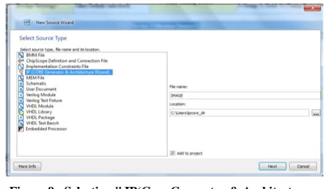
The CORE Generator contains a library of LogiCORE parameterizable cores, AllianceCORE cores, and data sheets. The LogiCORE category contains cores that are designed and supported by Xilinx, while the AllianceCORE category contains the cores that are designed and supported by our AllianceCORE partners. The "IP(Core Generator & Architecture wizard) can be launched from ISE as shown in th below figure:
STEP BY STEP IP CORE INITIALIZATION PROCEDURE FOR LOADING COE FILE IN BRAM
Figure 9: Selecting " IP(Core Generator & Architecture wizard) " from ISE
[image:3.595.72.274.77.284.2]"Block Memory Generator" is one of the IP core that is provided by the Xilinx IP Core Generator which is present under the "Memory and Storage Element".
[image:3.595.317.549.358.493.2]The following Procedure is followed in order to select ""Block Memory Generator”:
Figure 11: Selection of "Block memory Generator" IP core
[image:4.595.53.274.95.270.2]3.2 BLOCK Memory generator
Figure 12: "Block memory Generator" IP core Wizard
Block Memory Generator wizard is launched showing different memory types and IP Symbol."Single Port ROM" is selected under memory types and the values for read width and read depth are specified based on horizontal width and vertical length of the Image that is being processed.
After defining all of your parameters, simply click on the Generate button. The output is an optimized CORE for the targeted FPGA device with the following files.
A tailored Xilinx netlist with complete relative placement information to guarantee performance VHDL or Verilog instantiation code
A VHDL behavioral model
[image:4.595.53.289.310.473.2] A symbol for schematic capture tools
Figure 13: "Block memory Generator" IP core Wizard
3.3 Coefficient File Format(.coe)
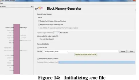
[image:4.595.306.549.324.465.2]coe file stands for Coefficient file that contains the contents of the Block Memory for the specified read depth and read width values of the image. The size of the image that is available is 640x480 and this data is stored as .coe file in single port Block ROM using Xilinx Core Generator. Matlab function IMG2coe8(imgfile, outfile)[7] is used to convert bmp,jpeg,png,gif and tif image file formats to .coe file format.
Figure 14: Initializing .coe file
Click Next for further steps and click "Generate" button in Block Memory Generator wizard and the message that the "IP core successfully created " is shown in the Xilinx ISE environment.
[image:4.595.320.552.508.656.2]4.
RESULTS
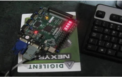
[image:5.595.330.532.113.313.2]4.1 Initial Set up of Hardware and the
Output
Figure 16: Digilent Nexys2 FPGA Board with VGA cable connected Through Serial (RS-232) Communication
The original image read into the Matlab function will contain 8-bits of red, 8-8-bits of green, and 8-8-bits of blue. The 8-bit color byte stored in the .coe file will contain only the upper 3 bits of red, the upper 3 bits of green, and the upper 2 bits of blue. This is done because, the Nexys-2 board supports only 8-bit VGA colors.
Figure 17: Original Image
[image:5.595.55.292.134.284.2]The resulting 8-bit color image will be of reduced quality from the original image as can be seen in below figure:
Figure 18: Image After processing through Core Generator
5.
CONCLUSION
To increase software development productivity, efficient code reuse is important. With field-programmable gate array (FPGA) hardware, reusable code blocks often called IP blocks are created. Xilinx Core Generator provides such flexibility to create IP cores for high performance memories. Block Memory Generator is one of the IP core that is provided by Xilinx Core Generator which allows to store larger images. Matlab tool is used to convert image of any type to .coe file format and is stored in Single Port BLOCK ROM.The data in .coe file is read and the IP core is successfully created in Xilinx ISE environment. The top level design in ISE is synthesized and download.bit file is loaded into Digilent Nexys2 FPGA Board and is displayed on VGA monitor.
6.
REFERENCES
[1] http://www.xilinx.com/ise/products/coregen_overview.pdf
[2] http://www.xilinx.com/support/documentation/ip_documen tation/sp_block_mem.pdf
[3] http://www.xilinx.com/support/documentation/ip_documen tation/sp_block_mem.pdf
[4] http://www.nalanda.nitc.ac.in/industry/appnotes/xilinx/docu ments/dsp/docs/mem_dp_block.pdf
[5] Xilinx Inc., Spartan-3e FPGA starter kit Board user guide
[6] http://www.xilinx.com/tools/coregen.htm
[image:5.595.95.268.402.623.2]