Scholarship at UWindsor
Scholarship at UWindsor
Electronic Theses and Dissertations Theses, Dissertations, and Major Papers
4-14-2017
An FPGA Implementation of a Custom JPEG Image Decoder SoC
An FPGA Implementation of a Custom JPEG Image Decoder SoC
Module
Module
George Gabriel Kyrtsakas University of Windsor
Follow this and additional works at: https://scholar.uwindsor.ca/etd
Recommended Citation Recommended Citation
Kyrtsakas, George Gabriel, "An FPGA Implementation of a Custom JPEG Image Decoder SoC Module" (2017). Electronic Theses and Dissertations. 5945.
https://scholar.uwindsor.ca/etd/5945
JPEG Image Decoder SoC Module
by
George Kyrtsakas
A Thesis
Submitted to the Faculty of Graduate Studies through the
Department of Electrical and Computer Engineering in Partial Fulfillment
of the Requirements for the Degree of Master of Applied Science at the
University of Windsor
All Rights Reserved. No Part of this document may be reproduced, stored or
oth-erwise retained in a retrieval system or transmitted in any form, on any medium by
by
George Kyrtsakas
APPROVED BY:
B.Boufama Computer Science
M.Khalid
Electrical and Computer Engineering
R.Muscedere, Advisor
Electrical and Computer Engineering
I hereby declare that this thesis incorporates material that is result of joint research,
as follows: the Verilog code presented in Appendix A is the outcome of a joint effort
between myself, George Kyrtsakas, and my supervisor, Dr. Roberto Muscedere.
I am aware of the University of Windsor Senate Policy on Authorship and I certify
that I have properly acknowledged the contribution of other researchers to my thesis,
and have obtained written permission from each of the co-author(s) to include the
above material(s) in my thesis.
I certify that, with the above qualification, this thesis, and the research to which
it refers, is the product of my own work.
I declare that, to the best of my knowledge, my thesis does not infringe upon
anyones copyright nor violate any proprietary rights and that any ideas, techniques,
quotations, or any other material from the work of other people included in my
thesis, published or otherwise, are fully acknowledged in accordance with the standard
referencing practices. Furthermore, to the extent that I have included copyrighted
material that surpasses the bounds of fair dealing within the meaning of the Canada
owner(s) to include such material(s) in my thesis.
I declare that this is a true copy of my thesis, including any final revisions, as
approved by my thesis committee and the Graduate Studies office, and that this thesis
An important feature of today’s mobile devices is their ability to capture and display
high resolution photos in an acceptable time frame. The vast majority of images are
stored on disk using the JPEG codec for compression. With increasing pixel counts
on both image sensors and screens, software solutions will struggle in their ability to
decode JPEG image data, since they rely solely on increasing CPU power. The need
is becoming clearer for hardware acceleration to replace the CPU when decoding large
images.
This thesis presents a System-on-Chip module that is able to relieve the CPU of
the computationally intense task of decoding a JPEG image. This SoC module was
developed and tested on an FPGA that features an ARM Cortex A9 and a Xilinx
Artix–7 FPGA. The SoC module was able to outperform software running on the
To my family, this work is the culmination of twenty-four and a half years of continual
love and support from you. This is as much your achievement as it is mine. Thank
I would like to thank my Supervisor, Dr. Muscedere, for bringing this project to my
attention, and for his work, upon which this project was built.
I would like to thank my committee members, Dr. Khalid and Dr. Boufama, for
Co-Authorship Declaration iv
Abstract vi
Dedication vii
Acknowledgments viii
List of Figures xiv
1 Introduction 1
1.1 The JPEG Codec . . . 1
1.3 Thesis Outline . . . 3
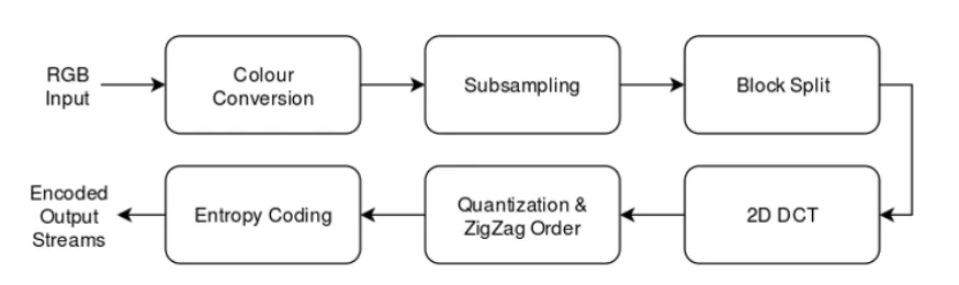
2 The JPEG Standard 4 2.1 The Encoding Process . . . 4
2.1.1 Colour Space Conversion . . . 5
2.1.2 Component Subsampling . . . 8
2.1.3 Block Splitting . . . 9
2.1.4 2-dimensional Discrete Cosine Transform . . . 9
2.1.5 Quantization and Zig Zag Order . . . 10
2.1.6 Entropy Coding . . . 11
2.2 The Decoding Process . . . 12
2.2.1 Entropy Decoding . . . 12
2.2.2 Huffman Decode . . . 13
2.2.3 YCbCr to RGB . . . 15
2.3 File Structure and Restart Markers . . . 16
2.4 Survey of JPEG Images on the Internet . . . 17
2.5 Summary . . . 18
3 Previous Research 19 3.1 Software JPEG Decompression . . . 19
3.1.1 libjpeg . . . 19
3.1.2 libjpeg-turbo . . . 20
3.1.3 NanoJPEG . . . 20
3.1.4 jpeg2000 . . . 21
3.2 Hardware JPEG Decompression . . . 21
3.3 Discrete Cosine Transform . . . 22
3.5 JPEG Codec in Hardware . . . 23
3.5.1 High Performance JPEG Decoder Based on FPGA . . . 23
3.5.2 Hardware Support of JPEG . . . 24
3.5.3 FPGA Based Baseline JPEG Decoder . . . 24
3.5.4 Hardware JPEG Decoder and Efficient Post-Processing . . . . 24
3.5.5 CUDA-Based Acceleration of the JPEG Decoder . . . 24
3.5.6 A JPEG Huffman Decoder using CAM . . . 25
3.6 Summary . . . 25
4 Proposed Solution 26 4.1 Development Board . . . 26
4.2 Communication Protocols . . . 27
4.2.1 AXI3 . . . 28
4.2.2 Control Interface . . . 29
4.2.3 Data Transfer . . . 30
4.3 Hardware Design . . . 30
4.3.1 Top Level Module - user logic.v . . . 31
4.3.2 decode.v . . . 32
4.3.3 blocker.v and header.v . . . 32
4.3.4 stream.v and huff.v . . . 32
4.3.5 idctcol.v and idctrow.v . . . 35
4.3.6 colourmap.v . . . 35
4.4 Software Interface . . . 36
4.4.1 Memory Organization . . . 36
4.4.2 Software Responsibilities . . . 37
5 Results 39
5.1 Test Structure . . . 39
5.1.1 ZedBoard Configuration . . . 40
5.1.2 Test Image Database . . . 40
5.1.3 Testing Process . . . 41
5.2 Testing for Accuracy . . . 42
5.2.1 Mean Squared Error . . . 42
5.2.2 Peak Signal to Noise Ratio . . . 42
5.2.3 Accuracy Results . . . 43
5.3 Testing for Speed . . . 44
5.3.1 Speed Results . . . 45
5.4 Hardware Reports . . . 47
5.5 Summary . . . 49
6 Summary 50 6.1 Conclusions . . . 50
6.2 Recommendations for Future Work . . . 51
References 52 A Verilog Code 54 A.1 user logic.v . . . 54
A.2 decode.v . . . 71
A.3 blocker.v . . . 78
A.4 header.v . . . 82
A.5 stream.v . . . 100
A.6 huff.v . . . 105
A.8 idctrow.v and idctcol.v . . . 127
A.9 colourmap.v and zigzagcont.v . . . 132
B C Code 137 B.1 hwjpeg.c . . . 137
B.2 hwmap.c and hwmap.h . . . 144
B.3 psnr.c . . . 146
B.4 ljpeg.c and ljpegt.c . . . 149
C Bash Scripts 159 C.1 iwhbyd.sh . . . 159
C.2 pccompanion.sh . . . 162
C.3 md5gen.sh . . . 163
2.1 An Image of Detroit . . . 6
2.2 Luminance Component of an Image of Detroit . . . 7
2.3 Chrominance Components of an Image of Detroit (Cb-Left,Cr-Right) 7 2.4 4:1:0 Subsampling Configuration . . . 8
2.5 An 8x8 block and its 2D-DCT . . . 10
2.6 Example of a Luminance Quantization Table . . . 10
2.7 Zig Zag Order . . . 11
2.8 JPEG Encoding Process . . . 12
2.9 Extended Huffman Decode . . . 14
2.10 Usenet JPEG Image Survey Results . . . 17
3.2 Block Definitions for Figure 3.1 . . . 23
4.1 AXI3 Read Burst . . . 29
4.2 Hardware Design Block Diagram . . . 31
4.3 JPEG DC Huffman Tree Example . . . 33
4.4 Huffman Table corresponding to Figure 4.3 . . . 34
4.5 Loeffler’s 8-point IDCT . . . 35
4.6 Memory Organization . . . 37
5.1 Accuracy Results . . . 44
5.2 Mobile vs. Desktop CPU . . . 46
5.3 Decode Time Results . . . 47
Introduction
Digital imaging is an extremely popular method of capturing important moments of
peoples lives. With the rapid advancements in image sensing technology, especially
on the smart phone platform, one of the problems that arises is the ability to decode
stored image data, which is very commonly stored using the JPEG codec.
1.1
The JPEG Codec
In 1992 the Joint Photographic Experts Group (JPEG) released the JPEG codec
standard under ITU-T Recommendation T.81 and in 1994 as ISO/IEC 10918-1 [1].
Their goal was to facilitate the movement of images between computers in a low
bandwidth setting by compressing the image using a multitude of techniques that
would not greatly affect image fidelity. The JPEG standard outlines the process for
encoding and decoding a JPEG image as well as four different modes of operation:
Baseline Sequential, hereinafter referred to as Baseline, encodes an image from left
to right and top to bottom in blocks. Baseline is by far the most common mode of
operation of the JPEG standard. Progressive JPEGs use multiple passes of Baseline
at increasing levels of quality, which would be ideal in a web setting where the image
can be displayed first at lowest quality, but the entire set of passes must be stored
in memory to complete the decode which vastly increases the amount of resources
required to decode a single image. Lossless and Hierarchical are so rarely used that
they will not be in the scope of this thesis.
Baseline JPEG is an inherently lossy image codec due to the processes it uses to
encode and decode image data. These processes were selected after careful
consid-eration from the JPEG group for their ability to represent multiple data well in a
compressed image, however they were not chosen for their ability to be implemented
in parallel. Decoding a JPEG is a serial process that was implemented in a time when
personal computers had only one processor and so the codec is largely designed to be
run on a single thread of execution.
1.2
Motivation of Research
In the past, people would store their photographs physically, in albums, and to view
these images they were only required to open the album. The increasing use of
smartphones has caused the decline of the physical photograph and an increase in the
number of people who carry their entire photo collection on their mobile device. Since
the invention of the smartphone, pixel counts on-screen and in onboard image sensors
have skyrocketed, with trends pointing to 8K displays with upwards of 30 megapixel
(MP) cameras. Devices today rely on software libraries and increasing CPU power to
decode these images in a timely manner. They also use thumbnails and pre-rendered
when extremely high resolution images become the norm.
The focus of this thesis is to present a System-on-Chip (SoC) module that will
alleviate the pressure on the CPU when the user wants to view their images. This
decoder module will attempt to remove the CPU from the process almost entirely
and act as a coprocessor dedicated to decoding JPEG baseline images.
1.3
Thesis Outline
Chapter 1 serves to introduce the project and motivations behind it, discussing the
current state of the market and its reliance on the JPEG standard. Chapter 2 goes
in depth on the JPEG standard, showing the encoding and decoding process and
discussing the limitations imposed on hardware by the architecture of the standard.
Chapter 3 introduces previous works that aimed to improve the performance of the
standard or the standard itself, either by hardware or software.
The proposed solution is presented in Chapter 4 and includes discussions on the
implementation and its platform, the design of the hardware, and the design of the
accompanying software. Chapter 5 presents the results produced when testing the
proposed solution for accuracy and speed, while also explaining how those tests were
performed. Chapter 6 draws conclusions from the work and gives recommendations
The JPEG Standard
The JPEG standard, while almost a quarter century old, remains the industry
stan-dard for encoded image data. This chapter serves to introduce the encoding and
decoding methods defined in the standard, and details each part of the decode
pro-cess.
2.1
The Encoding Process
The encoding process starts with a colour space conversion, subsampling by colour
component, and splitting each component into blocks depending on the subsampling
factor. The data is then put through a 2-dimensional discrete cosine transform (DCT),
it is quantized and then entropy coded. The output of this entropy coding is what
makes up the data streams that will be stored in the output file. All other necessary
information is stored in the header of the file, such as the image dimensions and the
2.1.1
Colour Space Conversion
The input image data, usually in Red-Green-Blue (RGB) format, is converted to
the YCbCr colour space, which uses one channel for luminance (Y), or brightness,
and two channels for chrominance (Cb, Cr), or colour differencing. Separating the
brightness plays an important role in the compression of the image data, as the human
eye is more sensitive to changes in brightness over a small area than it is to changes
in colour over a small area. This effect is shown in Figure 2.2, which shows the Y
channel of a selected image, and Figure 2.3 which shows the Cb and Cr channels of
that same image. Looking at these figures, there is more visual information stored in
the luminance channel than in the two chrominance channels. So typically, the two
chrominance channels are subject to greater compression throughout the different
encoding stages than the luminance channel. The first example of that is in the
Figure 2.2: Luminance Component of an Image of Detroit
2.1.2
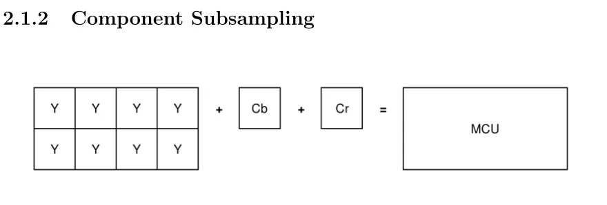
Component Subsampling
Figure 2.4: 4:1:0 Subsampling Configuration
The JPEG standard outlines an optional process to further reduce the amount of
data required to store an image while having a minimal effect on visual fidelity.
Subsampling is the process of reducing the resolution of a colour component, which
is usually only applied to the chrominance components. A Minimally Coded Unit
(MCU) is a macro block comprised of the blocks of each colour component that
represent a given region of the image. In Figure 2.4, assuming the MCU represents
the upper left corner of an image, or the starting block, and assuming each colour
component subblock is of size 8 x 8, there is much more detail in the Y component as
each value in the MCU has a corresponding Y value. The chrominance components,
however, have been subsampled to half the original vertical resolution, and
one-quarter the original horizontal resolution, so their values correspond to more than
one value in the MCU.
Subsampling is expressed as a ratio, A:B:C, where A is the horizontal reference,
B is the horizontal chrominance count, and C is the vertical chrominance count in
Figure 2.3, the subsampling is expressed as 4:1:0. The JPEG standard allows for
subsampling as long as the total number of blocks that make up an MCU does not
exceed 10, meaning there are 195 valid combinations of subsampling in the YCC
2.1.3
Block Splitting
Following the optional subsampling, the data is split into blocks, the size of which
is determined by the directional subsampling factor. The default block size is 8 x 8
and increases by a multiple of 8 for both subsampling factors which would make the
block size 32 x 16 in Figure 2.4.
2.1.4
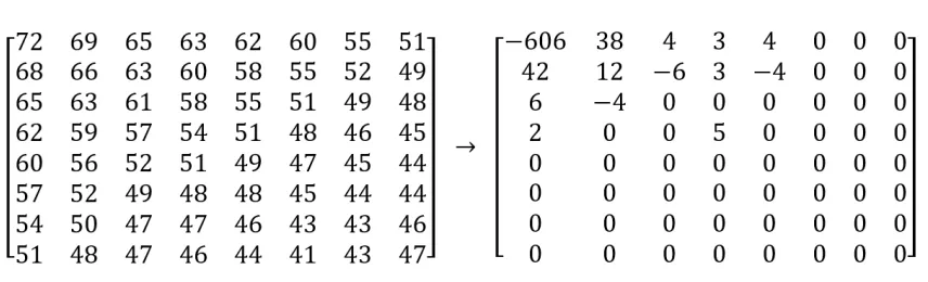
2-dimensional Discrete Cosine Transform
After block splitting, each block undergoes a 2-dimensional discrete cosine transform
(DCT) that converts the data from the spatial domain to the frequency domain. A
2D DCT is equivalent to performing a 1D DCT, shown in Equation 2.1, on each row
followed by each column.
Xk = N−1
X
n=0
xncos
kπ
N (n+ 0.5)
, k= 0 →(N −1) (2.1)
The 2D DCT is an important part of the JPEG encode process because it tends to
focus the information towards the low frequency coefficients and away from the high
frequency coefficients, which represent data that the human eye would have a very
hard time discerning. The lower frequency coefficients reside in the upper left corner
of the block, as shown in Figure 2.5, and the high frequency coefficients reside in the
lower right hand corner. The upper-left-most value after the DCT is called the DC
component, and the remaining values are called AC components, this is important as
Figure 2.5: An 8x8 block and its 2D-DCT
2.1.5
Quantization and Zig Zag Order
Quantization is another lossy part of JPEG encoding, where the elements of a block
are divided by a corresponding value in the quantization tables. These tables place
an emphasis on preserving the low frequency values of a block, while very commonly
reducing the high frequency values to zeroes. Typically, there are two quantization
tables split between the luminance and the chrominance channels.
Figure 2.6: Example of a Luminance Quantization Table
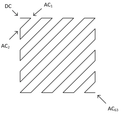
After quantization, the high concentration of non-zero coefficients in the upper left
corner of the block is taken advantage of again when the block is ordered by zigzag.
perform operations that compress the block data further than if the data was taken
in order.
Figure 2.7: Zig Zag Order
2.1.6
Entropy Coding
The final stage of encoding a JPEG is entropy coding which is comprised of Huffman
coding and Run Length Encoding (RLE) for the AC coefficients, and Huffman coding
and Differential coding for the DC coefficients. These topics are covered in Section
2.2 as they are extremely important to understanding the decoding process. The
combined outputs of theses encoders are what make up the data streams that are
stored in the body of the JPEG file. The entire encoding process is shown by block
Figure 2.8: JPEG Encoding Process
2.2
The Decoding Process
The JPEG decoding process is the reverse of the encoding process in that the data
is entropy decoded, then dequantized and put through a 2D Inverse DCT (IDCT),
the blocks of data are reassembled and undergo colour conversion from YCbCr to
RGB. The decoding process starts with gathering the necessary information from the
header of the JPEG file, such as quantization and Huffman tables, as well as image
dimensions. After the Huffman tables and quantization tables have been constructed
the decode can begin.
2.2.1
Entropy Decoding
Entropy decoding a JPEG image consists of two decoding processes: one for the DC
components using Huffman decoding and Differential decoding, and one for the AC
components using Huffman decoding and Run Length Decoding (RLD). These
pro-cesses are combined during the encoding phase, creating a hybrid encoded structure
which makes the JPEG especially taxing to decode.
match in the DC Huffman table is found. The decoded value from this match indicates
how many bits should be read next so the DC value of the first block can be obtained.
The bits are read and decoded using another table that decodes the DC value, and
this decoded value is the difference between the DC value of the previous block and
the DC value of the current block. If there is no previous block, the previous value is
assumed to be 0. With the DC coefficient being decoded, the next part of the process
is to decode the associated AC coefficients.
The bitstream is again read bit-by-bit until a match is found in the AC Huffman
table. The decoded value is 1 byte in length and has two pieces of information: the
most significant 4 bits designate how many Run-Length Encoded (RLE) zeros are to
follow the next decoded AC coefficient, and the least significant 4 bits designate how
many bits are to be read for the AC coefficient. The AC coefficient is the value of
that next number of bits and the run length zeros, a maximum of 16 of them, are the
next AC coefficients. The AC decode process is repeated until all 63 AC coefficients
have been decoded, then the next block can be decoded, again starting with the DC
coefficient.
Entropy decoding in the JPEG standard is a very expensive operation because
information is not byte-aligned in this scheme. Many blocks are contained in one scan
and there is no information on where the next block will start, so the blocks must be
decoded in order, one by one. This severely limits the options available to be able to
speed up the decode process, in hardware or software.
2.2.2
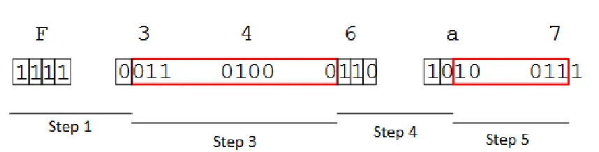
Huffman Decode
This section outlines the Huffman decode process. Particular attention should be paid
to the amount of bitwise operations that are performed on the datastream, where a
Figure 2.9: Extended Huffman Decode
1. Read datastream bit by bit, see Step 1 in Figure 2.9, until the codeword matches
a codeword found in the DC Huffman table.
Codeword: 11100
Value: 08
2. Value: 08 is the number of bits that represent the DC Huffman codeword, so
read the next 8 bits
3. Codeword: 01101000, see Step 3 in Figure 2.9, is decoded using the following
process, for DC values only
(a) Perform bitwise NOT: 01101000 becomes 10010111
(b) Decode value as unsigned integer: 10010111b = 151d
(c) Invert sign of integer: 151d becomes -151d
So the DC difference value of the first Luminance block is -151. To obtain the
DC coefficient of that block, since the element is difference encoded, we add -151
to the DC component of the previous block. In this case there is no previous
DC = 0 + (-151)
DC = -151
4. Read datastream bit by bit, see Step 4 in Figure 2.9, until the codeword matches
a codeword found in the AC Huffman table.
Codeword: 11010
Value: 05
Value: 05 is a hexadecimal byte that is formattedRRRRSSSS where:
RRRR is the number of Run Length Encoded zeros
SSSS is the number of bits to read for the next value
So for this example there are 0 RLE zeros to follow the next value, and 5 bits
will be read to obtain the 1st AC coefficient of the block.
5. Read SSSS, or 5, bits to obtain the AC coefficient, see Step 5 in Figure 2.9,
Value: 10011b = 19d
So the first AC coefficient is 19
6. Repeat steps 4 and 5 until End of Block marker is found, then repeat whole
process for the next block.
2.2.3
YCbCr to RGB
After the 2-dimensional Inverse Discrete Cosine Transform (IDCT), which is discussed
in detail in Section 3.3 and Section 4.3.5, the data has to be transformed from YCbCr
R =Y + [1.402∗(Cr−128)] (2.2)
G=Y −[0.344136∗(Cb−128)]−[0.714136∗(Cr−128)] (2.3)
B =Y + [1.772∗(Cb−128)] (2.4)
When Equations 2.2, 2.3, and 2.4 are implemented using fixed-point hardware, the
overall computational overhead for the conversion of one pixel becomes 4 additions
and 4 multiplications. This might not seem expensive, but when multiplied by the
number of pixels in an image, becomes a very taxing operation on the system.
2.3
File Structure and Restart Markers
A JPEG image file has a header-body structure, where the header contains peripheral
information, and the body contains the encoded image data. JPEGs use markers to
designate data that is relevant to certain parts of the image. The markers are 1 byte
in length and directly follow the hex byte FF to define their existence. An valid
JPEG image file will start with the Start of Image (SOI) marker, or 0xFFD8. Define
Quantization Table (DQT) or 0xFFDB, Define Huffman Table (DHT) or 0xFFC4,
and Start of Scan (SOS) or 0xFFDA are all important markers, the last of which
defines the start of the body of the image. The End of Image (EOI) marker, or
0xFFD9, ends the file.
Restart markers, or0xFFDy, are used to resynchronize an image if an error occurs.
If a restart marker is encountered, all DC differential values are reset to 0, and the
bitstream is restarted on a byte boundary following the marker. Values of y in the
restart marker encountered is 0xFFD2 and the next restart marker encountered is
0xFFD4, the decoder knows it is missing a chunk of data from the 3rd restart marker
and if enough data is present in the 4th marker, the decoder can replace the data
missing using the data in the 4th marker.
Restart markers, however uncommon they may be, present an opportunity for
multiprocessing an image decode. Using the restart markers as starting spots, an
image can be decoded by separate processes and stitched together as the processes
finish.
2.4
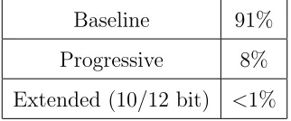
Survey of JPEG Images on the Internet
In order to get an accurate representation of how the JPEG codec is used, a survey
of available JPEG images was performed by Dr. Muscedere, provided in private
communication for this thesis. The JPEG images were found on Usenet in 2016,
where only the headers were downloaded. The survey was comprehensive, obtaining
the headers of approximately 7.35 million JPEGs, where it should be noted that
only 2 images were of JPEG2000 format. The results in Figure 2.10 show that the
overwhelming majority of JPEG images are still stored in the Baseline JPEG format.
Baseline 91%
Progressive 8%
Extended (10/12 bit) <1%
Figure 2.10: Usenet JPEG Image Survey Results
The survey also showed that about 1.2 million, or about 16% of the images used
restart intervals. So only 16% of images could benefit from a software-based
2.5
Summary
This chapter introduced the processes that make up the JPEG codec. It is important
to note the complex and serial nature of the JPEG codec, as that will govern the
development of a hardware solution. Specifically, the Huffman coding of a JPEG
limits its ability to be implemented in parallel because of the indeterminate nature
Previous Research
This chapter introduces several works that implement and improve upon the JPEG
standard. Each work has its own benefits and limitations, which are discussed in
detail to serve as a primer for the rest of the thesis.
3.1
Software JPEG Decompression
3.1.1
libjpeg
The most common way to decode a JPEG is by using the freely available libjpeg,
which is a C library that has been available since the first release of the JPEG
standard. The source code of libjpeg is a massive collection of files that implement
different functionalities based on the system for which it is being compiled to serve.
This library carries a lot of bulk with it as it tries to be a catch-all solution for every
typically not seen in JPEGs.
As of January 2016, the current release version of libjpeg is 9b [2]. It has undergone
9 major version changes since its initial release and is maintained and released by the
Independent JPEG Group (IJG).
3.1.2
libjpeg-turbo
A popular fork of the libjpeg project is libjpeg-turbo, which was built to take
advan-tage of innovations in hardware using special instructions that call upon dedicated
hardware to perform a single instruction on lots of data. Single Instruction Multiple
Data (SIMD) instructions are standard on todays microprocessors and libjpeg-turbo
uses these instructions to accelerate the processes in libjpeg. This library is
plat-form dependent because of the differences in SIMD architectures between different
companies, NEON for ARM processors and MMX/SSE2 for Intel processors. [3]
libjpeg-turbo is very common in mobile applications due to the popularity of
ARM processors in mobile phones. Because of its increase in speed, this project
will use libjpeg-turbo as a benchmark for acceleration, but not as a benchmark for
accuracy, due to its use of SIMD instructions which use reduced precision data types
for calculations.
3.1.3
NanoJPEG
Although libjpeg and libjpeg-turbo are very common, they are not well suited to
be implemented on hardware because of their numerous source files and even more
numerous configuration options. NanoJPEG is a project that attempts to implement
a JPEG decoder in a compact way, without sacrificing too much quality. NanoJPEG
is implemented in a single C file, which makes it ideal to be used as a guide for
the hardware design, as well as verification.
3.1.4
jpeg2000
In the year 2000, the JPEG group released what was supposed to be the successor
to the JPEG codec, making multiple improvements including scalable compression,
error correction, and reversible wavelet transforms instead of the traditional DCT
[5]. The issue with jpeg2000 is that patent licensing concerns have held it back,
causing the adoption of jpeg2000 to be near 0% of all images available on the internet.
Its predecessor, libjpeg, although it is 25 years old, remains the image compression
standard due to its widespread adoption and the fact that there are no licensing
concerns about the software.
3.2
Hardware JPEG Decompression
In 2013, a student at the University of Windsor, Dan Macdonald, published a thesis
called Hardware JPEG Decompression wherein he proposed a JPEG decoder that
offloaded the IDCT and colour conversion portions of the decode from libjpeg to
hardware [6]. There were improvements on the time required to decode certain images,
but there are limitations that affect the performance of the system.
The project is implemented on a Xilinx FPGA board that does not have a CPU,
which requires that the project use valuable resources to implement a soft processor
on the FPGA. Having a physical processor on board would have presented a very
substantial advantage to the acceleration of the JPEG codec, but that technology
3.3
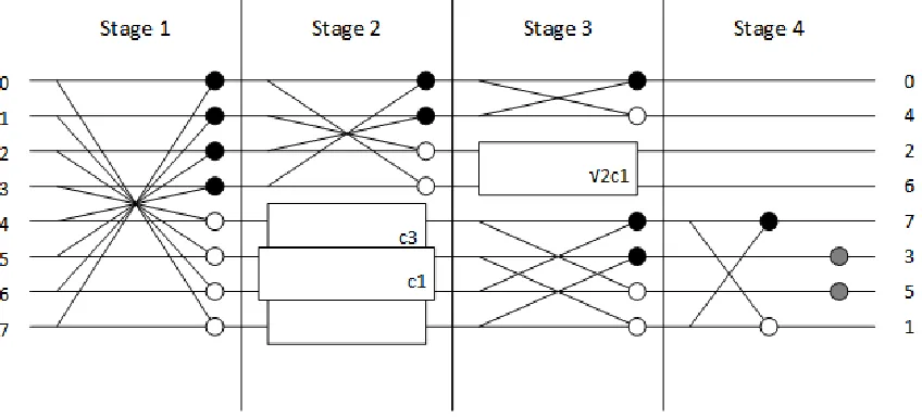
Discrete Cosine Transform
The Discrete Cosine Transform (DCT) was introduced in 1974 by Ahmed et. al as
an algorithm that could be applied to digital signal processing in the area of pattern
recognition [7]. Since the DCT and its inverse are integral to the JPEG codec, there
was a need to develop a faster version of the algorithm that could be built into
hardware or software.
In 1977, Chen et. al produced a fast DCT algorithm which was 6 times faster than
Fast Fourier Transform-based DCT implementations at the time [8]. And in 1989,
during the early development stages of the JPEG codec, Loeffler et. al introduced a
faster algorithm for computing the DCT and IDCT that only required 11 multipliers
and 29 adders for an 8-point calculation. Loeffler’s implementation took advantage of
Chen’s implementation by factoring coefficients to reduce the number of arithmetic
units required, at the expense of an increased critical path. Their designs take
ad-vantage of the even and odd symmetry of the DCT to make it a 4-stage algorithm
with significantly less hardware. [9]
Figure 3.2: Block Definitions for Figure 3.1
3.4
Fast Huffman Decoding
In 1995, Choi et. al presented a fast Huffman decoder that used high speed pattern
matching and tree clustering [10]. Their focus on reducing memory use helped video
applications at the time, but there was no mention on other performance metrics that
might be useful in the JPEG codec, such as speedup.
3.5
JPEG Codec in Hardware
3.5.1
High Performance JPEG Decoder Based on FPGA
Shan et. al presented a hardware JPEG decoder in which the Huffman decoder was
three stages that relied upon code length to calculate the memory locations of outputs.
The IDCT was a direct implementation of the Loeffler IDCT, which is the reverse
operation of that shown in Figure 3.1. Their test methodology was extremely sparse
as they only used one image for testing and they claim to be able to decode at 30
frames per second at a resolution of 1920 x 1080. Asynchronous FIFOs were used
to adjust for pipeline stalls. DDR2 and block RAMs were used as line buffer in this
3.5.2
Hardware Support of JPEG
Elbadri et. al from the University of Ottawa, in 2005, presented a survey of hardware
for the different blocks required by a JPEG encoder and decoder. Their work found
an almost 8 times speedup on a 67 MHz FPGA versus a 400 MHz CPU [12].
3.5.3
FPGA Based Baseline JPEG Decoder
In 2000, Yusof et. al proposed a baseline JPEG decoder that was able to decode at 30
frames per second for an image size of 320 x 240 [13]. Their pipeline did not include a
Loeffler IDCT but instead used the formal definition of an IDCT to create hardware,
which used a significant chunk of their available gates. Of particular interest is their
Huffman decoder which used the code length in a feedback to determine the output
of a Huffman code.
3.5.4
Hardware JPEG Decoder and Efficient Post-Processing
In 2012, Zhu and Du proposed a hardware JPEG decoder that included three
post-processing functions for embedded applications [14]. They included Inner
Down-Scaling, Region of Interest decoding, and Partial decoding, all of which would be
useful in embedded feature detection applications. Their focus was more on the
post-processing than on the inner workings of a JPEG decoder.
3.5.5
CUDA-Based Acceleration of the JPEG Decoder
In 2013, Yan et. al proposed a CUDA based JPEG decoder that was able to double
the speed at which JPEGs were decoded. They also noted that their implementation
was able to perform IDCT calculations 49 times faster than the CPU implementation,
transfer times that are significantly costly in a GPU setting [15].
3.5.6
A JPEG Huffman Decoder using CAM
In 1993, Komoto et. al proposed a high-speed and compact-size Huffman decoder
using Content Addressable Memory, or CAM [16]. Their design consisted of two
CAMs for the AC Huffman codes, each at 162 elements deep, as well as two CAMs
for the DC Huffman codes, each at 11 elements deep. The survey mentioned in Section
2.4 showed that 45.4% of JPEG images had more Huffman codes than the proposed
design had available memory locations.
The CAM is a fully custom design that is not easily scaled to different
implemen-tations. Given that 47.5% of the images in the survey use standard Huffman tables,
the CAM approach to Huffman decoding presented will not work with the majority
of today’s JPEG images.
3.6
Summary
This chapter presented previous works to be taken into consideration when building
a hardware solution for decoding JPEGs. While some solutions show promise in their
claims, they lack in their real world test results, which is where this thesis will aim
to improve upon the previous works.
There has not been much published work in developing a hardware solution for
JPEG decoding in the 25 year history of the codec, so there is either a heavy reliance
on increasing processor power by industry, or organizations are simply not publishing
Proposed Solution
This chapter serves to outline and detail the proposed solution for accelerating the
JPEG decode process. It covers the design of the SoC module as well as the board it
is implemented on, and describes the software required to control it.
4.1
Development Board
The Digilent ZedBoard was used to implement the SoC module and test its
func-tionality. The ZedBoard is a low-cost development board that features the Xilinx
Zynq-7000 SoC, as well as several other features that make it ideal for prototyping a
hardware design. The features that are of particular interest to this project include:
• ARM A9 Dual-Core CPU
• Xilinx Artix-7 FPGA
• Gigabit Ethernet
• HDMI Output
The ZedBoard having an FPGA and a CPU is a great advantage over other
development boards where the CPU must be implemented on the FPGA as a soft
processor, taking up valuable resources that could be allocated towards the hardware
design. With the CPU and FPGA being on the same chip, communication between
them is simplified and latencies are reduced, allowing for faster designs.
To facilitate the implementation of the design and its testing, a modified Linux
kernel designed for embedded systems, Linaro, will run on the ARM CPU. Linux will
be used to execute code in conjunction with the hardware, to control it and test it,
allowing for a more streamlined development environment.
This board was chosen for development because of its features, but also because it
was on the lower end of what is available to a consumer. It was certainly possible to
develop this solution on a more expensive board with better specifications, but that
would only prove this design is possible in a price range that is prohibitive to the
consumer. A goal of this project was to implement the design on a relatively
inex-pensive board, thereby increasing the accessibility of the market, without handcuffing
the development process by selecting a board without enough features.
4.2
Communication Protocols
The Zynq-7000 All-Programmable SoC contains a CPU and an FPGA that need to
communicate to complete tasks in unison. The ARM CPU dictates the use of an
open source communication protocol called AXI which is a specification of the open
source ARM Advanced Microcontroller Bus Architecture (AMBA). AMBA Advanced
3 and 4, where IP Cores defined by the specification and custom AXI solutions are
part of the design.
4.2.1
AXI3
The target device uses AXI3 as its communication protocol. The Xilinx software
provides the option to use AXI4, but upon further investigation, if a design uses
AXI4, the software inserts AXI bridges to convert the AXI4 transfer to AXI3, which
adds unnecessary bulk to the FPGA design.
AXI3 is a burst-based handshake protocol that uses two-way VALID and READY
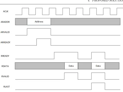
signals. It allows up to 16 transfers per burst, and transfer sizes up to 1024 bits. In
Figure 4.1, an example of an AXI3 read burst is shown. The master asserts ARVALID
and places the address on the ARADDR bus, the slave asserts ARREADY and takes
reads the address from the bus. After deasserting ARVALID, the master asserts
RREADY to signal it is ready to take in data. The slave places the data on the bus
and asserts RVALID. The master and slave know a transaction is complete when both
RREADY and RVALID are asserted simultaneously on a rising clock edge. On the
Figure 4.1: AXI3 Read Burst
4.2.2
Control Interface
Controlling the SoC module is paramount to its operation, whether the commands
are simple or a kernel driver is implemented, the fundamentals of communication are
the same. AXI4-lite defines a set of software accessible hardware registers that have
a relatively low bandwidth compared to its siblings, AXI4 and AXI4-stream. These
registers are used in the SoC module to convey control information and receive status
information.
The control registers are assigned a memory address when the kernel is booted,
this address is hardcoded in the Linux systems device tree, which is a file that is
assigned to the address of the hardware registers, so they can be read from or written
to by referencing the pointer.
4.2.3
Data Transfer
After the control registers have been set and the command to begin the decode is
given, the image is pulled from a predetermined location in DDR3 RAM in chunks of
a preset size. The SoC Module does all of this, there is no interference from software
after the control registers have been set. The transfer happens over AXI3, with a
burst size of 16 words per transfer.
The Zynq processor on the ZedBoard natively uses all AXI3. AXI4-lite is AXI3
with 1-word transfers so it is easier to implement. AXI4 is simply AXI3 but with
transfers extended from 16 word to 256 words. The IP block is imported into Xilinx
Platform Studio and it automatically creates a bridge from AXI3 to AXI4-lite for the
command channel, whereas the main memory transfer does not require a bridge.
AXI is a master-slave bus protocol and the proposed solution takes advantage of
this by being a master for memory transfers, and a slave for control registers. This
allows the SoC module to be independent of the CPU when reading or writing data
to and from RAM. Not having to wait for the CPU to push and pull new data is an
enormous advantage over other solutions currently available.
4.3
Hardware Design
The hardware design is comprised of many submodules that separate the functionality
of the JPEG codec into a sort of pipeline. Figure 4.1 shows the overall design pipeline,
this subchapter will serve to thoroughly explain each submodule in the order that the
Figure 4.2: Hardware Design Block Diagram
4.3.1
Top Level Module - user logic.v
The top level module, user logic.v, is responsible for implementing the software
ac-cessible registers for control of the system, interfacing with RAM to read and write
(FIFO) buffers. This module acts as the go-between for software and hardware.
4.3.2
decode.v
The next module the data encounters is the decode module which is responsible for
the flow of data into and out of the system at a rate that the other submodules
can handle it. It creates the instances of all the other submodules and facilitates
communication between them so as not to overload the system with data. Each
submodule can report to the decode module whether they have too much data or not
enough data, allowing the decode module to stall the pipeline or the input data until
the system has caught up. This submodule also implements the ability to change the
size of the input data based on the subsampling rates, and is responsible for making
sure the output data is aligned when it is written.
4.3.3
blocker.v and header.v
The blocker module takes data from the input FIFO and splits it into 8-bit chunks so
that the next module, the header module, can take those bytes and parse the header
information. The header module reads this data and passes important information
such as Huffman tables, Quantization tables, and image properties to the decode
module. This information will be used throughout the rest of the image decode and
is extremely important to the functionality of the SoC module.
4.3.4
stream.v and huff.v
The stream module takes the output of the header module and is designed to feed that
data, bit by bit, to the huff module, which is responsible for the Huffman decoding
of the data. Since the JPEG codec only allows Huffman lengths of up to 16 bits,
left-most value at that depth of the tree as an offset to quickly determine Huffman
decoded values. Figure 4.3 shows an example of a tree, where storing the left-most
elements at each level in a lookup table can greatly reduce the amount of hardware
needed to lookup a value in the Huffman Table.
Figure 4.3: JPEG DC Huffman Tree Example
The Huffman module keeps track of the number of codes at each depth, as well
as the code and the bit representation for that code. The hardware performs all 16
subtractions on the input in question and looks for positive result from the lowest
level on the tree (or the highest bit length), which indicates that the code being
searched for is on that level of the tree.
bit-lengths 5-16 would result in overflow. The lookup table containing the codes are in
order, allowing the code to be extracted by knowing the position of the code for the
first 4-bit word, plus an offset. In this case, 5 + (1110b - 1100b) = 7, so the 7th
element is extracted from the lookup table.
Length Bits Code (Hex)
2 bits 00 05
01 06
3 bits
100 04
101 07
4 bits
1100 01
1101 02
1110 03
5 bits 11110 08
6 bits 111110 00
7 bits 1111110 09
Figure 4.4: Huffman Table corresponding to Figure 4.3
Another feature of the Huffman module is that it uses a predictor to indicate to
the Stream module, which is feeding it data, how many bits should be skipped to
start obtaining the next Huffman word. This is accomplished by feeding the length
of the payload back to the Stream module and having it skip that number of bits.
Allowing the Stream module to shift before the current operation is done allows the
system to save 1 cycle per Huffman decode by having the next codeword ready before
it is needed.
There are three concurrent processes in the Huff and Stream modules, one to
and the third to store it in a buffer for that block. The predictor helps by maximizing
the parallelism of the two modules, allowing the Stream module to have the next
Huffman code ready for decode in most cases.
4.3.5
idctcol.v and idctrow.v
The two IDCT modules are responsible for performing the 2D IDCT separated into a
row operation followed by a column operation. Loefflers IDCT is the implementation
used in these two modules, each taking 14 cycles from final input to final output.
The two modules are both split into separate stages because the system cannot feed
enough data to the 2D IDCT for it to be implemented in a single cycle.
Figure 4.5: Loeffler’s 8-point IDCT
4.3.6
colourmap.v
Following the 2D IDCT, the colourmap module takes the decoded data and converts
output because it matches the framebuffer format for the ZedBoard, allowing for the
decoded images to be displayed on an HDMI connected monitor.
4.4
Software Interface
A fully customized software interface was designed in C to interact with the hardware
via its software accessible registers. The software has no role in the actual JPEG
decode, and is present only to control and check the status of the hardware.
4.4.1
Memory Organization
The ZedBoard contains 512 MB of DDR3 RAM, of which most is used by the Linux
kernel as main memory. By passing an argument to the kernel as it is booting, a
portion of this memory is reserved and the kernel does not allocate it. This shared area
of memory can be used to communicate large chunks of data between the hardware
and the software. The shared memory area is split into two buffers, a read buffer and
a write buffer, and because of the compressed nature of the JPEG, the write buffer is
many times the size of its counterpart. Figure 4.6 shows how memory was allocated
Figure 4.6: Memory Organization
4.4.2
Software Responsibilities
The software starts by resetting the hardware so it is in a deterministic state. The
read buffer in shared memory is then set to an arbitrary size. The size of the read
buffer should be realistic and based on the amount of available memory and the size
of the image. The image file is then opened so that the read buffer can be filled. The
first read is important because it fills control registers with important values such
as image size and subsampling factor, as well as allowing the Huffman tables and
Quantization tables to be decoded by hardware.
During the initial read, the size of the write job is set to zero so that no information
important information from the hardware that is used to determine the size of the
write buffer and subsequent write jobs. Without doing this, the software would have
no information on the size of the image and would not be able to control file writing
to properly output the image.
Now that the software can properly set a write size, the program enters its main
loop, in which it polls the software for completion of either a write job or a read job
and starts the next corresponding job. Upon a write job finish, the information is
read from memory and written to file, and upon read job completion, the next block
of information is read from the JPEG file and written to the read buffer. When an
image decode is finished, a bit is set in the status register and the software is designed
to clean up and exit its execution.
4.5
Summary
Presented in this chapter was a fully custom hardware solution for decoding JPEG
images. The next chapter will introduce the methods used to test the SoC Module’s
performance in two aspects, speed and accuracy, as well as present the results of these
Results
This chapter presents results that were generated during the testing of the proposed
Custom SoC Module. It also describes the methodology used to test the solution for
accuracy and speed.
5.1
Test Structure
The goals of testing the module were to determine its characteristics such as speed and
accuracy, while removing delays associated with I/O to obtain accurate test results.
Removing I/O associated delays from the measurements was important because of
the massive difference between the configuration of the ZedBoard, which uses a
Net-work File System, and a smartphone, which uses high performance flash memory.
In addition to this, the benchmark would far outperform the module if the images
converted by the desktop workstation were stored on a SATA drive and the ZedBoard
the different factors associated with testing two vastly different systems.
5.1.1
ZedBoard Configuration
The Linux kernel on the ZedBoard has a multitude of customization options, one
of which is the ability to have the root filesystem, on which the Linux system is
stored, be on a Network Filesystem (NFS). This option was a great opportunity to
have the workstation filesystem double as the ZedBoard filesystem, greatly reducing
the differences between the two test environments. The increased overhead of the
NFS root filesystem running over Gigabit Ethernet (GbE) pales in comparison to
the increase in filesystem speed and responsiveness over the SD Card interface at 10
MB/s.
The ZedBoard relies on a binary file to do a few things during its boot sequence
and this file is stored on the SD Card. The boot binary is responsible for programming
the FPGA portion of the board, as well as pointing the First Stage Bootloader (FSBL)
to the kernel executable and the device tree file, which tells the kernel the types of
hardware that are available to it and their respective addresses. When the kernel
takes over the boot process, it continues with a standard Linux boot that presents
the user with a command line interface. The user can then develop software that can
operate in conjunction with the FPGA, without having to reboot the board every
time a change in software is made. This creates a very user friendly development
environment in hardware prototyping.
5.1.2
Test Image Database
The images used to test the SoC Module were obtained by scraping Flickr, a popular
image hosting website, for images that were license-free and taken from an iPhone
and allows for the images to be made available upon release of this thesis. The image
database totals 8760 images, giving a fairly good overall coverage of what the average
users image might be.
5.1.3
Testing Process
The testing process is made up of several sub-processes that were optimized to be as
efficient as possible with the hardware available. These processes are split between
running on the ZedBoard when necessary, and the workstation, which is a much more
powerful machine. Because the workstation and the ZedBoard share a filesystem,
file-based multiprocessing was implemented using BASH scripting on both machines.
The process starts with the workstation decoding a JPEG into what is referred to
as the golden image. This golden image is the result of the libjpeg decoder running
with the float option for IDCT, it will be used as a benchmark for comparison later in
the testing process. In order to save storage space on the shared filesystem, a hashing
algorithm, MD5, is used to create a signature of the decoded image and will be used
to compare the results of ZedBoard running the exact same configuration of libjpeg
only.
The ZedBoard decodes the image, performs the MD5 hash, and compares it to
the workstation generated MD5. This is a sanity check as the MD5 hashes should
always match between the ZedBoard and the workstation because the code bases
are the same. The ZedBoard is then responsible for creating six additional outputs
for comparison to the golden image. At the end of output generation for one input
image, outputs exist for libjpeg with three switches (float, fast, and slow),
libjpeg-turbo (float, fast, and slow), and a SoC Module output.
The following sub chapters will describe in detail the methodologies used to
and introduce results for both.
5.2
Testing for Accuracy
In order to test for accuracy between the golden image and the different decoders,
a need exists for a way to measure the differences between two images that, to the
naked eye, may look exactly the same. A simple eye test might work for images
with significant differences in pixel values, but a more concrete method will provide
a better understanding of the differences between different decoding methods.
5.2.1
Mean Squared Error
It is possible to use Mean Squared Error (MSE) to create values that represent the
differences between the golden image and the output of the decoders. The MSE
of a grayscale image is shown in the equation below. This formula is useful for
grayscale images, but when the input is an RGB or CMYK image, the increase in
colour components will artificially increase the output value of the MSE function.
Normalizing this function according to the quantity of colour channels would eliminate
bias associated to increasing numbers of colour channels, which is where Peak Signal
to Noise Ratio becomes useful.
M SE= 1 mn
m−1
X
i=0
n−1
X
j=0
[I(i, j)−K(i, j)]2 (5.1)
5.2.2
Peak Signal to Noise Ratio
Peak Signal to Noise Ratio (PSNR) is a common way to measure the power of a
signal, which in this case would be the output image from the set of decoders. PSNR
MSE. This allows for different colour schemes to be measured easily by adjusting the
max value, shown in Equation 5.2.
P SN R= 20∗log10(M AXI)−10∗log10(M SE) (5.2)
where
M AXI = 2B−1 (5.3)
where B is defined as the number of bits per sample
5.2.3
Accuracy Results
Using libjpeg-turbo as a benchmark, because of its widespread use in mobile
appli-cation development, the hardware image output is measured using PSNR. PSNR is a
measure of signal power, which means that if two images match exactly, the output of
the function will be infinity, which is not able to be shown on a graph, so the output
was modified from infinity to a value of 300dB.
A moderate grouping of ”perfect” decodes by libjpeg-turbo with the float option
for DCT can be seen at the top of the chart, as well as a grouping of images that
were more accurate than hardware around the 200dB mark in Figure 5.1. But for the
majority of images, the hardware was able to outperform the software because the
software rounds values after every stage, whereas the hardware was built to round
Figure 5.1: Accuracy Results
5.3
Testing for Speed
An important metric in hardware acceleration is the speedup that results on a given
process. It is important to know what to measure and how to measure it so there are
no false positives in the measurement process. This was difficult to ascertain for this
project because of the hardware focused nature of the SoC Module. Measuring the
hardware in clock cycles and the software in time, the most accurate way to make
a comparison is to eliminate as many of the variables surrounding the two tests as
possible.
When measuring the time software spent decoding a certain image, the
for the separation of user time and system time, where user time is the time spent
actually running the software, excluding system events such as disk reads and writes.
Removing system events from the measurement allowed for the direct comparison
of user time to the number of clock cycles that hardware spent decoding that same
image. On top of getrusage, a switch was implemented in the software to disable disk
writes entirely so a speed run of each of the seven decoders could be done during
processing.
The clock cycles are measured by hardware counters that are software accessible.
Three measures of clock cycles occur: one when only the read portion of the hardware
is active, one when only the write portion of the hardware is active, and one when
both portions are active. Summing these three counters gives an accurate account of
how much work was done because it discounts periods of time when neither system
is active due to data stalls from software.
5.3.1
Speed Results
To present an argument that mobile CPUs have not yet caught up to Desktop CPUs,
a comparison was done using libjpeg-turbo (float) of decode times on the ZedBoard
and a workstation. The workstation is a mid-level machine from 2010 that features an
Intel Xeon E5450 4-core CPU at a clock speed of 3.0GHz, and 8 GB of ECC DDR3.
Figure 5.2 shows that the older workstation CPU far outperforms the mobile ARM
Figure 5.2: Mobile vs. Desktop CPU
Again using libjpeg-turbo as a benchmark, decode times were compared. There is
a large grouping, in Figure 5.3, where decode times for images under 10 megapixels are
similar, but hardware still shows an improvement over software. Where the greatest
improvement is seen is for images over 10 MB and especially on those over 15 MB. On
average, hardware was 5.57 times faster than libjpeg-turbo with float DCT, and 4.14
times faster than libjpeg-turbo with fast DCT. Combine the speed increases with the
results shown in Section 5.2, and the SoC Module vastly outperforms software even
Figure 5.3: Decode Time Results
To summarize the performance of the system, the average pixel processing speed
was found to be 0.494 pixels/cycle, and the Huffman payload processing speed was
2.259 cycles/payload.
5.4
Hardware Reports
The overall design of the SoC Module uses roughly 18% of the available resources
on the FPGA, as seen in Figure 5.4. This is possible because there is no need to
implement a soft processor on the FPGA. Figure 5.4 shows the design was easily able
Number of RAMB18E1s 7 out of 280 2%
Number of RAMB36E1s 1 out of 140 1%
Number of Slices 2525 out of 13300 18%
Number of Slice Registers 3508 out of 106400 3%
Number of Slice LUTS 6917 out of 53200 13%
Number of Slice LUT-FF pairs 7386 out of 53200 13%
Figure 5.4: Resource Usage on the FPGA
There were limitations caused by the software used to develop the solution. The
CPU/FPGA design could not be simulated because of the number of pins required
to simulate a physical CPU, which caused significant delays in the design process.
Physical debugging is extremely difficult compared to simulation debugging, but it
was necessary because of the design of the ZedBoard.
Xilinx’s software has its limitations as well, providing vague information on the
critical path of the design. This made it difficult to make incremental improvements
on the design. The critical path was found between the Stream module and the Huff
module, which was expected due to the bit-by-bit nature of the JPEG data stream.
Although the FPGA software validated a successful implementation at 66MHz, in
practice it was unstable. The next lowest option of 50MHz was used for all testing.
An option to combat all of these issues was to use a more expensive development
kit, but the goal of the project was to implement it on hardware that was inexpensive.
This was in an effort to show that consumer accessible hardware could run the design
5.5
Summary
It was shown in this chapter that full hardware acceleration of JPEG decoding has
clear and distinct advantages over its software counterparts. A 5x speedup on FPGA
combined with the increased accuracy for greater visual fidelity, if this SoC Module
were to be implemented as an ASIC and put alongside a CPU as a coprocessor, it
Summary
6.1
Conclusions
The popularity of the JPEG codec makes it an excellent candidate for hardware
acceleration. Furthering this candidacy is the rapid advancements in image sensor
technology and smartphone display technology. Licensing issues have dictated the
software market for many years, causing the image codec monopoly that is currently
held by the JPEG. A need for faster image decompression exists where the vast
majority of images rely on a 25-year-old codec that was not built with multiprocessing
in mind.
This work presented an all-encompassing solution for JPEG decoding using FPGA
hardware. The benefits of hardware acceleration are clear, with the proposed solution
outperforming software solutions at a fraction of the clock rate. The added benefit
hetero-geneous system to perform other tasks, providing a better overall user experience.
The architecture presented in this work is entirely novel at the time of writing.
No other publicly available solution presents a hardware module that can decode a
JPEG in its entirety, only relying on the CPU for memory transfers.
Taking into account the large number of IP cores being built into modern SoC
designs, this module is small enough to be added to those designs with a minimal
increase in size and cost, as shown in Figure 5.4.
Additionally, a full ASIC implementation would improve the speed of the circuit,
with Kuon and Rose [17] showing that ASIC implementations provide speedups of
about 4x against FPGA implementations of the same circuit in a 90nm process.
6.2
Recommendations for Future Work
The implementation presented in this work substantially improves the process of
decoding a JPEG, however it is not a market ready solution. A Linux kernel driver,
if properly designed and implemented, would greatly improve performance and allow
for a more seamless experience on the side of the end-user. Proper context switching
in the driver would allow for multiple images to be decoded at the same time. Two or
more processes could submit decode jobs that would be switched based on time-slice
[1] G. K. Wallace, The JPEG still picture compression standard, IEEE Trans. Con-sum. Electron., vol. 38, no. 1, pp. xviii–xxxiv, 1992.
[2] Independent JPEG Group, Independent JPEG Group. [Online]. Available: http://ijg.org/. [Accessed: Feb-2015].
[3] libjpeg-turbo, libjpeg-turbo — Main / libjpeg-turbo. [Online]. Available: http://libjpeg-turbo.virtualgl.org/. [Accessed: Feb-2015].
[4] NanoJPEG: a compact JPEG decoder, KeyJs Blog RSS. [Online]. Available: http://keyj.emphy.de/nanojpeg/. [Accessed: Feb-2015].
[5] A. Skodras, C. Christopoulos, and T. Ebrahimi, The JPEG 2000 Still Image,
IEEE Signal Process. Mag., vol. 18, no. September, pp. 36-58, 2001.
[6] D. Macdonald, Hardware JPEG Decompression, 2013, University of Windsor.
Electronic Theses and Dissertations. Paper 4889.
[8] W.-H. Chen, C. Smith, and S. Fralick, A Fast Computational Algorithm for the Discrete Cosine Transform, Commun. IEEE Trans., vol. 25, no. 9, pp. 10041009, 1977.
[9] C. Loeffler, a. Ligtenberg, and G. S. Moschytz, Practical fast 1-D DCT algorithms with 11 multiplications,Int. Conf. Acoust. Speech, Signal Process., pp. 2-5, 1989.
[10] S. B. Choi and M. H. Lee, High speed pattern matching for a fast huffman decoder, IEEE Trans. Consum. Electron., vol. 41, no. 1, pp. 97-103, 1995.
[11] J. Shan, D. Wang, and E. Yang, High performance JPEG decoder based on FPGA, Asia Pacific Conf. Postgrad. Res. Microelectron. Electron., pp. 57-60, 2011.
[12] M. Elbadri, R. Peterkin, V. Groza, D. Ionescu, and A. El Saddik, Hardware support of JPEG, Can. Conf. Electr. Comput. Eng., vol. 2005, no. May, pp. 812-815, 2005.
[13] Z. M. Yusof, Z. Aspar, and I. Suleiman, Field programmable gate array (FPGA) based baseline JPEG decoder, 2000 TENCON Proceedings. Intell. Syst. Technol. New Millenn. (Cat. No.00CH37119), vol. 2, pp. 218-220.
[14] K. Zhu, W. D. Liu, and J. Du, Hardware JPEG Decoder and Efficient Post-Processing Functions for Embedded Application,2012 IEEE 12th Int. Conf. Com-put. Inf. Technol., pp. 814-817, 2012.
[15] K. Yan, J. Shan, and E. Yang, CUDA-based acceleration of the JPEG decoder,
Proc. - Int. Conf. Nat. Comput., pp. 1319-1323, 2013.
[16] Komoto, E., Homma, T., and Nakamura, T., A High-speed and Compact-Size JPEG Huffman Decoder using CAM, Symposium 1993 on VLSI Circuits, pp. 3738, 1993.
Verilog Code
A.1
user logic.v
module user logic (
S AXI RVALID, S AXI RREADY, m axi aclk, m axi aresetn, m axi arready, m axi arvalid , m axi araddr, m axi arlen, m axi arsize , m axi arburst, m axi arprot, m axi arcache, m axi rready, m axi rvalid , m axi rdata, m axi rresp, m axi rlast , m axi awready, m axi awvalid, m axi awaddr, m axi awlen, m axi awsize, m axi awburst, m axi awprot, m axi awcache, m axi wready, m axi wvalid, m axi wdata, m axi wstrb, m axi wlast, m axi bready, m axi bvalid, m axi bresp ) ; // user logic
input S AXI ACLK;
input S AXI ARESETN;
input [31:0] S AXI AWADDR;
input S AXI AWVALID;
output S AXI AWREADY;
input [31:0] S AXI WDATA;
input [3:0] S AXI WSTRB;
input S AXI WVALID;
output S AXI WREADY;