Abstract
YUCE, MEHMET RASIT. A Differential-Based Multiple Bit Rate PSK Receiver: Theory, Architecture, and SOI CMOS Implementation.(Under the direction of Professor Wentai Liu.)
The development of telecommunications electronics with low power and low mass will be significant for future deep-space communications. The design of a receiver for deep-space communication requires the receiver to be robust against frequency variations due to Doppler effect in addition to radiation tolerance and low-power consumption. This dissertation reports a very low-power differential-based phase-shift keying (PSK) receiver that is targeted at deep space and satellite communications, on both architectural and implementation levels. The power consumption of the PSK baseband circuit alone is less than 100 µW, which is significantly better than previously reported designs. Another major feature that has not been previously offered for PSK modulation is the use of 1-bit analog-to-digital converter (ADC) with sub-sampling front-end.
The receiver uses double differential detection with traditional PSK modulation in the baseband to eliminate the impact of Doppler shift. Furthermore, the baseband can be employed in IF-sampling and sub-sampling front-end. Both front-ends offer minimal power consumption and differ from many traditional ones by eliminating some existing problems such as DC offset, dc voltage drifts and 1/f noise. The receiver also incorporates digital decimation stages to accommodate variable bit rates, and therefore it is highly programmable. The ability to support a wide range of data rates is an important feature of the receiver. This is achieved via digital channel selection by means of digital signal processing (DSP). A timing circuit robust to Doppler shift is also introduced for the proposed PSK receiver. Unlike conventional timing circuits, the proposed circuit consists of a 1-bit ADC at the front to convert analog signal to digital signal and a pre-filter to eliminate frequency error due to Doppler. In addition, the circuit is designed for multiple bit rates. The worst-case observed timing offset from the implementation for all data rates is less than 1/10 of the symbol period of the highest bit rate 100 Kbps (i.e. ∆TBmax B=1 µs).
currently the most attractive choice in transceiver designs due to its advantages in both speed and power over standard CMOS because of lower parasitic capacitances. The designed baseband circuit consumes a power as low as 90.6 µW from a 1.1 V power supply. The analog part of the designed test chip consists of a two-stage differential IF amplifier that consumes a power of 0.8 mW from a 2.5 V supply. The primary goal of the proposed receiver is to achieve a higher integration at chip level, therefore resulting in significant size, power, and mass reductions for orbiter-lander communications while still meeting the system-level constraints.
This dissertation also identifies the implementation issues of wideband next generation receivers. The recent trend for IC designers is to design extremely flexible receivers that can support multiple standards in wireless communication. Thus the aim of the next generation receivers is to operate with multi-standard and multi-band channels. Herein, new sampling wideband front-end architectures are discussed for this application. The proposed architectures are well suited for wideband receiver architectures due to the limited dynamic range of analog-to-digital converters (ADC’s) in today’s technology. They differ from conventional types by providing low power and high integration.
A DIFFERENTIAL-BASED MULTIPLE BIT RATE PSK RECEIVER: THEORY, ARCHITECTURE, AND SOI CMOS IMPLEMENTATION
by
MEHMET RASIT YUCE
A dissertation submitted to Graduate Faculty of North Carolina State University
in partial fulfillment of the requirements for the Degree of
Doctor of Philosophy
ELECTRICAL AND COMPUTER ENGINEERING
Raleigh, NC 2004
APPROVED BY :
Biography
Acknowledgement
The materials presented in this dissertation are results of many discussions with some individuals whom I have worked and discussed with during my graduate study. First of all, I have definitely been blessed by working under one of the most encouraging advisors, Dr. Wentai Liu. I would like to express my gratitude to him for his support and his guidance during my graduate studies. I would also like to express my sincere appreciation for Dr. Ralph Cavin, Dr. Gianluca Lazzi, Dr. Numan Dogan, Dr. Sandra O. Paur, and Dr. Fuh-Gwo Yuan for serving on Ph.D. my committee. Very big thanks go to Dr. Paul Franzon. I am grateful for his help through NASA’s project and his useful discussions and guidance.
I would like to thank to former and present members of my research group at North Carolina State University as well as at University of California at Santa Cruz: Mustafa Dagtekin, Rizwan Bashirullah, Alper Kendir, Kassin Vichienchom, Jeff Marks, Liang Zhang Praveen Singh, Guoxing Wang, and Mohanasankar Sivaprakasam. I like to express my appreciation for Ranjeet Jhutti, Mark Oehlberg, and Jerrel Rensch for reading some part of my dissertation. To John Damiano and Bhaskar Bharath, thanks for many discussions during our project meetings. I have had great and useful time with them. Special thanks go to Dr. Dogan’s research group at NC A&T University as well; Ertan Zencir, Douglas and Ahmet Tekin. Also, thanks to Steve Lipa for the help in the laboratory facilities during measurements.
And finally, I wish to thank my parents for their support, encouragement and understanding. Without their love and dedication I would not have made it so far.
Table of Contents
List of Figures……… VIII
List of Tables………... XIII
Organization of Thesis ………XIV
Chapter I ……… 1
Introduction………... 1
1.1. Motivation………... 1
1.2. References………... 3
Chapter II ………... 4
Low Power CMOS Wireless Communications: System and Circuit
Design Analysis………... 4
2.1. Introduction ………4
2.2. Traditional Receiver Architectures………. 5
2.2.1. Heterodyne Receivers……… 5
2.2.2 Direct Conversion Receivers………. 7
2.2.3. Low-IF Receivers………...10
2.2.3. A. Image Rejection in Low-IF and Wide Band IF………. 12
2.2.4. Digital IF Receivers………... 13
2.3. Next-Generation Receiver Architectures………... 14
2.3.1. Software-Defined Radio (SDR) Receivers………... 17
2.3.2. Ultra-Wide Band (UWB) Receivers……… 17
2.3.3. MIMO Receiver Architectures……… 19
2.4.
Alternative Front-end Architectures for Wideband Multi-standard
Receivers ………. 21
2.4.2. (Sub)-sampling Receiver Architectures………... 23
2.4.3. IF (Sub)-sampling Receiver Architectures………...25
2.5. Key Parameters in Designing Low-power and High Performance
Transceivers………. 29
2.6. Ultra Low-Power PSK Receiver Architectures………... 34
2.7. Conclusion ………... 38
2.8. References……… 40
Chapter III ………... 44
Silicon on Insulator (SOI) CMOS Technology: its Applications in
Transceiver Design ……….. 44
3.1.
Introduction ……….44
3.2.
SOI CMOS Devices………. 45
3.3.
Partially-Depleted SOI Layout Density………49
3.4.
SOI CMOS in Analog-Digital RF Mixed Circuits………... 51
3.5.
Conclusion……… 53
3.6.
References……… 54
Chapter IV ………... 55
A Low Power PSK Receiver for Space Applications in 0.35 µm
SOI CMOS ………... 55
4.1.
Introduction ………. 55
4.2.
Space Communications ………... 57
4.2.1. Doppler Analysis ……….57
4.2.3. A Modulation Scheme Robust to Doppler………... 63
4.3.
A Differential-Based Sampling PSK Receiver for Space
Applications………... 64
4.3.1. System Description……….. 64
4.3.1. A.Receiver Front-ends………... 69
1-) 1-bit ADC Front-end…………… 69
2-) Subsampling Front-end……… 70
4.3.1. B. DDPSK Signal Model and BER Performance………. 74
1-) Auto Correlated Signal Model in 1-bit ADC Front-End…………………..74
4.4. Overall Receiver Performance………...………78
4.4.1. Quantization Error………78
4.4.2. Synchronization………80
A. Symbol Timing Recovery (STR)………... 80
B. Symbol Timing Error………. 82
C. Error in Delay Units………. 82
4.5. Conclusion……… 87
4.6. References……… 88
Chapter V ………. 90
Synchronization for PSK Receivers: A Low-Power All-Digital Symbol
Timing Recovery Circuit for Multi-Bit Rate PSK Receivers ……….. 90
5.1.
Introduction ………. 90
5.2.
All-Digital Symbol Timing Recovery Circuit (STR)……….. 92
5.3.
Some Simulation Results ……… 99
5.4. Conclusion……….. 103
Chapter VI……….. 105
VLSI Implementation and Test Results………... 105
6.1.
Introduction ………... 105
6.2.
1-bit ADC Front-end (Analog Part)………... 107
6.3.
Multirate Transmission………...109
6.4.
Experimental Results………..111
6.5.
Measured Power Consumption………...120
6.6.
Conclusion……….. 122
6.7.
References……….. 123
Chapter VII……….124
Conclusions………. 124
7.1.
Summary of Contributions………. 124
List of Figures
Figure 1.1. Next generation receiver architecture …………...………. 1
Figure 2.1. Heterodyne receiver architecture………..………..6
Figure 2.2. Frequency plan of a heterodyne receiver………...……….6
Figure 2.3. General schematic of direct conversion receiver a) simple direct-conversion receiver b) I/Q down conversion direct conversion receiver………. 8
Figure 2.4. Self-mixing of LO signal and a strong interferer………8
Figure 2.5. A PSD of the down converted signal with impairment effects in down-con-version receivers……… 9
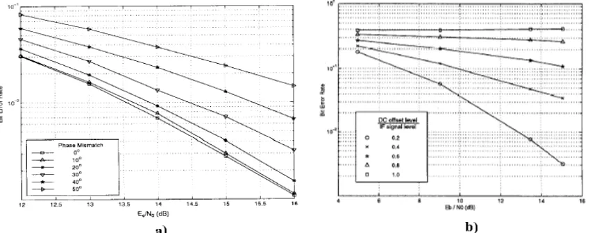
Figure 2.6. Impairment effects in 4-FSK down-conversion receiver, a) degradation due to I/Q phase mismatch [11] b) the effect of DC offset on the BER performance [12]……….. 10
Figure 2.7. A low-IF receiver………..11
Figure 2.8. A wideband double-conversion IF receiver…….………12
Figure 2.9. Mixing with a complex exponential………12
Figure 2.10. The spectrums of the inputs and outputs of down conversion mixers a) the mixing of a real signal with an exponential signal b) the mixing of a complex signal with an exponential signal………... 13
Figure 2.11. Power efficiency of ADC’s [31]………...16
Figure 2.12. ADC power dissipation versus resolution [32]………...…..16
Figure 2.13. An ideal SDR configuration………..17
Figure 2.14. Waveforms and spectrums of conventional communication systems and UWB systems [38][36]………... 18
Figure 2.15. UWB transceiver architecture [38]……….………..18
Figure 2.16. Different modulation techniques for UWB pulses, a) OOK, b) PAM, c) BPSK, and c) PPM………...19
Figure 2.17. MIMO communication architecture……….………20
Figure 2.18. Channel capacity of MIMO vs single conventional receiver [42]………20
Figure 2.19. Sampling: (a) Nyquist sampling for a lowpass signal, (b) bandpass sampling (subsampling)………... 21
Figure 2.21. An IF (sub)-sampling receiver architecture……….25
Figure 2.22. A subsampling architecture for wide-band digital receivers a) a multi-standard radio architecture b) digital down conversion (DDC) at each stage………. 26
Figure 2.23. Cascaded decimation filter structure for multirate in wideband digital radio. The channel-select processing is done digitally in a wide-band subsampling receiver………... 26
Figure 2.24. An IF (sub)sampling multi-standard receiver architecture………..……27
Figure 2.25. A Comb filter implementation as a decimation filter………..……….28
Figure 2.26. Frequency response of Comb filters, a) cascaded Comb filter for different decimation rates, b) Frequency responses of 4, 6 and 8-order Comb filters (fs =128 MHz)………. 29
Figure 2.27. Waveforms for several modulation schemes: ASK, FSK and PSK………….32
Figure 2.28. An overall performance comparison between demodulation techniques…….33
Figure 2.29. A low power implementation of digital PSK with subsampling front-end (Costas loop for BPSK))……….. 35
Figure 2.30. Digital DPSK Receiver……….………36
Figure 2.31. Transmitter model of DPSK ………... 36
Figure 2.32. Timing diagram of digital DPSK Receiver………36
Figure 2.33. BERperformance of digital DPSK receiver……….37
Figure 2.34. Ring oscillator and an all-digital frequency multiplier to generate the sampling clock………37
Figure 3.1. SOI CMOS and bulk CMOS devices……….. 45
Figure 3.2. Cross-section of a partially-depleted SOI nMOSFET, and the equivalent circuit………46
Figure 3.3. Threshold voltage vs. the channel length on SOI……… 47
Figure 3.4. IDS vs VGS characteristics of PMOS and NMOS PD/SOI devices showing kink effect in saturation region………. 48
Figure 3.5. Temperature dependence of SOI NMOS and PMOS devices………. 49
Figure 3.6 . Layout of pMOS in both bulk CMOS and SOI CMOS technology………… 50
Figure 3.7. An inverter implemented in both bulk CMOS and SOI CMOS technology, respectively……….. 50
Figure 3.8. HGate n-MOS a) layout b) microphotograph of the fabricated transistor c) Crossections [6]………51
Figure 4.2-1 Deep space scenario……….……….58
Figure 4.2-2 Doppler frequency characteristic for an orbiter-lander communication in deep-space……… 58
Figure 4.2-3 BER performance of a coherent PSK demodulator using PLL for carrier recovery [4]……….. 60
Figure 4.2-4. Received power for transmitter power of 200 mW and 400 mW……….……60
Figure 4.2-5 SNR values for various data rates transmitter power = 200 mW ( Pt = 23 dBm)………. 61
Figure 4.2-6. Observed SNR values at the input, the transmitter power, PT = 26dBm…….61
Figure 4.2-7. An overall comparison between common demodulation techniques and DDPSK……….. 63
Figure 4.3-1 Digital differential PSK (D/DPSK) receiver with two alternative front-ends………. 65
Figure 4.3-2 a) Transmitter model b) corresponding two-differential decoder stages in the baseband………. 66
Figure 4.3-3. Timing diagram of digital DDPSK receiver……….67
Figure 4.3-4. Phase constellation of a binary PSK modulated signal………68
Figure 4.3-5. Delay units design in digital DDPSK for multiple bit rates………. 69
Figure 4.3-6. 1-bit A/D converter and its linear model……….70
Figure 4.3-7. Subsampling: (a) circular convolution, (b) the RF or IF input spectrum after bandpass filtering, (c) signal images after subsampling……….. 71
Figure 4.3-8. BER performance of digital differential demodulators………..……..77
Figure 4.3-9. Relative performance between digital DPSK and DDPSK demodulators…... 77
Figure 4.4-1 SNR loss due to quantization noise, K = 40 and K = 400……….…79
Figure 4.4-2. Timing circuit for the PSK receiver………..…80
Figure 4.4-3. Timing diagram of the STR circuit for a PSK input signal………..81
Figure 4.4-4. Timing error in the timing clock and reset pulses: RC circuit generates pulses to reset accumulators periodically……….82
Figure 4.4-5. The effect of timing error in the digital PSK signal (fs = 4fr /3)……….. 83
Figure 4.4-6. Effect of timing error on BER and SNR on digital DPSK (R=100 Kbps)…...84
Figure 5.1. A symbol timing recovery circuit for multiple bit rates……….. 92
Figure 5.2. Timing diagram of STR for a baseband input signal………...94
Figure 5.3. Timing diagram of STR circuit for a PSK input signal………... 94
Figure 5.4. Implementation of the delay unit……….……….95
Figure 5.5. Simplified block diagram of the STR circuit………..…..95
Figure 5.6 The waveform h1(t-nTb)………98
Figure 5.7. Power spectrum of y(k)……… 99
Figure 5.8. Layout and microphotograph of the SOI CMOS STR circuit chip…………100
Figure 5.9 Recovered timing clock for a data sequence of 100 Kbps………..100
Figure 5.10. Simulation when the input PSK signal includes different data rates…….….101
Figure 5.11. Recovered timing clock for a data sequence of 100 Kbps in the presence of frequency noise……….. 101
Figure 6.1-1. Noise and power budget for the IF-sampling differential PSK receiver…... 105
Figure 6.1-2. Microphotograph of the test chip………...106
Figure 6.1-3. Experiment setup, a) test board, b) test setup………..…..107
Figure 6.2-1. Two-stage differential amplifier……….108
Figure 6.2-2. The amplifier gain characteristic………..….108
Figure 6.2-3. 1 MHz IF signal converted to digital waveform by the ADC- the input signal has a 10 mV peak voltage………109
Figure 6.3-1. Multirate delay unit implementation in digital differential based sampling PSK……….110
Figure 6.3-2. Digital auto-correlation differential detection………..……..110
Figure 6.3-3. Frame structure for multirate transmission……….…111
Figure 6.4-1. Transmitter model of DDPSK receiver………...……112
Figure 6.4-2. The measured output a(t) and c(t) for a data rate of 100 Kbps………...113
Figure 6.4-3 The circuit that generates transition pulses for the symbol timing circuit...…113
Figure 6.4-4. Transition pulses in time and frequency domain for a random data of 100 Kbps……… 114
Figure 6.4-5. Recovered data and the clock for 100 Kbps……….……..115 Figure 6.4-6. Output of the chip for a PSK input signal where the input signal includes a
recovered clock, 4): output data………..116
Figure 6.4-7. Output clocks when the input signal includes different data rates…………. 116 Figure 6.4-8. Another measured different data clocks……….117 Figure 6.4-9. 10KHz clock generation from a 1 MHz PSK input signal wherein
10 Kbps data is modulated………. 118
Figure 6.4-10 Jitter performance of the timing clock……….…..118 Figure 6.4-11.Data and clock for 1 kbps information ; recovered clock (1), and
the corresponding output data (4)……….. 119
Figure 6.4-12.Data detection using subsampling, (1) DPSK detected data,(2) sampling
clock, 4MHz, (3) the input signal of 15 MHz……… 120
Figure 6.5-1 Power consumption at different supply voltages for the DSP part,
a) measured power values, b) waveform that shows the chip operates
with a VDD of 1.1 V……….. 121
Figure 6.5-7. Power consumption activity for different data rates at different
List of Tables
Table 2.1. Differential encoder for DPSK receivers……….……….36
Table 2.2. Comparison of receiver architectures……….………..……….39
Table 4.1. Receiver specifications………..65
Table 4.2. Input frequencies for fs= 4MHz………..……….72
Table 5.1. STR circuit parameters………..………93
Table 5.2. Input frequencies for fs= 4MHz……….………..96
Table 5.3. Timing offset for each data rate………..102
Organization of Thesis
Chapter I
Introduction
1.1. Motivation
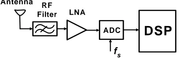
Low-cost and low-power receivers have gained importance due to increasing demands from wireless communication systems. In traditional digital communications, the RF signal is down converted to lower frequencies by means of analog mixers and filters. Current attempts in wireless communications are towards digitizing the received signal as close to the antenna as possible. Therefore, analog-to-digital converter (ADC) should be placed as near as possible to the antenna. After the ADC, with the use of robust digital signal processing (DSP) techniques, digital circuits will implement complicated filtering, down conversion and demodulation. In future receivers, antenna, LNA and ADC will be individual blocks only. All other functions will be processed in the DSP part. As a result a minimal set of RF and analog component will be required, as depicted in Figure 1.1. However, in such receivers, the ADC must achieve a high linearity in order to be able to digitize the input signal with minimal inter-modulation of interferers and exhibit a thermal and quantization noise floor well below the signal level at the output. The level of noise reduction varies different applications, which maybe in the range of 40-100 dB. For some applications a radio-frequency (RF) filter may be necessary to remove out-of-band noise so as to relax the dynamic range of the ADC.
DSP
ADC LNA
RF Filter Antenna
fs
Sampling receivers [1]-[3] are the primary attempts toward next generation receiver architecture. This dissertation focuses on designing a low power sampling PSK receiver for Mars orbiter-lander communication system in a deep-space environment. Deep space communication receivers must be robust to radiation hardness and Doppler effect as well. The receiver circuit is implemented in SOI CMOS technology to provide radiation hardening. SOI CMOS circuits exhibit performances superior to those of their bulk counterparts because of the following properties: the reduced parasitic capacitances, the absence of latch-up and its robustness against radiation hardness [4].
Sometimes the Doppler shift is several times wider in a space application for low data rates and often must be handled by circuit techniques. In an environment with a high Doppler shift, many modulation schemes require either pilot transmission technique or additional circuits [5][3] to handle the frequency shift. The proposed receiver uses a double differential technique with phase-shift keying (PSK) modulation to eliminate Doppler frequency offset. It requires no extra circuit such as pilot signal or PLL for carrier recovery [6][7], therefore resulting in high transmission efficiency and a simplified, low power circuit implementation.
The work presented in this dissertation is an effort towards a fully integrated PSK receiver for deep-space communication system in a deep space environment. And low power is one of the most critical priorities. All digital baseband circuit makes the design of low power receiver feasible. The power consumption in a digital CMOS circuit is P ∝ CVP
2
P
1.2. References
[1] C. Chien, R. Jain, E.G. Cohen, and H. Samueli, “ A single-chip 12.7 Mchips/s digitial IF BPSK direct sequence spread-spectrum transceiver in 1.2 µm CMOS,” IEEE J. of Solid–State Circuits, vol.29, pp.1614-1623, December 1994.
[2] F. J. Harris, C. Dick, M. Rice, “TDigital receivers and transmitters using polyphase filter
banks for wireless communications,”T IEEE Trans. Microwave Theory and Techniques,
vol. 51, pp. 1395-1412, April 2003.
[3] E. Gravyer and B. Daneshrad,“ A low-power all-digital FSK receiver for space applications,” IEEE Trans. Commun., vol. 49, no. 5, pp. 911-921, May 2000.
[4] J-P. Colinge, Silicon-on-Insulator Technology: Materials to VLSI. Kluwer Academic Publishers, 1997.
[5] W. Raffery and D. Divsalar, “Modulation and coding for land mobile channels,”
ICC’88, pp.1105-1110.
[6] M. K. Simon and D. Divsalar, “Doppler-corrected differential detection of MPSK,”
IEEE Trans. Commun., vol. 37, Feb. 1989.
[7] Y. Okunev, Phase and Phase-Difference Modulation in Digital communication. Norwood, MA: Artech House, 1997.
Chapter II
Low Power CMOS Wireless Communications: System
and Circuit Design Analysis
2.1. Introduction
In this section, we will explore many of the fundamental issues that arise in receiver designs. Early receiver circuits especially RF parts have been designed in GaAs, bipolar and BICMOS. Scaling down the dimension of CMOS technology has resulted in an increase in device bandwidth that has made possible the realization of RF circuitry. Due to its low cost advantage, designers have found it interesting to consider implementation of wireless receiver circuits in CMOS technology. Moreover CMOS technology resolves a number of issues such as substrate coupling, parameter variation with temperature and process [1].
2.2. Traditional Receiver Architectures
In traditional receivers, a front-end consists of single or multiple stages of down conversion, filtering and amplification of a RF transmission. The choice of a suitable wireless architecture should carefully be made because it can have a direct impact on the overall power consumption and performance. Besides low-power, the two most important specifications of a receiver to be considered are its selectivity and sensitivity. Selectivity of a receiver front-end is its ability to reject adjacent channels and image frequencies, while the sensitivity is its ability to detect weak signals at the receiver input such that a sufficient signal-to-noise ratio (SNR) will be obtain at the output of the receiver [4]. The most standard receivers are super heterodyne and homodyne receivers. They have been used for a long time, almost half a century. The homodyne receiver is also known as “zero-IF” or direct-conversion receiver [5] [6]. In the following sections, well-know conventional receiver architectures are discussed with advantages and disadvantages.
2.2.1
Heterodyne Receivers
LO1,
f
LO1LNA FilterIR
VGA
RF Filter
wc 0
DSP
ADC VGA
LPF
ADC
LO2,
f
LO2Q 90o Channel Select Filter Mixer LPF w wIF
-wIF 0
I
Figure 2.1. Heterodyne receiver architecture.
A frequency plan of the heterodyne receiver is illustrated in Figure 2.2. The undesired signal, called the image band, will be superimposed on the desired signal band after the two down conversion stages, as shown in Figure 2.2-(b). The role of the image-reject filter (IRF) together with the RF filter is to suppress the image band as much as possible [8]. There would be no need for a specific image-reject filter if the IF frequency is chosen sufficiently high so that the image band lies in the stop-band of the RF pre-selection filter. However, this is not the case for most heterodyne receivers. Amplification and filtering at high IF frequencies comes at the price of power dissipation.
fLO
- fLO
Im age D esired band f 2fIF P reselect “R F” filter
fIF -fIF Im age reject filter 0 f f a) b) c) C hannel select filter
Im age band interferer
Furthermore, it requires a large number of off-chip components that increase the receiver size. Almost all filters employed in heterodyne receivers are high-Q discrete filters-such as surface acoustic wave (SAW) or ceramic filters so as to obtain higher-quality channel-select filter [7].
From above discussion, heterodyne receivers depend on the trade-off between the image rejection and channel selection. The drawback of implementing off-chip components due to the required high Q image-reject filter is that it increases cost as well as power consumption. In addition, IR filter requires to be driven with 50Ω by the preceding stage-LNA. Driving a signal close to RF frequency for such impedance requires power hungry driver blocks [5]. Despite all above, heterodyne receivers have been most reliable receivers in wireless communications due to fact that they can sense the desired small signals even in the presence of large interferers. However, they have been limited to miniature, low-power and highly integrated transceivers.
2.2.2 Direct Conversion Receivers
The major driving force for direct conversion receivers is motivated by their cost, size and power reduction potentials. Direct-conversion receiver eliminates many off-chip components and offers significant power saving. The received signal is down converted to zero Hz or dc rather than a high intermediate frequency. The frequency of the LO signal is equal to the carrier frequency which means the desire signal and the image signal are the same. The advantage of this is that it relaxes or eliminates the need for the image rejection filters [5]. It has been used widely in digital cellular telephones, GSM receivers and miniature radio pagers [9][8].
DSP
ADC
LO, f
c
LNA LPF VGA
DSP
ADC LNA
VGA LPF
ADC
LO, f
c
VGA LPF
I
Q
90o
RF Filter
RF Filter wc
0 w
a)
b)
Figure 2.3. General schematic of direct conversion receiver, a) simple direct-conversion receiver, b) I/Q down
conversion direct conversion receiver.
The LPF can function as anti-aliasing filter and along with a variable-gain amplifier (VGA) they relax the dynamic range of the A/D converter. Despite its higher levels of integration, direct-conversion receivers may suffer from a number of issues that either don not exist or are not as serious in a heterodyne receiver.
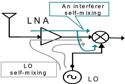
Direct–conversion receivers are very sensitive to LO feed-through that arises from capacitive and substrate coupling and bond wire coupling. Due to imperfect isolation between the LO and the inputs of the LNA and the mixer, a leakage signal, called “LO leakage,” appears at the inputs of LNA and the mixer which is mixed with the LO signal, as shown in Figure 2.4. This self-mixing (can be time-varying) produces a DC-component in-band and for some cases it may be stronger than the desired signal (i.e DC offset problem) [8]. This problem was the main reason why super heterodyne receivers have been more popular than direct-conversion receivers in many applications.
L N A
L O
L O s e lf - m ix in g
A n in t e r f e r e r s e lf - m ix in g
Aside from self-mixing problem, direct conversion receivers are exposed to flicker (1/f) noise since the desired signal is situated at low frequencies. Down conversion mixers and baseband circuits may introduce unexpected noise in narrow band that can impact the receiver performance. In addition to self-mixing and flicker (1/f) noise, second order distortion produces an unwanted tone that adds to the signal [7]. A power spectrum density, PSD of a down converted signal in a direct conversion receiver is shown in Figure 2.5.
P SD
f, frequency w hite noise, No
inform ation
1/f D C
Figure 2.5. A PSD of the down converted signal with impairment effects in down-conversion receivers.
Another serious problem associated with direct-conversion CMOS receivers is phase and gain imbalance of I/Q components for the receivers that use the scheme shown in Figure 2.3-(b). Most frequency and phase modulation architectures utilize a quadrature I/Q down conversion scheme because in general two-side bands of RF spectrum are different. The error in 90o shift and mismatch between I/Q components corrupts the detected signal, resulting in an increase in BER (Figure 2.6-(a))[11].
Figure 2.6. Impairment effects in 4-FSK down-conversion receiver, a) degradation due to I/Q phase mismatch
The DC offset degrades the receiver BER performance if it is not eliminated. Especially, for the modulation schemes which contain significant energy at and around DC. Figure 2.6-(b) shows the effect of DC offset on the BER of 4-FSK. As the offset level gets stronger, the BER becomes quite worse [12]. Several offset cancellation methods have been introduced to prevent all DC offsets [13][9]. Generally, the offset cancellation system has a very low bandwidth to eliminate the interference signals with the desired one. Direct-conversion receiver is the most preferable choice for the modulation that includes little energy around DC (e.g. 4-FSK or HQAM [14]). It can be suitable for wideband channels as well where a few kilohertz of the channel can be wasted which will not be that significant considering overall BER performance [7]. For narrowband applications, a suitable DC offset cancellation method must be used either in RF front-end with sort of ac coupling and filtering techniques or in the baseband with the DSP technique. Due to its excellent integration and low cost potential, direct-conversion receivers will continue to be used more often.
2.2.3.
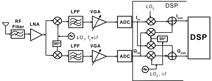
Low-IF Receivers
The goal behind low-IF is to combine the advantages of both heterodyne and homodyne receivers. It is well suited for full integration with high performance as well as reduced power consumption. It uses an IF frequency slightly higher than DC (e.g. a few hundred kHz) and is therefore not affected by DC offsets and 1/f noise. The IF frequency is chosen to be as low as possible so as to relax the requirements for the ADC. It is generally set to half the channel bandwidth so that the mirror signal is the adjacent channel. The image rejection is done on IF signal rather than RF, which exhibits excellent integration, because the image rejection and the channel selection no longer require high-Q filtering [15].
DSP
ADC LNA
VGA LPF
ADC
LO1, fc+ f
VGA LPF
Iin
Qin
90o
RF Filter
LO2 , f
∆
∆
LO2
90o
DSP
Iout
Qout
Figure. 2.7. A low-IF receiver.
Wide-band IF or Low-IF Receiver with Double Conversion Receiver
There exists another architecture which is well suited building for highly integrated receiver known as wide-band IF architecture [3]. A wide-band double-conversion IF receiver is shown in Figure 2.8. This architecture is similar to that of given in Figure 2.7 except that here the IF frequency can typically be high. Also, it does not require a higher resolution ADC as in that of low-IF because the ADC comes after when image band is eliminating. After the prefilter and LNA, the RF signal is down converted to IF via first quadrature down conversion. A wide-band filter is used at IF to translate all of the received channels to the second stage of mixers. All of the channels are then transferred to baseband using channel select filters. Finally, the selection of the desired signal is performed at baseband with digitally programmable filtering. In the second complex mixing, by adding the outputs of the real multiplier in pairs, the image band is cancelled [3].
DSP
ADC LNA
VGA ADC
LO1,
fc+ fIF
VGA
Wide-band LPF or BPF
I
Q
90o
RF Filter
LO2 , fIF
Channel select
filter
cos(wLO2t)
cos(wLO2t)
sin(wLO1t)
Figure 2.8. A wideband double-conversion IF receiver.
2.2.3 a) Image Rejection in Low-IF and Wide Band IF
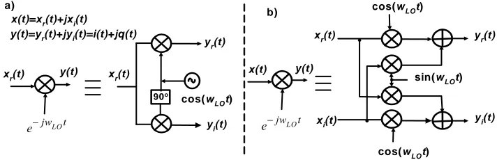
In low-IF and wide band IF receiver, the image rejection is achieved at IF level with the solution of integrated on-chip. The IR filter used in these architectures is similar to Weaver technique [18][7]. Avoiding the image band is based on the theory of mixing with a complex exponential rather than mixing with a real signal. As an example, down conversions illustrated in Figure 2.9 are accomplished by using a complex exponential signal. The input signal in Figure 2.9-(a) is a real signal while the input signal in Figure 2.9-(b) is a complex signal. The resulted spectrums of mixing for both cases are shown in Figure 2.10. As can be seen, there is no image problem for such down conversions [16][14]. On the other hand, the suppression of the image in this image rejection technique is limited by the quadrature accuracy of mixer input phases and gain matching of the mixers.
cos(wLOt)
cos(wLOt)
sin(wLOt)
t jwLO
e−
cos(wLOt)
90o
t jwLO e−
x(t)=xr(t)+jxi(t)
y(t)=yr(t)+jyi(t)=i(t)+jq(t)
xr(t)
yi(t)
yr(t)
xr(t)
y(t)
xr(t)
xi(t)
x(t) y(t)
yr(t)
yi(t) b)
a)
0
w
w
- w LO
0
w
w X r ( w )
Y ( w )
X ( w )
Y ( w )
-wLO wLO
a ) b )
Figure 2.10. The spectrums of the inputs and outputs of down conversion mixers, a) the mixing of a real signal
with an exponential signal, b) the mixing of a complex signal with an exponential signal.
The realization of I/Q down conversion mixers used for the IR filter is done with polyphase filters. Those filters are usually band-pass filters that have a pass-band at either positive or negative frequencies. A circuit implementation of this filter with the active-RC filter can be found in [16]. Quite interesting and digital implementations of such image-rejection filters or aliasing filtering have also been introduced in [19][20].
2.2.4.
Digital-IF Receivers
Current goal for receiver designers is to eliminate the analog signal processing or to replace them with digital counterparts. This would only be achieved by directly digitalizing the signal right after antenna, and performing all the operation in the digital domain. With the use of robust digital signal processing (DSP) techniques, digital circuits will implement the complicated filtering, down conversion and demodulation. For such application, the ADC would require at least 16-bit resolution and would need a dynamic range of more than 100 dB at 0.8-2 GHz frequencies [24][25]. Such an ADC is not practical in current technology. Even if they can be designed, the power consumption will be the fundamental limitation. As an example, a 7-bit ADC with the speed of 1 Gs/s consumes a power of 1.75 W [24], which is not acceptable for a low power application. The digital–IF architecture was a step toward SDR idea wherein the last down conversion stage in heterodyne receivers is replaced by an ADC. This idea is sometimes called IF-sampling [23]. If the sampling frequency is chosen very less than the IF frequency, it is then called subsampling [26]. This approach will be discussed more in detail as both architecture and system level later in the next section. We will also introduce some of our studies on this subject through this dissertation.
2.3. Next-Generation Receiver Architectures
In previous section, we have discussed some traditional receivers that are currently employed in many radio applications. In this section, we will introduce some of new architectures that have been targets of receiver designers for last two years. And many attempts are towards these architectures due to their excellent properties and answer the demands from industry. The recent increasing demand from wireless communications to IC designers is to design extremely flexible receivers that can support multiple standards.
wide range of frequency bands and channel bandwidths [27][28]. This is a unique problem and critical feature of next generation wireless receivers. Unlike traditional narrow band receiver architectures, here the LNA and the ADC will be exposed to a large number of carriers and channel bandwidths. Wide band LNA’s have already been active research subject [29][30] and more such LNA designs will be seen in near future in the publications of the IEEE Solid-State Circuit Society. The signal dynamic range as well as the number and power of the interferers determine the performance of an ADC. In future wireless communications, all of filtering will be done in digital domain on-chip and perhaps only the RF passive filter will be the necessary off-chip component. Digitizing the received signal will be achieved with a high performance and wide band ADC.
U
Advance in ADC
The most important key of the success in next generation receiver is definitely the advance in the ADC. The rapid evolution of integrated circuit processing enables the scaling of technology feature sizes to smaller dimensions. A fundamental figure of metric to evaluate the impact of the technology scaling on analog circuits is [31][24]
pation PowerDissi
Bandwidth x
ge DynamicRan
FoM = (2.1)
Applying this to an ADC will result in the following:
diss s N
P f
FoM = 2 (2.2)
where N is the quantization bits, fBsB is the sampling rate and PBdissB is power dissipation. The
measure of the ADC performance is PBerfB= 2P N
P
fBs. B The figure of merit for the ADC emphasizes
Figure 2.11. Power efficiency of ADC’s [31].
Although progress has been made in terms of power efficiency in ADC’s, the same is not true for the resolution and power dissipation. High performance ADCs dissipate more power. Another survey shows that an average improvement is only ~1.5 bits in the resolution for six to eight years [24]. Figure 2.12 shows log-log relationship between the increased resolution and dissipated power in ADC’s [32]. The results have indicated that little improvement has been made over a period of 8 years. ADC’s with wide bandwidth and high resolution required for next generation receiver architectures are at present unfeasible and consume too much power [25]. As an example, two examples that would represent Today’s state_of_art are 13-bits, 10Ms/s, 1.1W and 7-bits, 1Gs/s, 1.75W [24].
2.3.1. Software-Defined Radio (SDR) Receivers
A multi standard receiver should have enough flexibility and programmability to be applied to different standards. The concept of software-defined radio (SDR) is an emerging technology enabling the development of flexible multistandart/multiuser systems, reconfigurable and adaptable by software. This flexibility is achieved by performing all of signal processing in software [33]. The front-ends suitable for software radios must have wide bandwidths to accommodate a large range of frequencies.
The original idea in SDR is to place the ADC right after the antenna, as depicted in Figure 2.13. This ideal front-end is limited by the Today’s technology due to difficulties in designing high dynamic range ADC structures, as discussed above. Instead, current designs are mainly focused on digital-IF architectures [32][34].
Software controlled
DSP (FPGA’s, ASIC, etc.)
ADC LNA
RF Filter Antenna
fs
Figure 2.13. An ideal SDR configuration.
2.3. 2. Ultra-Wide Band (UWB) Receivers
A general UWM transceiver is shown in Figure 2.15 [38]. The choice of a modulation scheme will affect the architecture of UWB receivers. There are different modulation schemes proposed for UWB systems - pulse position modulation (PPM), pulse amplitude modulation (PAM), binary shift keying (BPSK) on-off keying (OOK), as shown in Figure 2.16 [39]. The main concern regarding UWB waveforms is the potential interference that they can cause to specific critical wireless systems.
Sinusoidal, narrowband
Pulse, ultra-wideband
Time Frequency
Time
Figure 2.14. Waveforms and spectrums of conventional communication systems and UWB systems [38][36].
1 0 1 0
Figure 2.16. Different modulation techniques for UWB pulses, a) OOK, b) PAM, c) BPSK, and c) PPM.
The motivation for UWB can be understood by looking at Shannon’s well-known channel capacity equation [40]
) 1 ( log2
N S W
C = + (2.3)
where C is the maximum channel capacity (bits/sec) of an additive white Gaussian noise (AWGN) channel, W is the channel bandwidth (Hz), N is the noise power, and S is the signal power. As can been seen from (2.3), the channel capacity C is linearly dependent on the bandwidth W, whereas it increases only with the logarithm of the signal-to-noise ratio (SNR)
S/N. In UWB systems the available bandwidth W is quite high (W≥1GHz), and therefore low transmitted power or low SNR is required. UWB technology seems to have great potential for future high-capacity wireless systems [37].
2.3. 3. MIMO Receiver Architectures
M ultipath fading :
intersym bol interference co-channel interference
Figure 2.17. MIMO communication architecture.
) / / )( 1
(
log2 SNR b s Hz W
C = +
(2.4)
A spectral efficiency of a MIMO, N Tx and M Rx antennas for an unknown channel is
) 1
( log2
N M SNR N
W C
+
= And if N = M Nlog2(1 SNR)
W C
+
= (2.5)
As can been seen, the spectral efficiency of a MIMO channel grows approximately linearly with the number of antennas. Figure 2.18 shows some examples for antenna diversity. MIMO systems have a better capacity at high SNR while conventional RX schemes are more attractive at low SNR values [42]. Due to its complex structure, a receiver circuit for MIMO system will be cost and power inefficient. For example, 4-channel diversity for quadrature-amplitude modulation (QAM) receiver [43] consumes 1.1 W at 3.3 v where most of front-end, RF and IF sections were not included in the chip.
2.4. Alternative Front-end Architectures for
Wideband Receivers
New wide-band receiver technologies such as ultra-wide band (UWB) and SDR have made it necessary to sample at much higher rates than the current ADCs allow. As we discussed earlier, the wide dynamic range requirement and high power consumption make it difficult and unfeasible at present to employ a Nyquist-rate ADC in wideband front-ends. Nevertheless, the performance limitation of ADC’s can be alleviated by incorporating subsampling technique [23][44]. This approach does not only relax the ADC requirement but also eliminates some of analog down conversion stages.
2.4.1. Subsampling Front-end via ADC’s
The subsampling process is often called bandpass sampling due to applying the Nyquist Criterion to bandpass signals. It samples the bandpass signal dependent upon the signal’s bandwidth rather than its position [44]. In particular, it behaves like a mixer by sampling the input RF signal at a frequency that is lower than the carrier but at least twice of data rate. Therefore, traditional analog down conversion components can be eliminated by the sampling process. The effect of Nyquist sampling on a lowpass bandlimited signal and bandpass signal in the frequency domain is shown in Figure 2.19. According to the sampling theorem, the spectrum of the original signal is repeated at integer multiplies of the sampling frequency after sampling a lowpass signal, as illustrated in Figure 2.19-(a).
fs > 2fbmax fs > 2B and fs = fc / M
+ fbmax
- fbmax
+ fbmax
- fbmax +f
s -fs
….. …..
0 fim= +fs/2
+fs/4
+3fs/4
-fs/2 -fs/4 +fs
+fc
-fc
….. ...
B
a) b)
Sampled signals
0 Desired signal Interference
“undesired” signal
R (f )
Rs (f )
R(f)
Rs ( f )
RF filter
The sampling rate must be at least two times the highest frequency component of the analog signal (i.e. fBs B≥ 2fBmaxB) to avoid the loss of information [45]. However, for the bandpass
sampling, the sampling frequency has to be at least two times the bandwidth of the information to prevent aliasing (i.e. fBs B≥2B). To sample a bandpass signal without a spectrum
overlap, the relation between the sampling frequency fBsB and the carrier, fBcB is given by 1 , 2 and 1 2
4 = >>
+
= n f fs B n
fs c (2.6)
The images resulted from subsampling are located at the frequencies fBim B= (kfs B B± fBcB), where k
is an integer number [44]. Using (2.6), the spectral images (Figure 2.19-b) will be located at
fBim B= (k ± 1/4)fBsB.B B(2.7)
A problem arises in practice at the front-end of a receiver due to the fact that the front-end RF filter (that is usually a bandpass filter (BPF)) cannot remove all of the out-of-band interference completely. Therefore, during transferring the replicas of the signals, the undesired interference signal may overlap with the desired signal (Figure 2.19-b.). The relative power of the desired signal to the interference (signal-to-interference ratio) is important for the system performance. If fBs B= KBbfBBbB, where fBb Bis the information rate or “bit”
frequency, and then the number of samples taken by the ADC is
b in b
s b
s f T
n T f f f K 1 2 4 + = =
= (2.8)
where TBbB is the duration of symbol.
A practical issue associated with sampling front-end is its sensitivity to the jitter due to the sampling clock that can cause degradation on the system performance. The aperture jitter on the sampling clock results in phase noise and its spectral density is amplified by MP
2
P
[26]. A jittered clock can create interference in the desired band caused by the adjacent channel. The power density of the interference signal will be greater with a higher phase noise clock. So a lower phase-noise oscillator is required in a subsampling system for the sampling clock generation. The maximum allowed input frequency of the ADC will also be limited by aperture jitter. The ADC’s SNR imposed by sampling jitter can be specified by [46]
where ta is the aperture jitter for the sampling clock. As can be seen, even the system is operating at a frequency lower than the input frequency fin in subsampling front-end, the jitter is still a function of fin. The theoretical SNR degrades as the input frequency increases. Typical range of the jitter in practical ADC’s has been 1-2 ps [24]. As an example for a 500 MHz input signal (fsample/2=500MHz), the SNR due to the clock jitter will be 44 dB. The
defined two problems (the overlapped noise and clock jitter) associated with subsampling systems are only significant when the subsampling coefficient M is very large. However, if the input signal frequency to the ADC, fin, is low enough (by using one down conversion stage to decrease the carrier frequency), then those two effects can be ignored.
Another non-ideality that affects the ADC’s SNR is the quantization noise. The dynamic range due to the quantization noise is given by [24][45]
SNRq = 6.02N+1.76+10log(fs /2fbmax) (2.10) where N is the resolution bits and fbmax is the maximum frequency of the input signal. Usually
fs = 2fbmax and then the SNR=6.02N+1.76. Notice that, the dynamic range of the ADC can be increased by increasing the number of bits. With respect to the type of the modulation scheme is used, in order to obtain a reasonable system bit-error rate (BER) performance, the non-idealities (2.9) and (2.10) have to be taken in consideration for the design of the receiver’s ADC.
2.4.2. (Sub)-Sampling Receiver Architectures
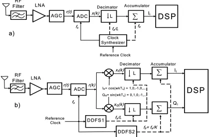
ADC LNA
DSP
LNA ADC Accumulator Ii Qi RF Filter RF Filter a) b)IR= cos(wkTs) = 1,0,-1,0,….
QR= sin(wkTs) = 0,1,0,-1,….
Decimator L L r(t) r(k) L Decimator Accumulator
∑
DSP
∑
Ii∑
fs fs x(k)xI(k)
xQ(k)
r(t)
fb
fs/L
Clock Synthesizer
Reference Clock
DDFS1 fs/L
DDFS2 fb= fs/K
Reference Clock
AGC
AGC
Figure 2.20. General schematic of subsampling receivers, a) simple direct-subsampling receiver, b) I/Q down
conversion direct-subsampling receiver.
If the sampling frequency for this receiver is chosen as given in (2.6), then the subsampling ratio M = fBcB/fBs B= (2n+1)/4. Choosing the sampling ratio as (2n+1)/4 provides the signal to be
sampled at the values of 1,0 and -1, resulting in significant reduction in hardware complexity in a receiver front-end. The reference signals in Figure 2.20-(b) are given as the followings:
,... 0 , 1 , 0 , 1 , 0 , 1 , 0 , 1 ) 2 cos( ) 2 cos( )
(k = f kT = kM = − −
IR π in s π k=0,1,2,3,… (2.11-a)
⎟⎟ ⎠ ⎞ ⎜⎜ ⎝ ⎛ = − = − = = = odd n even n kM kT f k
QR in s
,.. 1 , 0 , 1 , 0 ,.. 1 , 0 , 1 , 0 ) 2 sin( ) 2 sin( )
( π π k=0,1,2,… (2.11-b)
The IBRB and QBRB components are generated by a numerical control oscillator (NCO) digitally
and consist of the values of 1,-1, and 0. This dramatically simplifies the design of the digital mixer. At the outputs of the digital mixers, signals are
,.. 2 , 1 , 0 ,... 0 ), 2 ( , 0 ), 0 ( ) ( ) ( )
(k =r k I k =r −r k =
xI R (2.12-a)
,..0,1,2
),... 3 ( , 0 ), 1 ( , 0 ),... 3 ( , 0 ), 1 ( , 0 ) ( ) ( ) ( ⎟⎟ = ⎠ ⎞ ⎜⎜ ⎝ ⎛ − − = = k r r r r k Q k r k
At the outputs of the accumulators: ) ( / k x I L b K I i k
∑
= and .
/ ) (
∑
= L b K Q i k k xQ (2.13)
where K=fBsBT/L, the number of samples at the accumulators in a symbol duration TBbB, and L is
the decimator rate. Note that each accumulator has to be reset periodically (every TBbB =1/fBbB
period) in order to realize uncorrelated samples Sincethe signal is not downconverted to zero frequency (fBimB≠ 0) in direct conversion receivers, the problems associated with the traditional
analog architectures such as DC offset problem, flicker noise (1/f ), and I-Q mismatches are negligible.
2.4.3. IF (Sub-) Sampling Receiver Architectures
Although with increase advance in VLSI technology, the idea of direct subsampling is very attractive for some practical applications (e.g. short distance and low-speed communications). In high-speed applications (fBcB>1GHz), however, it is not practical due to
limited dynamic range of the ADC in Today’s technology. For such applications we suggest using one down conversion stage before the sampling to relax the Q of the IF BPF filter (i.e. IF subsampling), as indicated in Figure 2.21. The IF amplifier provides adequate gain to the input signal to ease the ADC requirement. The ADC dynamic range is arranged by the gains of LNA and IF amplifier. Notice that the signal is amplified by a LNA and an IF amplifier with only the LNA is working at carrier frequency. However, for direct-subsampling approach, the high gain required at the RF stage is provided by a high gain LNA.
DSP
LNA ADC Accumulator I Q RF FilterIk= cos(wkTs) = 1,0,-1,0,… .
Qk= sin(wkTs) = 0,1,0,-1,… .
Decimator L L r(t) r(k) ∑ ∑ fs
xI(k)
xQ(k)
DDFS1 fs/L
DDFS2
fb= fs/K
Reference Clock Image Reject or IF Filter RF Frontend IF Amplifier IF Digital Processing IF BPF VCO
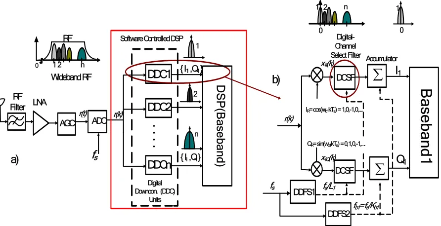
In wide-band receivers, the receiver circuit must have the ability to detect different data rates. In Figure 2.22, the subsampling receiver architecture for wide-band multi-standard receivers is shown. It is capable of detecting the signals with variable data-rate. The channel selection is done in the digital domain by means of a programmable digital channel select filter (DCSF) unit. In order to support a wide range of data rates, one or more decimation stages are used to select each channel, as shown in Figure 2.23. The appropriate parallel decimation stage is selected by a control signal from symbol timing circuit according to the desired data. LNA ADC RF Filter a) r(t) fs DDC1 DDC2 DDCn
Software Controlled DSP
Baseband1
Accumulator
I1
Q1
IR= cos(wc1kTs) = 1,0,-1,0,….
QR= sin(wc1kTs) = 0,1,0,-1,…. Digital-Channel Select Filter
∑
∑
DDFS1 fs/L1DDFS2fb1= fs/Kb1 DCSF
DCSF x1I(k)
x1Q(k)
DS P(Ba se ba nd ) fs Digital Downcon. (DDC)
Units
b)
r(k) r(k)
{ I1 ,Q1 }
{ Ii ,Qi }
Wideband RF
1 2 n
RF 0 2 1 n 1 0 2 0 1 n AGC
Figure 2.22. A subsampling architecture for wide-band digital receivers, a) a multi-standard radio architecture,
b) digital down conversion (DDC) at each stage.
D C S F f
b1
=
C on tro l sign a l L1
L 2
L3
fb 2
fb3
. . fb i L
D ecim ation F ilte r
=
T o a ccu m ulato r
Figure 2.23. Cascaded decimation filter structure for multirate in wideband digital radio. The channel-select
Due to limited dynamic range of the ADC in Today’s technology, one down conversion stage might be needed before the sampling to relax front-end dynamic range (i.e. IF subsampling), as indicated in Figure 2.24. The wideband RF signal is amplified and down converted to a sufficiently high IF frequency that cover all necessary multi-bands (i.e. wideband-IF). The role of the image-reject filter (IRF) together with the RF filter is to suppress the undesired image band as much as possible. Due to their high level integration, IR filter can be realized by using the quadrature complex filter or polyphase filters [3][16].
LNA ADC RF Filter r(t) fs Reference Clock Image Reject or IF Filter Wideband RF Frontend (0.8-2 GHz) IF Amplifier Wideband-IF Digital Processing IF BPF VCO DDC1 DDC2 DDCn DSP (Ba se ba nd) Digital Downconversion (DDC) Units r(k)
{ I1 ,Q1 }
{ Ii ,Qi }
DDFS
1 2 n
RF
0 1 2 n
IF
0 fIF 1
(100-200 MHz)
Figure 2.24. An IF (sub)sampling multi-standard receiver architecture.
The DCFS unit not only selects the channel but it also decreases the number of samples in a manner that a constant-sized accumulator can be used for each data rate, resulting in significant reduction of the complexity. At the input of DCFS the data are fb1, fb2…, fbi , where
fb1> fb2...> fbi.The numbers of samples at the output of the DCFS for each channel are then
K = Kb1 = [fsTb1/L1] = Kb2 = [fsTb2/(L1.L2] =
L = H(z)
fs/L
F L Z Z L z H ⎥ ⎥ ⎦ ⎤ ⎢ ⎢ ⎣ ⎡ − − − − = 1 1 1 1 ) ( order Decimation ratio Z-1
If
Z
=
e
jw j F L Fw L wL e w H ⎥ ⎥ ⎦ ⎤ ⎢ ⎢ ⎣ ⎡ − − = ) 2 / sin( ) 2 / sin( )
( ( ( 1)/2)
,
Z-1
fs/L
Z-1 Z-1
Decimation Filter
F
Figure 2.25. A Comb filter implementation as a decimation filter.
Shown in Figure 2.26-(a) is the typical frequency response of a Comb filter employed as a decimation filter. A cascade of F = 6 (sixth-order) comb filters with decimation ratio of LB1 B=
8 and LB2 B= 32 are considered. The sampling frequency is chosen as 128 MHz. As clearly
seen, the cascaded structure in Figure 2.23 will exhibit a filter with variable passband. This cascaded structure can be designed to meet different standards with multiple data rates. If the passband defines the channel bandwidth (fBbiB), then it becomes smaller when higher
decimation stages (or more cascaded structure) are used, which corresponds to lower data rates. Thus the length L defines the bandwidth of the filter. For example, fBb1B (LB2 B=32) <fBb2B (LB1
B
=8), as depicted in Figure 2.26(a). B
The filter order F provides aliasing attenuation. Figure 2.26-(b) shows frequency responses of comb filter with different orders (F=4, 6, and 8). As can be seen, increasing the number of stages in the Comb filter improves the alias rejection. As a part of filter design, L and F can be arranged such that an acceptable pasband characteristic with adequate aliasing attenuation can be provided.
fs/2=
64 MHz
F=4, L=8 F=6, L=8 F=8, L=8
dB
fs/2
16 32 48
f (MHz)
- 51 dB
- 77 dB
- 128 dB
fbi
Magn
itude
,
dB
f (MHz)
L1=8, F=6
L2=32, F=6
16 32 48
4 f
s/2
b) a)
Figure 2.26. Frequency response of Comb filters, a) cascaded Comb filter for different decimation rates, b)
frequency responses of 4, 6 and 8-order Comb filters (fs =128 MHz).
2.5. Key Parameters in Designing Low-power and
High Performance Transceivers
In this section we will describe steps that will be help full to design a receiver for specific applications. To find an optimum design solution, it is necessary to consider the entire communication system with both theoretical and practical point of view. This requires the involvement and understanding of communication theory (e.g. modulation techniques, baseband, signal processing, coding, etc.), integrated circuit (IC) technology, analog, RF and digital circuit design, mixed-signal design issues, and layout issues. Therefore receiver design requires a highly multidisciplinary task. Two most important parameters that a receiver is designed for are the bit-error rate (BER) performance and power consumption. The followings are major parameters that need to be defined in order to start the design of a receiver.
1-Transmit and receive power 2-Channel effect and channel loss
3-Receiver sensitivity and dynamic range 4-Modulation type
5-Bit rates
1-Transmit and receive power
The basic expression for the relationship between the received power and the transmitted power for a radio communication system is expressed as [10]
2
) / 4
( πd λ
G G P
P T T R
R = (2.15)
where PBRBis the received power level,BBPBTB is the ransmitter power, GBTB is the tranmitter antenna
gain, GBRB is the teceiver antenna gain, d is the distance between the receiver and transmitter
and γ = c/fBcBis the wavelength of the transmitted signalB, Bc is the speed of the light and fBcB is the
frequency of the transmitted signal. The factor LBsB=(λ/4πd)P
2
P
is called the free-space path loss. The received power can be written in dB as
(PBRB)dB=(PBTB)dB + (GBTB)dB +(GBRB)dB+(Ls)dB (2.16)
From the above equation it is clear that the most crucial parameters that define the power level of the received signal is the tranmitter power and the path loss. Designing a low power receiver circuit is directly related to the power level of the received signal. Especially, for short distance communication links, the tight requirements of a receiver circuit are relaxed because of the possibility of obtaining high signal level.
2-Channel effect and channel loss
Transmission of digital information is usually considered through an additive Gaussian noise channel (AWGN) and so is the communication system design. The maximum capacity of an AWGN channel can be defined with Shannon’s well-known channel capacity formula [40]:
) 1
(
log2 SNR
W
C = + (2.17)
As can been seen from the above equation, in order to obtain the maximum spectral efficiency of the channel, the transmitted bandwidth (i.e. transmitted data rates) has to be compensated with SNR.
The thermal noise that observed at the receiver front-end causes an additive Gaussian noise which has a flat power density spectrum:
0
0 K T
N = B W/Hz (2.18)
where KBB B= 1.38 X 10P
-23
P
is the Boltztman’s constant and TB0B is the noise temperature in
Kelvin. The total noise power in the signal bandwidth is NB0BB, where B is the bandwidth of
3-Receiver sensitivity and dynamic range
Two of the most common measures of a receiver performance are sensitivity and dynamic range. The receiver sensitivity can be found by using the equation [1],
S= N0(B)SNRReqNFT. = -174 dBm/Hz+ (B)dB+ (SNRReq) dB+ NFT (2.19) Here, N0 is the thermal noise, NFT = SNRin/SNRout is the total noise figure , SNRReq is the
required SNR to get a good performance of BER, and B is the channel bandwidth. Most published receivers have an total noise figure from 3 dB to 6 dB. The sensitivity of a receiver is defined as the minimum signal level that the system detect with the required SNR. If the signal detected at the front-end is well above the sensitivity level for the worst cases, then a recever design with high noise figure can be tolerated. Bluetooth receivers are such applications where the minumum signal at the receiver is supposed to be high and so is the noise figure [48]. Such a sytem is easy to design and will consume lower power. If R is data rate (R=1/T), the receiver dynamic range is calculated as follow.
PR = (R)dB + (SNRreq)dB + (N0) dBm (2.20) As can be understood from the above equation, for higher data rates, higher dynamic range is required. The sensitivity and dynamic range depend on the modulation scheme because the required SNR, SNRReqwill be defined differently for a threshold value of BER in different modulation schemes.
4-Modulation type
![Figure 2.12. ADC power dissipation versus resolution [32].](https://thumb-us.123doks.com/thumbv2/123dok_us/1354199.1168268/32.612.135.499.71.295/figure-adc-power-dissipation-versus-resolution.webp)
![Figure 2.15. UWB transceiver architecture [38].](https://thumb-us.123doks.com/thumbv2/123dok_us/1354199.1168268/34.612.120.497.213.472/figure-uwb-transceiver-architecture.webp)
![Figure 2.18. Channel capacity of MIMO vs single conventional receiver [42].](https://thumb-us.123doks.com/thumbv2/123dok_us/1354199.1168268/36.612.143.488.494.700/figure-channel-capacity-mimo-vs-single-conventional-receiver.webp)