Available online: https://edupediapublications.org/journals/index.php/IJR/
Page 4059
A New Approach for Design of 10T SRAM Using Half-V
DDPrecharge and Row-Wise Dynamically Powered Read Port
Farheen Maryam 1, Naela Husna 2
1,2Assistant professor, Dept. of ECE, RamanandaTirtha Engineering College, Nalgonda,Andhra Pradesh, India
Abstract:We aim, in this paper, a brand new 10T static random access reminiscence cellular having single-ended decoupled read-bit line (RBL) with a 4T examine port for low power operation and leakage reduction. The RBL is precharged at half of the cell’s supply voltage and is authorized to cost and discharge in accordance with the saved data bit. An inverter, pushed by the complementary statistics node (QB), connects the RBL to the virtual energy rails through a transmission gate in the course of the read operation. RBL will increase closer to the VDD stage for an examine-1 and discharges toward the ground level for a read-zero. Virtual strength rails have the same cost of the RBL precharging level during the write and the maintenance mode and are linked to true deliver levels most effective at some stage in the study operation. Dynamic manipulate of digital rails drastically reduces the RBL leakage. The proposed 10T cell in an industrial sixty-five nm generation is 2.47× the scale of 6T with β=2, presents 2.3× examine static noise margin, and decreases the examine strength dissipation with the aid of 50% than that of 6T.
Keywords-10T, charge recycling, leakage reduction, low power, precharging, single ended (SE) read bitline (RBL), static random access memory (SRAM), virtual rails.
I. INTRODUCTION
The principles of operation of SRAM, their design considerations, and the techniques that are used to reduce power dissipation in SRAM are discussed here. Static memory cells basically consist of two back to back connected inverters as seen in Fig.1. The output of the second inverter (Vo2) is connected to the input of the first inverter (Vi1).If we consider the voltage transfer characteristics of the first inverter
(Vo1 verses Vi1) and that of the second considering Vi2=Vo1 as shown in Fig. 2a and Fig.2b respectively, there are three possible operating points (A, B and C) obtained by intersection as shown in Fig. 2c. It may be seen that operation points A, B are stable as loop gain is less than 1. Point A shows that the output of inverter1 is high and the output of the inverter2 is low. Point B shows that the output of inverter1 is low and the output of inverter 2 is high. This shows that the outputs of two inverters are complementary in any stable condition. This property is made use of to realize static random access memory SRAM.
Point C is a meta stable operating point as the loop gain at point C is much larger than 1. When a small deviation is applied to the input of the first inverter when the operating point is C, it gets amplified by the gain of the first inverter and is applied to the input of the second inverter and again amplified by the gain of the second inverter. The values of Vo1 and Vo2 (Vi2) increases and the bias point moves away from C until it reaches either A or B..The curve in Fig.2c is also known as Butter fly curve.
Available online: https://edupediapublications.org/journals/index.php/IJR/
Page 4060
Many investigations have been completed to lessen the power dissipation in SRAM, to broaden low electricity and strength green SRAM. Many of those cowl SRAMs operated at low voltages decreasing electricity dissipation, SRAMs using strategies like power gating wherein the circuits are switched off when they're no longer needed, SRAMs (drowsy) where the electricity supply voltage is decreased to a lower fee throughout standby mode and SRAMs based on adiabatic techniques. Lowering the energy supply voltage reduces the dynamic energy quadratically and leakage electricity exponentially. But strength deliver voltage scaling additionally limits sign swing and hence reduces noise margin. Further, competitive technology scaling in the sub-100nm region increases the sensitivity of the circuit parameters to technique variation (PV). Leakage currents are in particular because of gate leakage cutting-edge and subthreshold leakage current.
High K gate era decreases the gate leakage present day. Forward frame biasing methods and twin Vt
strategies are used to reduce subthreshold leakage modern. In sub-threshold SRAMs, electricity deliver voltage (VDD) is lower than the transistor threshold voltage (Vt) and the subthreshold leakage current is the operating modern. Jaydeep P. Kulkarni et.Al proposed Schmitt Trigger SRAM cellular that contains a built-in the feedback mechanism, achieving 5-6 % improvement in SNM, improvement in manner version tolerance lower read failure possibility, low-voltage/low electricity operation, and stepped forward statistics retention capability at the extremely low voltage in comparison to traditional 6T SRAM cellular. They file that at iso-region and
iso-study-failure probability the proposed
reminiscence bit mobile operates at more alow (one hundred seventy-five mV) VDD with 18% discount in leakage and 50% discount in examine/write power as compared to the traditional 6T cellular. As in step with their simulation outcomes, the proposed reminiscence bit cell keeps records at a supply voltage of one hundred 50mV. Naveen Verma et.Al delivered 8T bit-cell with the buffered study which removes the read SNM limitation. Added to it the peripheral footer circuitry removes bit line leakage. The peripheral write drivers and garage-mobile
deliver drivers designed by way of the authors have interaction to lessen the cellular deliver voltage in the course of write operations. Sense-amp redundancy provided produces a favorable exchange-off between offset and location. The SRAM array constructed with 65nm technology became discovered to be useful at 350mV and data correctly retained at 300mV. Fatih Hamzaoglul et.Al presented a 153Mb SRAM design optimized for 45nm high –K steel-gate era. The layout as put forward with the aid of the authors carries fully integrated dynamic forward-frame -bias to achieve decrease voltage operation even as preserving low the vicinity and energy overhead. The dynamic sleep design used with op-amp -based feed-returned control and on-die programmable reference voltage generator reduces the effect of procedure versions and decreases the strength. They claim that the layout operates over 4.5GHZ at 1.1V and the more potent PMOS under the forward body bias improves the operating voltage as much as 75mV, without increasing the leakage energy. The excessive K cloth almost gets rid of gate leakage within the cell and makes this design appealing for low strength programs. Y. Wang et.Al proposed a 1.1 GHz 12μA/Mb SRAM layout in 65nm ultra–low electricity CMOS generation with included leakage reduction technique for cellular applications. They rent gate oxide thickness optimization and gate nitridation to reduce gate leakage. Well, and pocket implants and source-drain spacers are optimized
concurrently to reduce subthreshold leakage.
Separate Vt threshold voltage manipulates for N and
P transistors in SRAM cells and the peripheral circuit is employed to get minimum Vmin. The mobile size is optimized to get excessive array efficiency of 7-8% and bit performance of 115Mb/cm2 for 128kb sub
array with improved static noise margin, write margin and read current at low-voltage design factor. Transistor stacking and lengthy channel transistors are used to keep standby leakage in peripheral circuits.
II. SUGGESTED SCHEME
A. 10T Cell:
Available online: https://edupediapublications.org/journals/index.php/IJR/
Page 4061
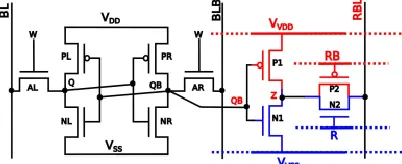
in Fig. 3. We have added a 4T read port to the 6T cell to decouple the internal nodes during the read operation. Read port consists of an INV P1-N1 driven by node QB, and a transmission gate (TG) P2-N2. The output (Z) of the INV is connected to RBL during the read operation through TG, which is controlled by (read) control signals. Furthermore, read port is powered by virtual power rails, VVDD and VVSS, which are dynamically controlled. These virtual power rails (control signals) run horizontally, and have the true rail values only during the read operation. For the RBL leakage reduction, both the virtual rails have the same level as the precharge level of RBL.
The 10T SRAM cell using an INV and a TG has been proposed earlier [33]. However, our proposed 10T scheme is different from the previous design in the following aspects.
1) The previous INV+TG-based 10T cell was application specific, while our proposed design is generic.
2) We have used the dynamically controlled power rails for the read port.
3) We precharge RBL at VDD/2, while the previous 10T design eliminated the precharge phase, and used INV to fully charge or discharge the RBL.
4) The basic read technique of both the designs is completely different. The main idea of the proposed design is “the charging or the discharging of the read BL from VDD/2 for every read operation.” The previous design either discharges from VDD to VSS, or charges from VSS to VDD.
5) A powerful INV was used previously to produce full VDD swing on the RBL. In the proposed design, RBL is precharged at VDD/2, and only a small voltage difference (comparable with 6T) is produced for every read cycle.
6) In the proposed design, for every read cycle the RBL will exhibit some change (positive or negative)
from its precharged value of vdd/2. However, in [33], the RBL would not change for consecutive similar bit reads. RBL would change only if consecutive read bits are different.
B. Precharging and Read Operation:
The proposed 10T SRAM (hereafter referred to as LP10T) is precharged by VP supply, which has a
value half that of the supply voltage (i.e., VP =
vdd/2). For the read operation, R goes high and RB goes low and thus the TG is activated to connect RBL to the node Z. If QB is 0, then N1 is OFF and P1 connects node Z to the VVDD, which is high for the
read operation. Thus, the read current flows from
VVDD (having value of vdd) to RBL (which has value
of vdd/2) through P1-TG. Hence, the RBL voltage increases toward the vdd level. Now, for a read-0 operation (i.e., QB = 1), P1 is turned OFF and N1 connects node Z to the VVSS, which is low (0V)
during the read operation. Thus, the read current flows from RBL (having value vdd/2) to the GND through TG-N1, and hence RBL voltage decreases toward 0 V. For the efficient read operation, we have used the boosted read (R and RB) signals, which are 1.2× nominal signal levels. This allows higher current to flow in both the directions. Boosted signals have been used to improve the performance degradation due to the half-vdd swing available for each read operation, as is the proposed precharging scheme. The levels of control signals and the change in RBL voltage are shown in Fig. 4(a) during read, precharge, and hold mode.
8T and LP10T are both SE, and their output is sensed by a sense amplifier with a reference voltage. The increase and decrease of the RBL level of LP10T is differentiated by the sense amplifier referenced at the vdd/2 level. LP10T provides voltage differential (VBL) at RBL for both the read-0 and read-1, which
Available online: https://edupediapublications.org/journals/index.php/IJR/
Page 4062 C. Dynamic Power
RBL is precharged by VP to the vdd/2 level. For the
read-0 operation (i.e., QB = 1), RBL is discharged by VBL amount through TG-N2. Thus for the next
precharge, CBL × VBL amount of charge is
transferred to the RBL through VP supply. As the value of VP is vdd/2, the dynamic power dissipation
of an LP10T cell due to read-0 is given as
𝑃0= 𝛼0× 𝐶𝐵𝐿×
𝑉𝐷𝐷
2 × Δ𝑉𝐵𝐿× 𝑓 ………(1)
where α0 is the activity factor of read-0. Now, for a read-1 (i.e., QB = 0), RBL is charged from vdd/2 level toward vdd level by the amount of VBL through
VVDD. The charge equal to CBL × VBL is transferred
from VVDD to RBL. For the next precharge, RBL is
discharged to the vdd/2 level through VP. The charge
CBL × VBL is recycled from RBL to VP, and can be
used for future pre-charging intervals.
Fig. 3. Proposed 10T SRAM cell with row-wise read port dynamic power lines.
Fig. 4. Control signals. (a) Levels of control signals during read and otherwise. (b) Internal node Z is charged at vdd/2 during nonread mode to reduce the RBL leakage.
D. Leakage Reduction
Virtual power rails run horizontal and are shared by the cells of a row. These rails are activated during read operation, (i.e., VVDD is connected to VDD, and VVSS is connected to ground). During the hold and write mode, these virtual rails have value of vdd/2. These control signals are shown in Fig. 4(a) for read and hold/write mode. Fig. 4(b) shows the state of read port transistors in the hold/write mode. As both the virtual rails have voltage level vdd/2 during nonread, the voltage of node Z stays near vdd/2 value. As RBL is precharged at vdd/2 level, and read signals are not activated (TG is OFF), RBL leakage is reduced substantially due to near zero VDS of TG. Also, the boosted read signals help reduce the leakage currents, as the VGS of pMOS (P2) becomes more positive.
E. Transistor Sizing and Layout
The β and γ ratios of 6T must be considered for proper read and write operation [5]. Thus, for a 6T a stronger pulldown nMOS, a medium strength access-nMOS, and a weaker pull-up pMOS is used. Due to mobility difference, access and pull-up transistors are sized minimum. Pull-down nMOS are sized 2 × Wmin to make β ratio of 2 for a 6T cell. For 8T and LP10T, minimum sized transistors are used for the cross-coupled INVs s and for the write access transistors. This achieves relatively low write BL leakage currents and a higher write noise margin. Read port transistors of 8T are sized 2 × Wmin. Read port of LP10T is sized as pMOS 2.5 × Wmin, nMOS
Available online: https://edupediapublications.org/journals/index.php/IJR/
Page 4063
read port may exhibit higher leakage, the RBL precharging level and dynamic control of read port power rails of LP10T substantially reduce the RBL leakage current.
IV. CONCLUSION
In this paper, we have presented our 10T SRAM cell that uses a 4T read port and SE RBL. RBL is precharged at half the supply voltage and, at some point of the examine operation, is charged or discharged in step with the bit saved. For a read-0 operation, RBL discharges via TG and the nMOS transistor, and for the subsequent precharge, RBL is provided cutting-edge with the aid of VP. For a
examine-1 operation, RBL is charged from vdd/2 to Vdd by means of digital study port. For the subsequent precharge, RBL stage is decreased and current flows from RBL to VP.
REFERENCES
[1] T. Mudge, “Power: A first-class architectural design constraint,” Computer, vol. 34, no. 4, pp. 52– 58, Apr. 2001.
[2] N. S. Kim et al., “Leakage current: Moore’s law meets static power,” Computer, vol. 36, no. 12, pp. 68–75, Dec. 2003.
[3] G. Venkatesh et al., “Conservation cores: Reducing the energy of mature computations,” ACM SIGARCH Comput. Archit. News, vol. 38, no. 1, p. 205, 2010.
[4] N. Goulding-Hotta et al., “The GreenDroid mobile application processor: An architecture for silicon’s dark future,” IEEE Micro, vol. 31, no. 2, pp. 86–95, Mar./Apr. 2011.
[5] A. Pavlov and M. Sachdev, CMOS SRAM Circuit Design and Parametric Test in NANO-Scaled Technologies: Process-Aware SRAM Design and Test, vol. 40. The Netherlands: Springer, 2008.
[6] J. Singh, S. P. Mohanty, and D. Pradhan, Robust SRAM Designs and Analysis. New York, NY, USA: Springer-Verlag, 2012.
[7] M. A. Rahma and M. Anis, Nanometer Variation-Tolerant SRAM: Circuits and Statistical Design for Yield. New York, NY, USA: Springer-Verlag, 2012.
[8] L. Chang et al., “Stable SRAM cell design for the 32 nm node and beyond,” in Symp. VLSI Technol. Dig. Tech. Papers., Jun. 2005, pp. 128–129.
[9] M.-H. Tu et al., “A single-ended disturb-free 9T subthreshold SRAM with cross-point data-aware write word-line structure, negative bit-line, and adaptive read operation timing tracing,” IEEE J. Solid-State Circuits, vol. 47, no. 6, pp. 1469–1482, Jun. 2012.
[10] B. Wang, T. Q. Nguyen, A. T. Do, J. Zhou, M. Je, and T. T. H. Kim, “Design of an ultra-low voltage 9T SRAM with equalized bitline leakage and CAM-assisted energy efficiency improvement,” IEEE Trans. Circuits Syst. I, Reg. Papers, vol. 62, no. 2, pp. 441–448, Feb. 2015.
[11] S. Lin, Y.-B. Kim, and F. Lombardi, “A low leakage 9t SRAM cell for ultra-low power operation,” in Proc. 18th ACM Great Lakes Symp. VLSI, 2008, pp. 123–126.
[12] B. H. Calhoun and A. P. Chandrakasan, “A 256-kb 65-nm sub-threshold SRAM design for ultra-low-voltage operation,” IEEE J. Solid-State Circuits, vol. 42, no. 3, pp. 680–688, Mar. 2007.
[13] T.-H. Kim, J. Liu, J. Keane, and C. H. Kim, “A 0.2 V, 480 kb subthreshold SRAM with 1 k cells per bitline for ultra-low-voltage computing,” IEEE J. Solid-State Circuits, vol. 43, no. 2, pp. 518–529, Feb. 2008.
[14] K. Takeda et al., “A read-static-noise-margin-free SRAM cell for lowVDD and high-speed applications,” IEEE J. Solid-State Circuits, vol. 41, no. 1, pp. 113–121, Jan. 2006.