Filtering Power Divider Based on Lumped Elements
Jin-Xu Xu1, Wei-Qiang Pan2, *, Li Gao3, and Xiao Lan Zhao1
Abstract—This paper presents a novel method to design filtering power divider with compact size. Based on lumped elements, a novel topology is proposed and theoretically analyzed. The equivalent power splitting circuits and filtering circuits are characterized by even-odd-mode analysis. Closed-form design equations are obtained, and all the unknown parameters can be derived. Meanwhile, two transmission zeros are produced near the passband edges, resulting in high-selectivity quasi-elliptic responses. For demonstration, a filtering power divider is implemented. The circuit operating at
600 MHz occupies only 15 mm×14 mm.
1. INTRODUCTION
With the rapid development of wireless communication technologies, it is common to integrate multi-standard protocols and combine multiple functions into the same device. Smart phones combining WiFi, cellular phones and Bluetooth are one example of this trend. To realize multiple functions within limited circuit size, miniaturization of RF components becomes extremely important. One method for size reduction is to design multiple function devices, which integrate two or more functions into one device [1–3]. Using this method, the number of components can be reduced and thus the circuit area can be reduced.
In RF front-ends, power dividers and bandpass filters are important building blocks and attract much research interest [4–8]. In many applications, they coexist in the same front-end. Thus, it is necessary to integrate the two functions into one device for miniaturization. In the past, some integrated designs were proposed [9–20]. In [9], the filtering structure is cascaded with the T-junction, resulting in dual functions of power dividing and filtering. In [10], the integration of a single-stage coupled-line bandpass filter and a Wilkinson power divider is reported. However, the skirt selectivity need to be improved. In [11], interdigital coupling sections are utilized to substitute quarter-wavelength transmission lines to achieve filtering power divider response. Besides interdigital coupling sections, bandpass filters are also used to replace the quarter-wavelength transmission lines in Wilkinson power dividers, resulting in single passband responses [12–14]. Unfortunately, they occupy large size. For size reduction, folded quarter-wavelength resonators [15] and capacitor-loaded transmission lines [16] are utilized. Other responses are also studied. For instance, power dividers with dual passband responses [13] and unequal power ratios [17] are reported. In [18–20], UWB power dividers are designed with bandpass responses. Lowpass filters can also be integrated with power dividers to improve the stopband characteristics [21].
The above integrated devices are designed based on transmission lines. In the lower radio frequency range, even the electrical size of the integrated designs is small in terms of the guided-wavelength, and the physical size is still too large in many applications. Compared to transmission line designs, lumped element designs merely require a very small area. On the other hand, the quality factor of the lumped elements is high enough in the lower radio frequency range. Therefore, lumped element designs are
Received 1 August 2014, Accepted 1 September 2014, Scheduled 9 September 2014
* Corresponding author: Wei-Qiang Pan ([email protected]).
highly attractive in the lower radio frequency range because of the compact size [5, 22, 23]. For instance, a lumped power divider is designed [5]. However, there is no design about filtering power divider based on lumped elements.
In this paper, a novel method is proposed for designing lumped-element power dividers with quasi-elliptic bandpass responses. The equivalent power splitting circuit and filtering circuit are combined together. The mechanism and theoretical analysis of the proposed circuit is addressed. Closed-form design formulas are derived, which can greatly simplify the design procedures. For demonstration, a power divider is implemented, exhibiting good power dividing performance and high-selectivity bandpass responses.
2. DESIGN THEORY
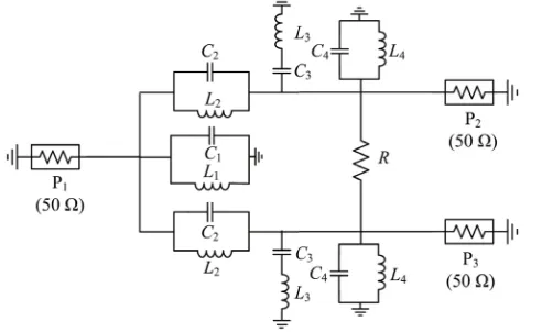
Figure 1 shows the configuration of the proposed power divider with bandpass responses. It consists of seven pairs of lumped-element capacitors and inductors as well as an isolation resistor. The capacitors and inductors can form filtering network and thus dual functions of power division and signal filtering can be realized. The circuit is modified from Wilkinson power dividers and it is symmetrical. Thus, even-and odd-mode analysis can be used to characterize it. According to the network theory of three-port symmetric network, the S-parameters can be expressed as follow [24]:
[S] = ⎡ ⎢ ⎢ ⎢ ⎢ ⎢ ⎢ ⎣
S11e
1
√
2S21e
1
√
2S21e 1
√
2S21e 1
2(S22e+S22o) 1
2(S22e−S22o) 1
√
2S21e 1
2(S22e−S22o) 1
2(S22e+S22o) ⎤ ⎥ ⎥ ⎥ ⎥ ⎥ ⎥ ⎦
(1)
whereeandocorrespond to even- and odd-mode, respectively. For ideal power dividers, the three ports are perfectly matched and ports 2 and 3 are perfectly isolated, e.g., S11 =S22=S33=S23= 0. Thus, the following conditions should be satisfied:
S11e=S22e=S22o = 0 (2)
Meanwhile,S21e should correspond to the response of a bandpass filter, so that filtering power division responses can be realized. The detailed analysis of the proposed circuit is as follows.
Figure 1. The proposed lumped-element power divider with bandpass response.
Figure 2. The odd-mode equivalent circuit.
2.1. Analysis of Odd-Mode Equivalent Circuit
Y2,o= 2
R +jωC4+ 1 jωL4
+ jωC3
1−ω2L 3C3
+jωC2+
1 jωL2
(3)
For good matching, we can get Y2,o =Yp2, whereYp2 is the characteristic admittance of port 2 and it equals to 0.02 S. Thus, we can get:
2
R =Yp2 (4)
ω(C4+C2) + ωC3 1−ω2L
3C3
= 1
ωL4
+ 1
ωL2
(5)
From Equation (4), theR is determined as 100 Ω. From the Equation (5), the operating frequency can be derived. To simplify the calculation, we define C24 = C2+C4, L24 = (L2L4)/(L2 +L4). Thus, Equation (5) can be simplified.
It is a fourth-order equation, and the operating frequencies can be deduced as
ω =±
A±√A2−4B
2 (6)
where A = 1/L3C3 + 1/L24C24+ 1/L3C24, B = 1/L3C3L24C24. There may be four roots. Two of them are negative and should be neglected. The other two positive roots correspond to two frequencies. The lower one is utilized as operating frequency ω0. The higher one is denoted as ωS. According to Equation (5) and Vieta’s theorem, we can obtain:
ω2
0+ω2S = 1/L3C3+ 1/L24C24+ 1/L3C24 (7)
ω2
0ω2S = 1/L3C3L24C24 (8)
These two equations can be used to help calculate the design parameters.
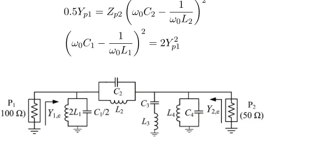
2.2. Analysis of Even-mode Equivalent Circuit
If even-mode excitation is applied to ports 2 and 3, we can get the equivalent circuit as shown in Figure 3. The impedance of port 1 becomes 2Zp1 or 100 Ω, and the capacitor and inductor close to port 1 are changed toC1/2 and 2L1. Thus, the input admittanceY1,e can be expressed as follows:
Y1,e = jωC1
2 +
1 j2ωL1
+
jωC2+ 1 jωL2
1 Zp2
+ 1
jωL4
+jωC4+ jωC3
1−ω2L 3C3
jωC2+ 1 jωL2
+ 1
Zp2
+ 1
jωL4
+jωC4+ jωC3
1−ω2L 3C3
(9)
By substituting (5) to (9), and taking into account that port 1 should be matched, we can obtain:
0.5Yp1 =Zp2 ω0C2− 1 ω0L2
2
(10)
ω0C1− 1 ω0L1
2
= 2Yp21 (11)
With these conditions, the matching of the ports can be satisfied. It does not require the 90-degree phase shift, which is necessary in some other designs [13, 17]. Meanwhile, two transmission zeros are introduced by the configuration. One is due to the parallel resonance of C2 and L2. The other transmission zero is attributed to the serial resonance of C3 and L3. The location of the two transmission zeros can be deduced as follows:
ωz1 = 2πfz1= 1
√
L2C2
(12)
ωz2 = 2πfz2= 1
√
L3C3
(13)
To improve the selectivity, the two transmission zeros are controlled to be located on the two sides of the operating band, namely, ωz1< ω0< ωz2.
Combining (10) and (12), we can calculate L2 and C2 as follows:
L2 =
√
2Zp1ω 2 0−ωz21 ω0ωz21
(14)
C2 = √ ω0
2Zp1
ω2
0−ω2z1
(15)
Combining (7), (8) and (13), the L3,C24and L24 can be determined as follows:
L3 = 1 C3ωz22
(16)
C24 = C3ω
4
z2 ω2
0ωz22+ωS2ωz22−ωz42−ω20ω2S
(17)
L24 = ω 2
0ωz22+ωS2ωz22−ωz42−ω20ω2S C3ωz22ω20ω2S
(18)
By substituting (14), (15) to (17) and (18), C4 and L4 can be calculated as follows:
C4 = C24−C2= C3ω
4
z2 ω2
0ωz22+ωS2ωz22−ωz42−ω20ω2S
−√ ω0 2Zp1
ω2
0 −ωz21
(19)
L4 =
√
2Zp1
ω2
0−ωz21 ω02ωz22+ωS2ωz22−ωz42−ω20ω2S
√
2Zp1
ω2
0 −ωz21
C3ωz22ω20ω2S−
ω2
0ωz22+ωS2ωz22−ωz42−ω20ω2S
ω0ωz21
(20)
In the above section, the issues of operating frequency, isolation and port matching have been analyzed. For a power divider with bandpass responses, the equivalent filtering circuit should be considered. For the even-mode circuit, it is equivalent to a bandpass filter consisting of lumped capacitors and inductors. The bandwidth is defined as Δf, and the 3-dB frequency points are defined asf1 =f0−Δf/2,f2=f0+ Δf/2. Therefore, the following equations should be satisfied:
S21e(L1, C3)|f=f1,f2 = 0.707 (21)
Here,S21e can be calculated by:
S21e =
1−Γ21,e (22)
Γ1,e =
0.5Yp1−Y1,e 0.5Yp1+Y1,e
(23)
3. CIRCUIT IMPLEMENTATION
Based on the design theory, we can briefly summarize the design methodology as follows. It is assumed that the circuit specificationsf0, Δf,fZ1 and fZ2 are given.
Step 1: According to the given operating frequency f0 and lower transmission zero fZ1, the parameterC2 and L2 can be determined by (14) and (15).
Step 2: Referring to the equations of (11), (16), (19) and (20), the parameters C1,L3, L4 and C4 can be represented byL1,C3 and the given upper transmission zero fZ2.
Step 3: By substitutingC1,L3,L4,C4,L1,C3,f1 and f2 to (21), we can calculated the values of L1 andC3.
Step 4: Substituting the value of L1 and C3 to (11), (16), (19) and (20), the value of C1, L3, L4 and C4 can be obtained. Thus, all values of the eight parameters have been obtained.
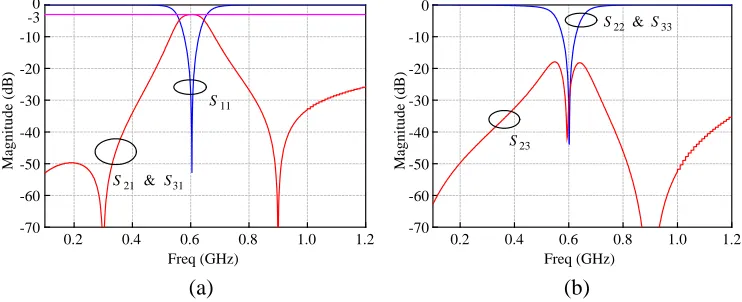
To verify the above process, a design is taken as an example. The filter specifications are given as follows: f0= 600 MHz, Δf = 100 MHz, fZ1 = 300 MHz,fZ2 = 900 MHz. Following the step 1, C2 and L2 can be calculated with the values of 5.005 pF and 56.29 nH. Then L1 and C3 can be calculated with the values of 3.064 nF and 15.95 pF in the step 3. After that, C1, L3, L4 and C4 can be obtained as follows: C1 = 15.95 pF, L3 = 1.963 nH, C4 = 2.285 pF, L4 = 2.027 nH. Thus, all the initial values are obtained. The simulation results of this ideal case are shown in Figure 4. Good power division and bandpass responses are observed. The operating frequency is located at 601 MHz and 3-dB bandwidth is 102 MHz. Two transmission zeros are located at 300 MHz and 900 MHz. The three ports are well matched. The isolation is over 40 dB at the center frequency. The good agreement between the prediction and simulation validates the analysis and design procedures.
0.2 0.4 0.6 0.8 1.0 1.2
S21 & S31 S11
0.2 0.4 0.6 0.8 1.0 1.2
S22 & S33
S23
-70 -60 -50 -40 -30 -20 -10 0
Magnitude (dB)
-3
-70 -60 -50 -40 -30 -20 -10 0
Magnitude (dB)
(a) (b)
Freq (GHz) Freq (GHz)
Figure 4. Simulated results of ideal case. (a)S11,S21 and S31. (b)S22,S33 andS23.
Figure 5. Photograph of the fabricated circuit.
0.1 0.2 0.3 0.4 0.5 0.6 0.7 0.8 0.9 1.0 Freq (GHz)
Simulated S 22
Simulated S 23
Measured S22
Measured S 33
Measured S 23
0.54 0.56 0.58 0.60 0.62
S31
-S21
(degree)
-4 -3 -2 -1 0 1 2 3 4
0.1 0.2 0.3 0.4 0.5 0.6 0.7 0.8 0.9 1.0
Smiulated S11
Simulated S21
Measured S11
Measured S21
Measured S31
(a) (b)
Measured Simulated
(c)
-50 -45 -40 -35 -30 -25 -20 -15 -10 -5 0
Magnitude (dB)
-0.8 -0.4 0.0 0.4 0.8
|S31
|-|
S21
| (dB)
-50 -40 -30 -20 -10 0
Magnitude (dB)
Freq (GHz) Freq (GHz)
Figure 6. Simulated and measured results (a)S11,S21 and S31. (b) Amplitude and phase imbalance. (c)S22,S23 and S33.
capacitors to replace the ideal ones and then conduct fine tuning. In this way, we can get the final values of practical components. The fabricated photograph is shown in Figure 5 and the total size is
15 mm×14 mm.
4. CONCLUSION
This paper has presented a novel method for designing compact power divider with bandpass responses. Both theory and experiments have been provided, showing that the filtering and power splitting circuits are highly integrated and the proposed devices can exhibit the dual functions with good performance. The closed-form design equations have been derived, which greatly simplify the design procedures. Due to the use of lumped elements, the circuit size is very compact. With these features, the proposed method is attractive for highly-integrated circuit designs in the UHF band.
ACKNOWLEDGMENT
This work was supported by the NSFC under grant Nos. 61271060 and 61271209.
REFERENCES
1. Mansour, G., M. J. Lancaster, P. S. Hall, P. Gardner, and E. Nugoolcharenlap, “Design of filtering microstrip antenna using filter synthesis approach,”Progress In Electromagnetics Research, Vol. 145, 59–67, 2014.
2. Zuo, S.-L., W.-J. Wu, and Z.-Y. Zhang, “A simple filtering-antenna with compact size for WLAN application,”Progress In Electromagnetics Research Letters, Vol. 39, 17–26, 2013.
3. Chen, X., F. Zhao, L. Yan, and W. Zhang, “A compact filtering antenna with flat gain response within the passband,”IEEE Antennas Wireless Propag. Lett., Vol. 12, 857–860, 2013.
4. Bei, L., S. Zhang, and K. Huang, “A novel dual-band multi-way power divider using coupled lines,” Progress In Electromagnetics Research C, Vol. 37, 41–51, 2013.
5. Kawai, T., H. Mizuno, I. Ohta, and A. Enokihara, “Lumped-element quadrature Wilkinson power divider,” Asia Pacific. Microw. Conf., 1012–1015, 2009.
6. Li, J. C., Y. L. Wu, Y. A. Liu, J. Y. Shen, S. L. Li, and C. P. Yu, “A generalized coupled-line dual-band Wilkinson power divider with extended ports,”Progress In Electromagnetics Research, Vol. 129, 197–214, 2012.
7. Gao, L. and X. Y. Zhang, “High selectivity dual-band bandpass filter using a quad-mode resonator with source-load coupling,” IEEE Microw. Wireless Compon. Lett., Vol. 23, 474–476, 2013. 8. Jun, S. and K. Chang, “Compact microstrip bandpass filter using miniaturized hairpin resonator,”
Progress In Electromagnetics Research Letters, Vol. 37, 65–71, 2013.
9. Singh, P. K., S. Basu, and Y.-H. Wang, “Coupled line power divider with compact size and bandpass response,”Electronics Lett., Vol. 45, 892–894, 2009.
10. Tang, X. and K. Mouthaan, “Filter integrated Wilkinson power dividers,” Microw. Opt. Tech.
Lett., Vol. 52, 2830–2833, 2010.
11. Shao, J.-Y., S.-C. Huang, and Y.-H. Pang, “Wilkinson power divider incorporating quasi-elliptic filters for improved out-of-band rejection,”Electronics Lett., Vol. 47, 1288–1289, 2011.
12. Cheong, P., K.-I. Lai, and K.-W. Tam, “Compact Wilkinson power divider with simultaneous
bandpass response and harmonic suppression,” IEEE MTT-S Int. Microwave Symp. Dig., 1588–
1591, 2010.
13. Li, Y. C., Q. Xue, and X. Y. Zhang, “Single- and dual-band power divider integrated with bandpass filters,”IEEE Trans. Microw. Theory Tech., Vol. 61, 69–76, 2013.
14. Lu, Y. L. and G. L. Dai, “Novel filtering power divider using multiple internal resistors,”Progress In Electromagnetics Research Letters, Vol. 45, 75–80, 2014.
15. Chen, C.-F., T.-Y. Huang, T. M. Shen, and R.-B. Wu, “Design of miniaturized filtering power dividers for system-in-a-package,” IEEE Trans. Component Packag. Manufact. Technol., Vol. 3, 1663–1672, 2013.
17. Deng, P.-H. and L.-C. Dai, “Unequal Wilkinson power dividers with favorable selectivity and high-isolation using coupled-line filter transformers,” IEEE Trans. Microw. Theory Tech., Vol. 60, 1520–1529, 2012.
18. Wong, S. W. and L. Zhu, “Ultra-wideband power divider with good in-band splitting and isolation performances,”IEEE Microw. Wireless Compon. Lett., Vol. 18, 518–520, 2008.
19. Xiao, L., H. Peng, and T. Yang, “Bandpass-response power divider with high isloation,” Progress In Electromagnetics Research Letters, Vol. 46, 43–48, 2014.
20. Gao, S. S., S. Sun, and S. Xiao, “A novel wideband bandpass power divider with harmonic-suppressed ring resonator,”IEEE Microw. Wireless Compon. Lett., Vol. 23, 119–121, 2013.
21. Choi, M.-G., H.-M. Lee, Y.-H. Cho, X.-G. Wang, and S.-W. Yun, “Design of Wilkinson power divider with embedded low-pass filter and cross-stub for improved stop-band characteristics,”IEEE MTT-S Int. Microwave Symp. Dig., 1–4, 2011.
22. Elsbury, M. M., P. D. Dresselhaus, N. F. Bergren, C. J. Burroughs, S. P. Benz, and Z. Popovic,
“Broadband lumped-element integrated N-way power dividers for voltage standards,” IEEE
Trans. Microw. Theory Tech., Vol. 57, 2055–2063, 2009.
23. Hou, J.-A. and Y.-H. Wang, “Design of compact 90 and 180 couplers with harmonic suppression using lumped-element bandstop resonators,” IEEE Trans. Microw. Theory Tech., Vol. 58, 2932– 2939, 2010.