Scanning Superconducting Quantum Interference
Device Microscopy
Sensitive mapping of magntic flux on thin films
Tom Wijnands
Interference Device Microscopy
By
Tom Wijnands
To obtain the degree of Master of Science,
Applied Physics
January 10
th
, 2013
Abstract
Thin films and interfaces can hold interesting phenomena. A scanning superconducting quantum interference device microscope (SSM) can map the magnetic flux of a surface. With a SSM a high magnetic resolution can be achieved. The SSM at the University of Twente has been made opera-tional again. Improving the fabrication processes and making the setup more robust. Three different materials have extensively been tested using this device. The first material is a LaAlO3/SrTiO3
interface which might have ferromagnetism and superconductivity in a single interface. This was not found in the tested samples. In the second material doped TiO2 a landscape of ferromagnetic dipoles
were found. The third material a LaMnO3 (LMO) film. The LMO films are grown on STO and are
ferromagnetic insulators. Measuring the LMO films with the SSM revealed ferromagnetic domains.
Exam committee:
Prof. Dr. Ir. H. Hilgenkamp
Dr. M.H.G. Duits
Dr. Ir. J. Flokstra P.D. Eerkes MSc Ing. D. Veldhuis
Work preformed at:
Interfaces and Correlated Electron systems group Faculty of Science and Technology
Contents
1 Introduction 1
2 Theory 3
2.1 Introduction to superconductivity . . . 3
2.2 Josphson junctions . . . 4
2.3 Flux quantization . . . 5
2.4 DC SQUID . . . 5
2.5 Flux locked loop . . . 6
2.6 Dipole Model . . . 6
3 Experimental setup 9 3.1 Equipment . . . 9
3.2 Holder . . . 11
3.2.1 Sensor . . . 12
3.2.2 Cantilever . . . 12
3.2.3 Distance . . . 14
3.2.4 Photoresist . . . 15
3.3 Software . . . 15
3.4 Signal . . . 16
3.5 Noise . . . 18
4 Results 21 4.1 Ferromagnetism at the LaAlO3/SrTiO3 interface . . . 21
4.1.1 Introduction . . . 21
4.1.2 Results . . . 22
4.2 Ferromagnetism in Ti(x-1)TaxO2(x≈0.05) . . . 23
4.2.1 Introduction . . . 23
4.2.2 Results . . . 24
4.3 Imaging of the ferromagnetic insulator LaMnO3. . . 26
4.3.1 Introduction . . . 26
4.3.2 Results . . . 26
5 Conclusions and recommendations 29
Bibliography 31
Scanning SQUID Microscopy
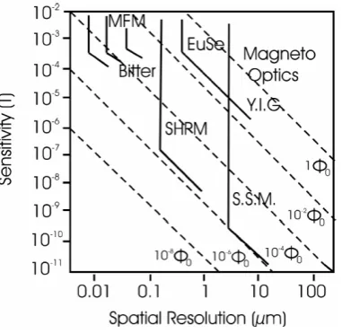
Figure 1.1: The magnetic and spatial resolutions of different magnetic microscopy techniques. This figure was published in [7].
experimental setup is explained. The changes that were made to the SSM to make it more reliable. The procedures to replace and repair the parts of the setup are also highlighted. The research that was done using this microscope is shown in chapter four. Finally in chapter five conclusions are drawn and recommendations are made.
Chapter
2
Theory
2.1 Introduction to superconductivity
Heike Kamerlingh Onnes discovered superconductivity in 1911 in Leiden. Superconductivity is one of many a quantum mechanical effects that occur in nature. In a superconductor electrons flow with zero resistance. Ohms law states that zero resistance means that superconducting materials can conduct a current without any voltage being applied. No energy dissipates during the transport process. Superconducting materials become superconducting when they are below a critical temper-ature (Tc). This temperature is material dependent and usually very low, in the order of a few Kelvin.
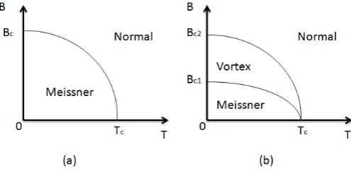
Next to the zero resistance phenomena, superconductors show another important effect. They tend to repulse all magnetic fields from the superconducting material. This effect is called the Meissner ef-fect. Magnetic fields break down the superconductivity, when a high external magnetic field is applied superconducting materials lose their superconducting effects when it is above a critical magnetic field. The breakdown can be classified into two groups. Type one superconductors lose their superconduc-tivity and behave as a normal material, when the external magnetic field is increased above a critical value (Bc), as figure 2.1 (a). In type two superconductors there is a mixed state between complete repulsion and losing the superconducting effects. In this state the magnetic field locally penetrates the superconductor creating so called Abrikosov vortices when the field strength is above Bc1, as figure 2.1 (b). The type two superconductors behave as a normal material when the field strength is above Bc2. Yttrium Barium Copper Oxide (YBCO) is an example of a type two superconductor[12].
Scanning SQUID Microscopy
I=I0sinϕ0cosπφ φ0
(2.9)
2.5 Flux locked loop
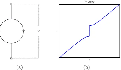
A SQUID has a non linear periodic flux to voltage conversion. The most sensitive way to operate a SQUID is using the flux locked loop (FLL) mode [21]. A schematic view of such a setup is show in figure 2.3. The SQUID operates at a constant bias current. A modulated triangular wave is applied.
One period of the applied signal corresponds roughly with one φ0. A working point is chosen by
setting the DC offset to 0 Volt.
Figure 2.3: Schematic view of a basic FFL setup. This figure was published in [22].
When the signal from the SQUID gets locked by the lock-in amplifier a working point is created. External flux that is picked up by the SQUID gives a DC offset to the working point making it a non zero value. The offset voltage is a direct measure for the external flux. With a flux locked loop operating method very low noise levels can be reached. The typical white background noise level is around a fewµφ0/√Hz.
2.6 Dipole Model
One of the common features on the scanning SQUID measurements are magnetic dipoles. To give insight on the source of these ferromagnetic effects a magnetization value should be calculated. A method to do this is to create a model for the magnetic field and fit this to the measured data [23]. The experimental situation is displayed in figure 2.4.
Here the SQUID pickup loop is above the surface of the sample and measures the magnetic field of
Figure 2.4: A schematic view of a SQUID loop at a distance from a dipole source.
a dipole at a certain distance and height from its center. The pickup loop of the SSM only picks up the out of plane magnetic fields. By fitting a model to the measured data it is possible to calculate the magnetic moment of the dipole. The magnetic field for a dipole can be derived from Biot-Savart equation. The assumption is that the dipoles consist out of two magnetic point sources.
B= µ0 4π
Z Idl×r
|r|2 (2.10)
When this is solved in three dimensions and rewritten (B=Bx+By+Bz) in Cartesian coordinates,
the equations become:
Bz,x(x, y, z)
µ0
4π3mx
xz
(x2+y2+z2)5/2 (2.11)
Bz,y(x, y, z)
µ0
4π3my
yz
(x2+y2+z2)5/2 (2.12)
Bz,z(x, y, z)
µ0
4πmz
3z2− x2+y2+z2
(x2+y2+z2)5/2 (2.13)
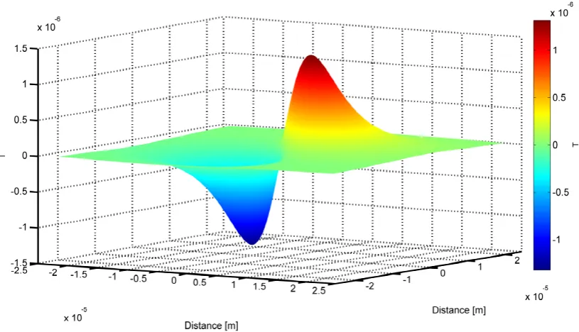
The magnetic field of a dipole as described by equations (2.11),(2.12),(2.13) can be fitted to measured SSM data. An example of a simulated dipole is displayed in figure 2.5.
Scanning SQUID Microscopy
Figure 3.1: A schematic view of the equipment used in the SSM. The black lines show how the equipment and how they are coupled together. This an updated figure version of the ICE SSM user manual.
Figure 3.2: The lever mechanism in the SSM. The SSM motors are on top and the sample at the end of the rod. This figure was published in [22].
the sensor and sample, the closer the pickup is to the sample. However if the angle is too low the wire bonds connecting the cantilever to the sensor touches the sample. The wire bonds touching the sample may damage the sample, wire bonds, or increase the noise in the measurement. The estima-tion of the distance between the center of the pickup loop and the sample issin(10◦)·(4.5+8) = 2.1µm.
3.2.4 Photoresist
A sample can be covered with a layer of photoresist. The photoresist is a thin layer of organic ma-terial roughly 1µm thick and uniformly distributed over the sample surface. The tip of the sensor moves through this layer when the sensor is in contact with the sample, see figure 3.7. If the SSM scans a sample the movement of the sensor tip on that sample causes the tip edge to be scratched off, due to the contact mode. This process is slow, but eventually the pickup loop is cut. A soft organic material might help to slow down this process making a sensor last longer. Another advantage is that it is possible to trace the scanned area. When the sensor is cooled down in the liquid helium, it is not possible to see if the sensor is on the sample, now it is possible to check this afterwards. This is especially useful if no magnetic features are measured on the sample, only noise. The alignment of the sensor to the sample changes due to shrinking of the cantilever at low temperatures. The alignment shift is usually only in the Y-direction. In rare cases the sensor can be off sample. Another advantage is that further analysis on the scanned area can be done with other surface analysis techniques like AFM or STM.
Figure 3.7: Optical image of aT iO2 sample after scanning. Patches of photoresist are removed by the scanning of the
sensor.
3.3 Software
The SSM is operated using two programs. The first is called PCS100. This program is used operate the Star Cryoelectronics PCI-100 box. With this software it is possible to make a flux locked loop. The second program is for approaching the sample and measuring the flux. This program is called npscan. Both programs are needed while scanning.
The PCS100 is an easy to use program. With tune function a modulation for the SQUID can be set if the test signal is on. Figure 3.8 displays what the modulation of the test signal looks like. The signal generator sends out a triangle wave with a frequency of 100 Hz. The output voltage should be set that the asymptote of the test signal are on the same level. As in figure 3.8. This corresponds to oneφ0. The peak to peak of the test signal should to be maximized to get an optimal flux to voltage
Chapter
4
Results
4.1 Ferromagnetism at the LaAlO
3/SrTiO
3interface
4.1.1 Introduction
In September 2011 a paper was published about the coexistence of ferromagnetism and superconduc-tivity at a LaAlO3/SrTiO3 (LAO/STO) interface. The coexistence of ferromagnetism and
supercon-ductivity is rare, because superconsupercon-ductivity breaks down with magnetism. The combination of the two materials LAO and STO is very interesting match. LAO and STO are both nonmagnetic insu-lating materials, but when together as thin films the interface between them becomes conducting. At certain growth conditions it can even be superconducting at low temperatures (300 mK). The Moler group at Stanford University uses scanning SQUID imaging on the LAO/STO interface. Using their SSM a landscape of ferromagnetism, paramagnetism and superconductivity is found. There are several possible reasons for the magnetism appear. The first is found with the help of Density functional theory(DFT). When theory is applied to a perfect interface it finds a number of nearly degenerate states. Some of these states have a spin polarization and thus gives rise to magnetism. A second possibility is the existence of oxygen vacancies at the LAO/STO interface. The oxygen vacancies make a polarized unit cell which can give rize to magnetism.[27, 28]
Figure 4.2: A typical LAO/STO SSM measurement. No magnetic features appear above the noise level.
interface as described by the papers from the Moler group in Stanford was observed. Even sample grown with the same specifications did not deliver the same results.
Figure 4.3: On the left a measured dipole and on the right the fit of the measured dipole.
4.2 Ferromagnetism in Ti
(x-1)Ta
xO
2(x
≈
0.05)
4.2.1 Introduction
In collaboration with the National University of Singapore the magnetic features of doped Titanium dioxide (T iO2) were tested. The T iO2 is grown on LaAlO3 substrate using pulsed laser deposition
(PLD). TheT iO2samples are doped with Thallium. Using normal SQUID measurements the
magne-tization peaked at a doping level around 5−6%. The measured field of theT i(x−1)T axO2(x≈0.05)
them. As can be seen in figure 4.7(a). After measuring both samples were cleaned. All the photoresist got removed. However after cleaning the dirt on the sample remained. After cleaning the samples were remeasured without photoresist. In these measurements the dipoles remained unchanged in size density and orientation.
Since the magnetic effects may occur at the interface structuring, the sample may have some effect on the dipole orientation and location. After a surface roughness scan with an AFM, the 10 nm thin film has a surface roughness of 8 nm. The 37 nm thin film has a surface roughness of 70 nm. In these films the surface roughness is equal or larger than the film thickness. A possible reason for this is that the photoresist freezes at a temperature of 4 K and while freezing it might have cracked the surface of theT iO2 films.
(a) (b)
Figure 4.7: (a) An optical image taken under a microscope displaying the sample surface of theT iO237 nm thin film.
(b) An AFM measurement of the surface of of theT iO2 37 nm thin film. The AFM scanned an area of
20x20µm.
The two thicker samples were measured with zero field cooling. However no photoresist was applied to these samples to exclude the photoresist from influencing the measurements.
Figure 4.8: A SSM measurement on a Ta dopedT iO2 350 nm film. The measurements show a landscape of dipoles.
The dipole density is higher than the thinner films (10 nm and 37 nm).
Figure 4.8 displays a measurement on the 350 nm sample. The 350 nm sample has a much higher dipole density then in the thinner films. The dipole density is here is one dipole per 50 x 50 µm2.
Scanning SQUID Microscopy
sample the 400 nm thin film no magnetic features were observed. However only one measurement was conducted. The scanned area is 0.2mm2.
With applying an external magnetic field one should be able to flip the magnetization of a dipole. However this did not happen. The maximum external field that was applied was 1 mT. Being that this external field has a weak magnetic strength it is very likely that this field too weak to make any change. Also field cooling did not change the strength, density or orientation of the dipoles. No superconducting features such as vortices were observed.
4.3 Imaging of the ferromagnetic insulator LaMnO
34.3.1 Introduction
The combination of a material being a ferromagnetic and an insulator is rare. A few ferromagnetic insulators have been discovered such asEuOandY T iO3. The working mechanisms of these materials are still under investigation. There might already be applications for these materials. Ferromagnetic insulators are good candidates for spin polarizers or for hard disk applications. In bulk LaMnO3
(LMO) is a Mott insulator, however when grown in thin film the material shows different properties. Thin films of LMO film show to have ferromagnetic properties. The precise origin of the ferromag-netism in these films is still not known. There are two possible origins for ferromagferromag-netism in these films. The first possibility is oxygen vacancies in the material and the second one is due to strain in the film. All the films were made using pulsed laser deposition of LMO on a STO(001) or 0.1% Nb doped STO (001) (NSTO) substrate.
4.3.2 Results
Two LMO samples were made using PLD, a 12 UC and a 24 UC sample. The LMO films have a resis-tance of more than one MOhm in the temperature range from 2 K to 300 K, making it an insulator. Next to general conduction across the sample also the local conduction was tested using a conducting AFM. The samples were also locally insulating. Using the SSM the surface of the sample was scanned on local magnetic properties at a temperature of 4 K. Figure 4.9 displays SSM measurements on the 12 UC and 24 UC films.
Figure 4.9: SSM measurements on different LMO samples. A 12 UC sample (left) and a 24 UC sample (right). Both measurments show ferromagnetic domains. The flux strength on the 24 UC is larger than the 12 UC sample.
The measurements show a magnetic landscape. All measurements on the LMO films show this type of landscape. The red color represents out going flux and the blue color the in going magnetic flux.
The maxima of the magnetic flux are±4mφ0. Comparing the 12 UC and 24 UC samples its shown
that the spatial size of the domains is the same. The thicker 24 UC sample shows a higher number of counts of higher flux values. The magnetic flux going in and out of the sample is higher in the 24 UC sample then in the 12 UC sample. This corresponds with the normal SQUID measurements. From this data we can conclude that de LMO is a ferromagnetic insulator.
Scanning SQUID Microscopy
on the same ferromagnetism. Of the four samples only one sample (the old 26 UC sample) contained dipoles. The total amount of four dipoles were measured. The dipole are concentrated at one loca-tion. Even the samples made with the same parameters as in Stanford did not produce the same results. The claim that our samples have ferromagnetism is not one that can be made using this data.
On the T iO2 sample a landscape of dipoles were found on the different samples. The measured
dipoles have a random orientation. The dipole density increased with the thickness of the film. No domains and vortices were observed in these films. The last material that was investigated is LMO. On LMO ferromagnetic domains were found across the whole sample. The flux on the surface of a sample increases with film thickness. LMO is an insulating material. This makes LMO a ferromag-netic insulator.
Bibliography
[1] Binnig, G., Quate, C. F., and Gerber, C. (1986)Physical Review Letters56, 930.
[2] Binnig, G., Rohrer, H., Gerber, C., and Weibel, E. (1982)Physical Review Letters49(1), 59.
[3] Jaklevic, R. C., Lambe, J., Silver, A. H., and Mercereau, J. E. (1964)Advances in Physics12(7), 159.
[4] Vu, L. N. and Harlingen, D. J. V. (1993)IEEE Transactions on Applied Superconductivity3(1), 1918.
[5] Davidy, B., Grundlerz, D., Kreyz, S., Doormanny, V., Eckarty, R., Krummey, J. P., Rabey, G., and Doessely, O. (1996)Superconductor Science and Technology9, 4A.
[6] Kirtley, J. R., Tsuei, C. C., Moler, K. A., Kogan, V. G., Clem, J. R., and Turberfield, A. J. (1999)Applied Physics Letters74(26), 4011.
[7] Kirtley, J. R., Ketchen, M. B., Tsuei, C. C., Sun, J. Z., Gallagher, W. J., Yu-Jahnes, L. S., Gupta, A., Stawiasz, K. G., and Wind, S. J. (1999)Advances in Physics48(4), 449.
[8] Sandhu, A., Kurosawa, K., Dede, M., and Oral, A. (2004) Japanese Journal of Applied Physics
43, 777.
[9] Kirtley, J. (2002) Physica C368, 55.
[10] Huber, M. E., Koshnick, N. C., Bluhm, H., Archuleta, L. J., Azua, T., Bjornsson, P. G., Gardner, B. W., Halloran, S. T., Lucero, E. A., and Moler, K. A. (2008)Review of Scientific Instruments 79(5), 053704.
[11] Kirtley, J. and Wikswo, J. P. (1999)Annual Review of Materials Research29, 117.
[12] Wu, M. K., Ashburn, J. R., Torng, C. J., Hor, P. H., Meng, R. L., Gao, L., Huang, Z. J., Wang, Y. Q., and Chu, C. W. (1987)Physical Review Letters58(9), 908.
[13] Bardeen, J., Cooper, L. N., and Schrieffer, J. R. (1957)Physical Review108, 1175.
[14] Yun, S. H. and Wua, J. Z. (1996)Applied Physics Letters68(6), 862.
[15] Josephson, B. D. (1962)Physics Letters1(7), 251.
[16] Jansman, A. B. M. High-Tc dc SQUIDs for use in a background field PhD thesis University of Twente (1999).
[17] Cyrot, M. and Pavuna, D. (1992) Introduction to superconductivity and high-Tc materials, World Scientific Pub Co Inc, .
Scanning SQUID Microscopy
[19] McCumber, D. (1968) Journal of Applied Physics39, 3113.
[20] Clakre, J. and Braginski, A. (2004) The SQUID Handbook: Vol.1 Fundamentals and Technology of SQUIDs and SQUID Systems, Wiley-VCH, first edition.
[21] Koch, R. H., Rozen, J. R., Woltgens, P., Picunko, T., Goss, W. J., Gambrel, D., Lathrop, D., Wiegert, R., and Overway, D. (1996)Review of Scientific Instruments67(8), 2968.
[22] Troeman, A. G. P. NanoSQUID Magnetometers and High Resolution Scanning SQUID Mi-croscopy PhD thesis University of Twente (2007).
[23] Adamo, M. Nappi, C. and Sarnelli, E. (2008) Measurement Science and Technology 19(1),
015508.
[24] Verwijs, C. J. M. Fractional flux quanta in high-Tc/low-Tc superconducting structures PhD thesis University of Twente (2009).
[25] Lee, J. and Lemberger, T. R. (1993)Physical Review Letters62(19), 2419.
[26] Kirtley, J. R., Ketchen, M., Stawiasz, K. G., Sun, J. Z., Gallagher, W. J., Blanton, S. H., and Wind, S. J. (1995)Applied Physics Letters66(9), 1138.
[27] Bert, J. A., Kalisky, B., Bell, C., Kim, M., Hikita, Y., Hwang, H. Y., and Moler, K. A. (2011) Nature Physics7(10), 767.
[28] Kalisky, B., Bert, J. A., Klopfer, B. B., Bell, C., Sato, H. K., Hosoda, M., Hikita, Y., Hwang,
H. Y., and Moler, K. A. (2012)Nature Communications3(922), 1931.
[29] Rusydi, A., Dhar, S., Barman, A. R., Ariando, Qi, D., Motapothula, M., Yi, J. B., Santoso, I., Feng, Y. P., Yang, K., Dai, Y., Yakolev, N. L., Ding, J., Wee, A. T. S., Neuber, G., Breese, M.
B. H., Ruebhausen, M., Hilgenkamp, H., and Venkatesan, T. (2012)Philosophical Transactions
of the Royal Society A370(1977), 4927.
[30] Hayashi, M., Kaiwa, T., Ebisawa, H., Matsushima, Y., Shimizu, M., Satoh, K., Yotsuya, T., and Ishida, T. (2008)Physica C468, 801.
Chapter
6
Acknowledgments
In the final page of my report i would like to thank everyone who I worked with these past ten months. I really enjoyed my time at ICE working on this project. I want to thank Hans for his enthusiasm and suggestions. I also want to thank Michiel Duits for taking part in my Graduation commission. And Jaap for solving some last minute problems.
![Figure 2.3: Schematic view of a basic FFL setup. This figure was published in [22].](https://thumb-us.123doks.com/thumbv2/123dok_us/1054517.1131793/12.595.249.380.598.722/figure-schematic-view-basic-ffl-setup-gure-published.webp)