ISSN (Print) : 2320 – 3765 ISSN (Online): 2278 – 8875
I
nternational
J
ournal of
A
dvanced
R
esearch in
E
lectrical,
E
lectronics and
I
nstrumentation
E
ngineering
(An ISO 3297: 2007 Certified Organization)
Vol. 5, Issue 4, April 2016
Wide Range of Voltage Conversion Using
Level Shifter with Sleep Transistor In
Multisupply Voltage Design
S.Devaponsutha¹, A.S.Narmadaa²
PG Student [VLSI Design], Dept. of ECE, Madha Engineering College, Chennai, Tamilnadu, India ¹
Assistant Professor, Dept. of ECE, Madha Engineering College, Chennai, Tamilnadu, India ²
ABSTRACT: Multisupply voltage design using Level Shifter based on Multithreshold CMOS technique is an effective approach to reduce power.Multisupply voltage design technique is widely used in modern system-on-chips to tradeoff energy and speed. Level shifters (LSs) allow different voltage domains to be interfaced. In this brief, new LS is presented for fast and wide range voltage conversion. Because ofa novel architecture combined with the use of multithreshold CMOStechnique, the proposed circuit guarantees robust voltage shifting, which exhibits fastresponse and low energy consumption. Level Shifter is combined with Sleep transistor for reducing the power. When implemented in a 90-nmtechnology node, theproposed design reliably converts 100-mV input signals into 1 V output
signals. Post-layout simulation results demonstrate that this new LS shows a power output as 7.56x10-008W and Level
Shifter along with Sleep transistor provide the power output as 8.79x10-010W.
KEYWORDS:Level Shifter, Multithreshold CMOS, Sleep transistor, Multisupply voltage design(MSVD).
I.INTRODUCTION
A number of techniques can be used to provide large voltage conversion range in modern system-on-chip applications. Fast and wide range voltage conversion in multi supply voltage is used for reducing power, increasing speed and to obtain large voltage conversion range. Supply voltage is one of the dominant factors that determine the timing performance and power consumption of VLSI chips. Multisupply voltage domain (MSVD) technique is emerging as an effective method to reduce both dynamic and leakage powers intoday’s system-on-chips [1]. This approach consists of partitioning the design into separate voltage domains (or voltage islands), each operating at a proper power supply voltage level depending on its timing requirements. Time critical domains run at higher power supply voltage (VDDH) to maximize the performance, whereas noncritical sections work at lower power supply voltage (VDDL) to improve power efficiency without impacting on the overall circuit performance.
ISSN (Print) : 2320 – 3765 ISSN (Online): 2278 – 8875
I
nternational
J
ournal of
A
dvanced
R
esearch in
E
lectrical,
E
lectronics and
I
nstrumentation
E
ngineering
(An ISO 3297: 2007 Certified Organization)
Vol. 5, Issue 4, April 2016
which exhibits very low static and dynamic energy consumption [10]. This is obtained at the expense of reduced voltage conversion range, and of relatively limited speed. In this brief, we present a new LS that trades a certain amount of static power for a significantly improved operating speed and an extended voltage conversion range. When implemented with the 90-nm CMOS technology, the new design reliably converts input signals as low as 0.1 V to the 1 V voltages.
II. PROPOSED SYSTEM
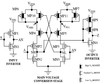
The proposed system architecture consists of three stages they are input inverter stage, main voltage conversion stage and output inverter stage. In the proposed architecture each transistors perform its own function. The MTCMOS
technique uses two type transistors in this design to provide fast switching and better performances. Logic is supplied
by a virtual power rail. Low Vth devices are used in the logic where fast switching speed is important. High Vth devices
connecting the power rails and virtual power rails are turned on in active mode, off in sleep mode. High Vth devices are
used as sleep transistors to reduce static leakage power.
The system architecture is shown in Fig 1.1
Fig 1.1 Proposed System Architecture
ISSN (Print) : 2320 – 3765 ISSN (Online): 2278 – 8875
I
nternational
J
ournal of
A
dvanced
R
esearch in
E
lectrical,
E
lectronics and
I
nstrumentation
E
ngineering
(An ISO 3297: 2007 Certified Organization)
Vol. 5, Issue 4, April 2016
TABLE 1.1 Purpose of Each Transistor
TRANSISTOR TYPE PURPOSE
MP1,MN1 Lvt Fast differential low voltage input
signal
MN2,MN3 Lvt Provide higher strength of
pull-down network for main
conversion range.
MP2,MP3 Lvt Limits cross bar current
MP4,MP5 Hvt Helps in weakening the pull-up
networks and reduce leakage current flowing through the pull-up networks when they are turned off.
MP6,MP7 Hvt Diode connected transistor for
reliable voltage conversion.
MP6-MP10,MP7-MP11 Hvt Diode connected transistors to
reduce switching delay
MP10,MP11 Hvt Controlled by NH and NL node
MN4 Svt Allows static current
MP9,MP8 Stacked HvtPMOS Control the static current
discharge in MN4 ,when NH is
high to significantly reduced.
.
III. DATA FLOW DIAGRAM
INPUT INVERTER
MAIN VOLTAGE CONVERSION STAGE
OUTPUT INVERTING BUFFER
ISSN (Print) : 2320 – 3765 ISSN (Online): 2278 – 8875
I
nternational
J
ournal of
A
dvanced
R
esearch in
E
lectrical,
E
lectronics and
I
nstrumentation
E
ngineering
(An ISO 3297: 2007 Certified Organization)
Vol. 5, Issue 4, April 2016
IV MODULE DESCRIPTION
The proposed system has three modules they are
Input inverter stage
Main voltage conversion stage
Output inverter stage
4.1 Input inverter stage
Two transistor have been used at the input inverter stage (MP1/MN1).The input provided will be “A”. The inverted outputs obtained by this “AN”.MP1/MN1 transistor are the low threshold transistor, used for fast differential low-voltage input signal to Main low-voltage conversion range.
4.2Main voltage conversion range
Main voltage conversion range used as LS to shift voltage from one domain to another. Before the rising (falling) transition of the input signal A (AN), the nodes NH and NL are held high and low, respectively. Therefore, MP10 is switched off and MP11 is switched on. A high to low transition of the main input causes MP4 being turned on. Its drain
current brings the diode-connected MP6, MP10device into the saturation region. This creates a voltage drop (i.e., Vth,
MP6, MP10) across MP6, MP10terminals that produces a correspondent bulksource voltage drop on MP4. Due to the
bulk effect, this increases the MP4 threshold voltage. The reduced voltage level (VDDH-Vth, MP6, MP10) on the
source terminal of MP4 limits its VGS, thus further weakening the MP4 action. All the above effects reduce the contention on the node NH, thus allowing faster discharging to be achieved. When MP4 is turned on, MP5 is consequently turned off.
In this case, the small leakage current flowing through MP5 is not enough to turn MP7 on. For this reason, MP5 results power gated from the VDDH power rail, leading to a significant reduction in its sub-threshold current. The diode-connected MP7 device participates in minimizing the leakage current, also by increasing the threshold voltage of MP5. In fact, MP7get full VDDH voltage. As the input signal switches, the transistor MN2 is turned on and the node NH starts to be discharged. Owing to this, MP4 is weakened, thus speeding up the discharge of the node NH. In the meantime, the stronger pull-up of the right branch charges the node NL and a positive feedback is triggered causing MP4 to be turned off. This allows the discharging of NH to be further accelerated. As NH approaches the ground voltage, the positive feedback is again triggered, causing MP5 to be completely turned on. Therefore, NL is fully charged at the VNLL voltage level. Once transitions on the nodes NH and NL are completed, the virtual power supplies
VNHH = VDDH and VNLL = VDDH−Vdsat, MP7 are establishedto provide fast switching in the subsequent input
transition.
4.3 Output inverter stage:
The output inverter stage is designed using standard threshold voltage transistor and stacked high threshold voltage transistors. These transistors get the output signal Z from the main voltage conversion stage. The extra PMOS
transistor in the output inverter is used to control the static discharge of MP8 transistors by maintaining the source gate
voltage below VDDH.From this Vt of MP8 increases. So the source gate voltage of MP8 decreases.So,it reduce static current.
As this moment, sleep transistor is placed in series with MP6-MP10, MP7-MP11, MP8 and power supply. The sleep control scheme is used for efficient power supervision.In active time,sleep transistor is turned ON,while their on-resistances issmall and supply voltage almost function as real power line.During standby manner,sleep transistor turned off and decreasing the power dissipation.
V. RESULT
ISSN (Print) : 2320 – 3765 ISSN (Online): 2278 – 8875
I
nternational
J
ournal of
A
dvanced
R
esearch in
E
lectrical,
E
lectronics and
I
nstrumentation
E
ngineering
(An ISO 3297: 2007 Certified Organization)
Vol. 5, Issue 4, April 2016
Table 5.1 Resource Comparison for Power in existing method
CONFIGURATION TECHNOLOGY (nm) DELAY (ns) POWER(µW)
CVS 90 28.27 -
DCVS 90 25 17.6
Current mirror 130 18.5 20.4
Table 5.2 shows that the power in proposed system of Multi-threshold CMOS technology and Multi-threshold CMOS technology along with Sleep Transistor.
Table 5.2 Resource for power in proposed system
CONFIGURATION TECHNOLOGY (nm) POWER(W)
MT-CMOS 90 7.568217e-008
MT-CMOS with Sleep transistor 90 8.796456e-010
This type of configurations is now used in modern system on chip to trade off power and speed. These low power circuits can be used to provide both low and high supply voltages with minimum power. Here by simulation can obtain a large voltage conversion range can be obtained by some 100mv to 1v this process of switching takes place with minimum delay. The power of the circuit can be varied by changing the channel length of each transistor the length and width for each device is already set to default in the tool for all types of transistors.
Here the virtual power supplies are varied in accordance with the input signal A. the two nodes follow the
rising and falling transition of the device. If the node NH is weak the virtual power supply VNNH can be fed with
voltage VDDH-VDsat the VDsat is the voltage just below the switching voltage. If the node NL is strong the node VNNH is
supplied with the full voltage VDDH ie, 1V.
The fig 5.1.a shows the schematic of Level shifter of multi-threshold CMOStechnology.
Fig 5.1.aSchematic Diagram of Level Shifter
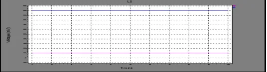
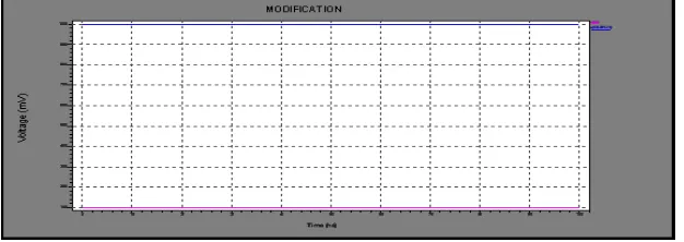
The fig 5.1.b shows the output waveform of level shifter with input A and Output Z.While giving 100mv as the input it produce the output as 1V.
ISSN (Print) : 2320 – 3765 ISSN (Online): 2278 – 8875
I
nternational
J
ournal of
A
dvanced
R
esearch in
E
lectrical,
E
lectronics and
I
nstrumentation
E
ngineering
(An ISO 3297: 2007 Certified Organization)
Vol. 5, Issue 4, April 2016
The power results of level shifter are given below
Power Results
VDD GND from time 0 to 1e-007
Average power consumed -> 7.568217e-008 watts Max power 7.568217e-008 at time 8e-008 Min power 7.568217e-008 at time 4e-008
The fig5.2.a shows the schematic waveform of level shifter with sleep transistor in Multi-threshold transistor.
Fig 5.2.aSchematic Diagram of level shifter with sleep transistor
The fig 5.2.b shows the output waveform of level shifter with sleep transistor with input A and output Z. While giving 100mv as the input it produce the output as 1V.
Fig 5.2b Output Waveform of level shifter with sleep transistor
The power results of level shifter with sleep transistor are given below
Power Results
VDD GND from time 0 to 1e-007
Average power consumed -> 8.796456e-010 watts Max power 9.246118e-008 at time 6.1e-008 Min power 1.001646e-009 at time 6e-008
VI. CONCLUSION AND FUTURE WORK
The proposed architecture exploits proper design strategies to increase the operating speed while maintaining very low energy consumption and large voltage conversion range. A new level shifter allows multi supply voltage conversion which uses CMOS technique. Such circuit guarantees robust voltage shifting from the deep sub threshold to the above threshold while exhibiting fast response and low energy consumption.
ISSN (Print) : 2320 – 3765 ISSN (Online): 2278 – 8875
I
nternational
J
ournal of
A
dvanced
R
esearch in
E
lectrical,
E
lectronics and
I
nstrumentation
E
ngineering
(An ISO 3297: 2007 Certified Organization)
Vol. 5, Issue 4, April 2016
REFERENCES
[1].Chi J. C., Lee H. H., Tsai S. H., and Chi M. C., “Gate level multiple supply voltage assignment algorithm for power optimization under timing constraint,” IEEE Trans. Very Large Scale Integr. (VLSI) Syst., vol. 15, no. 6, pp. 637–648, Jun. 2007.
[2].Clark L., Deutscher N., Demmons S., and Ricci F., “Standby power management for a 0.18 μm microprocessor,” in Proc. Int. Symp. Low Power Electron.Des., Aug. 2002, pp. 7–12 .
[3]. Ishihara F., Sheikh F., and Nikolic B., “Level conversion for dual-supply systems,” IEEE Trans. Very Large Scale Integr. (VLSI) Syst., vol. 12, no. 2, pp. 185–195, Feb. 2004.[
4]. Koo K.-H.,.Seo J.-H,.Ko M.-L, and Kim J.-W., “A new level-up shifter for high speed and wide range interface in ultra deep sub-micron,” in Proc. IEEE Int. Symp. Circuits Syst., May 2005, pp. 1063–1065.
[5].Lanuzza M., Corsonello P., and Perri S., “Low-power level shifter for multi-supply voltage designs,” IEEE Trans. Circuits Syst., Exp. Briefs, vol. 59, no. 12, pp. 922–926, Dec. 2012.
[6]. Lin Y.-S. and Sylvester D. M., “Single stage static level shifter design for subthreshold to I/O voltage conversion,” in Proc. 13th ISLPED, Aug. 2008, pp. 197–200.
[7].LütkemeierS.andRückert U., “A subthreshold to above-threshold level shifter comprising a wilson current mirror,” IEEE Trans. Circuits Syst.,
Exp. Briefs, vol. 57, no. 9, pp. 721–724, Sep. 2010. [8].Marco Lanuzza,PasqualeCorsonello and StefaniaPerri.,”Fast and wide range voltage conversion in Multisupply Voltage Design”IEEE Trans. On
VLSI systems,Vol 23,No.2,Feb 2015.
[9]. Osaki Y., Hirose T., Kuroki N., and Numa M., “A low-power level shifter with logic error correction circuit for extremely low-voltage digital CMOS LSIs,” IEEE J. Solid-State Circuits, vol. 47, no. 2, pp. 1776–1783, Jul. 2012.
[10].Wooters S. N., Calhoun B. H., and Blalock T. N., “An energy-efficient subthreshold level converter in 130-nm CMOS,” IEEE Trans. Circuits Syst., Exp. Briefs, vol. 57, no. 4, pp. 570–578, Apr. 2010 . [11] .Zhaiet al B.., “Energy-efficient subthreshold processor design,” IEEE Trans. Very Large Scale Integr. (VLSI) Syst., vol. 17, no. 8, pp. 1127– 1137, Aug. 2009.
BIOGRAPHY
Miss.S.Devaponsutha received the B.E degree in Electronics and Communication Engineering in 2014 from Mar Ephraem College of Engg &Tech/Anna University, Chennai. She is currently doing PG VLSI Design in 2016 at Madha Engineering College at Anna University, Chennai. Her Research activities based on Fast and wide range of voltage conversion in multi supply voltage used for reduction of power, increase speed and to obtain large voltage conversion range.