Voltage Gain Comparison of Z-Source
Multilevel Inverter with Different Boosting
Techniques
B.M.Manjunath
1, J.Nagarjuna Reddy
2, M.Sreedevi
3Assistant professor, Dept. of EEE, RGM Engineering College, Nandyal Andhrapradesh, India1 Assistant professor, Dept. of EEE, RGM Engineering College, Nandyal Andhrapradesh, India2 PG Student [PE], Dept. of EEE, RGM Engineering College, Nandyal, Andhrapradesh, India3
ABSTRACT: This paper proposes Z- source network is connected to multilevel inverter to obtained high voltage gain with reduced THD and voltage stress; here PV cell will act as a DC source. Now a day‟s multilevel inverter gives more improvement in AC transmission systems, power quality devices, etc. Normally carrier based PWM techniques are used in conventional inverter, but boost operation is not possible, Z- source network is used to get high voltage gain and reliability. By using different boosting techniques i.e., Simple boost, maximum boost & maximum constant boost gating pulses are generated. The performance of five level diode clamped z-source multilevel inverter has been analyzed. The simulation of five level diode clamped z-source multilevel inverter developed by using MATLAB/SIMULINK
KEYWORDS: Boost technique, multilevel inverter, PV cell, Voltage gain, Z-source network.
I.INTRODUCTION
Now a day‟s energy is essential in every one‟s life, this is especially true in this new century. Different types of energy sources are used to generate electricity, Energy sources are classified into two types, first one is renewable energy sources, second one is non renewable energy sources. In case of non- renewable energy sources (coal, oil ,gas) cannot regenerate electricity after utilization and also produces waste disposal into environment, But renewable sources (fuel cell, PV cell, wind energy) take important role in society for electrical energy generation due to regeneration of electricity after utilization of sources, pollution free, no fuel cost. Hence PV cell is taken as voltage source. The existing converters are voltage source inverter and current source inverter. In voltage source converter and current source have some disadvantages i.e. the output voltage is limited and cannot be exceed, suppose we want to increase output voltage we require additional equipment, two switches are on at time there is short circuit occurred, switches are damaged.
In current source inverter voltage cannot be exceed and also to obtained high voltage than compare to input voltage by using additional equipment ,two switches are off at time there is open circuit is occurred, switching devices are damaged. These disadvantages are rectified by using Z-source inverter as shown in fig 1.Z-Source network is connected between PV cell and main circuit to boost voltage, reduced THD, increases reliability, equivalent circuit of Z-source inverter is shown in fig.1 .It consists of two inductors and two capacitors to reduce ripple content in output wave forms. Multilevel inverter is used because it provides so many features i.e. to obtain high voltage, high power, voltage stress is reduced and harmonic content is reduced. This paper consists of five units, II Unit clearly explained about Z-source inverter, Boosting techniques in Unit III, multilevel inverter in Unit IV, simulation results in Unit V, and conclusion in Unit VI.
II.Z-SOURCE INVERTER
also cost increased[1]. Suppose two switches on in one phase leg / in two phase legs / three phase legs then short circuit occur to get dead time interval, in another case also there are two switches off in one phase leg/two phase legs /three phase legs, here get over lapping period, during these periods switching devices are damaged. There is no protection circuit, Electromagnetic interference (EMI) noise in conventional inverter. Conventional inverter do not have unique features i.e. voltage source inverter acts as only buck inverter in DC to AC power conversion, current source inverter acts as only boost inverter in DC power to AC power conversion.
Z-source inverter consists of impedance network to get boost output voltage, It also have unique features i.e. AC to AC power conversion ,DC to DC power conversion, DC to AC power conversion, AC power to DC power conversion.
Fig.1 Equivalent circuit of Z-source inverter
It consists of two inductors and two capacitors to create impedance network, the function of inductors is to reduce current ripples and increase the non shoot through state voltage, the role of capacitor is to reduce the current ripples and to ensure a soft dc voltage at inverter input. Z-source inverter equivalent circuit as shown in figure1.
Impedance network acts like second order filter, is used to buck or boost input voltage and also improve the power factor, reduce harmonics, common mode voltage ,low inrush current. There is no additional equipment between source and load, so there is no additional loss.
2A.OPERATING PRINCIPLE OF Z-SOURCE INVERTER
It consists of two modes of operation
Mode 1: During this mode of operation diode is conducting; energy is stored in inductors and capacitors. It is as active state in Z-source inverter shown in figure 2; in this state harmonics are reduced. It consists of six active states.
Fig.2 Equivalent circuit of Z-source inverter during active state.
Fig.3 Equivalent circuit of Z-source inverter under shoot-through state
2B. CIRCUIT ANALYSIS
Assume the inductors (L1&L2) and capacitors (C1&C2) have the same inductance and capacitance values respectively. From the above equivalent circuit during shoot through state
VC1=VC2= VC (1)
VL1=VL2=VL
VL=VC, Vd=2VC, Vi=0 (2)
Where, Vc is a capacitor voltage, VL is a inductor voltage,
During active state
VL=V0-VC (3)
Vd=V0, Vi= Vc-VL*VC -(V0-VC) (4)
Vi=2VC-VO (5)
Where, V0 is the dc source voltage and T=T0+T1,
D0=shoot through duty ratio, T0=shoot through state time period ,T1=active state time period
The average voltage of the inductors over one switching period (T) should be Zero in steady state. VL=T0*VC+T1*(V0-VC)/T =0
VL=(T0*VC+T1V0-VC T1)/T=0
VL=(T0-TC)-VC/T+(T1+V0)/T
VC/V0=T1/T1-T0 (6)
Similarly the average dc link voltage across the inverter bridge can be found as follows. From equation 4
VI=VI= (T0*0+T1*(2VC-V0))/T
VI= (2Vc.T1/T)-(T1.V0/T)
2VC=V0
From equation 6
T1.V0/( T1-T0)=2Vc. T1/( T1-T0)
VC=VO*T1/(T1-T0)
The peak DC link voltage across the inverter bridge is Vi= Vc-Vi=2Vc-V0
=T/(T1-T0)*Vo=B.V0 (7)
Where
B=T/ T1-T0 (8)
B is the boost factor
The output peak phase voltage from the inverter is
Vac =M.Vi/2 (9)
Where M is the modulation index in this source
Vac=M.B.V0/2 (10)
T= total switching interval, Vc=capacitor voltage, Output voltage can be stepped up and down by gain
Gain =M.B (11)
III. BOOSTING TECHNIQUES
These are used to generate pulses for switching devices. Normally carried based PWM method is used in conventional inverter there is no voltage boost but in Z-source inverter shoot through state is introduced to get boost in output voltage by insert two constant values or envelopes [2]. The boosting techniques are (a) Simple boost Pulse Width Modulation method, (b) Maximum boost pulse width Modulation method and (c) Maximum Constant Boost pulse width modulation method.
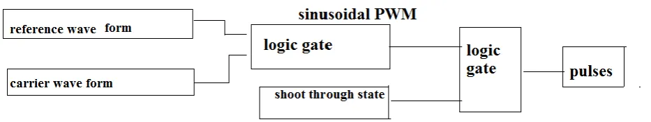
Block diagram for pulse generation
Fig .4.Block diagram for pulse generation
In Fig .4 shows comparing reference wave form with carrier wave form (triangular wave form) we obtained sinusoidal pulse width modulation, this one is combined with shoot though state then we get pulses for switches which are used in main circuit. Shoot-through state is obtained when triangular wave compare with constant or envelope.
3A. SIMPLE BOOST CONTROL METHOD
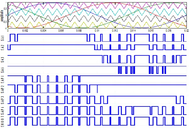
It is a straight forward method, uncomplicated method. Figure 5 illustrates the simple boost control PWM. Here a straight line is equal to or greater than or lower than the peak values of reference wave forms to control the shoot through duty ratio[1][2]. All zero states are not utilized; duty ratio is limited to (1-M), M=modulation index. Whenever modulation index=1 no boost in voltage gain. Shoot –through state is inserting in sinusoidal PWM (as shown in fig 5) to obtained boost voltage. In simple boost produced output voltage with high gain, smaller modulation index, due to this obtained high voltage stress across switching devices as shown in fig 5. In this method voltage stress is high, it limits high voltage gain and also voltage rating of devices. These limitations are rectified by using maximum boost control method.
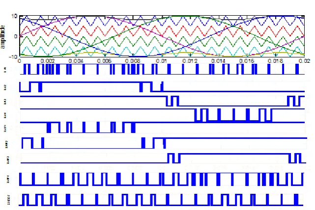
3B.MAXIMUM BOOST CONTROL METHOD
In this method reducing voltage stress under a desired voltage gain becomes more important to control Z-source inverter [5]. All traditional zero states are converted to shoot through states, due to conversion minimize the voltage stress across the devices. This control method introduces low current ripples in inductor current and capacitor voltage, it gives high voltage gain and high modulation index as shown in fig 6. Maximum boost control method PWM, the shoot through interval state repeats periodically every 𝜋
3 as shown in below fig 6.
3C.MAXIMUM CONSTANT BOOST CONTROL TECHNIQUE
This method consists of five modulating wave forms i.e. three reference waves (𝑉𝑎,𝑉𝑏, 𝑉𝑐), two envelope wave forms
(𝑉𝑝, 𝑉𝑛).Shoot through state duty ratio is obtained when carrier triangular wave is greater than the upper envelope or
lower than the lower envelopes shown in figure 7.By using this method to reduced the volume and cost of Z-source network, we need to eliminate the low frequency current ripples with constant duty ratio [7]. Here we get maximum boost factor at given modulation index and also voltage stress across the switches is reduced.
To get better results from constant boost control method than above two methods, and Modulation index and boost factor are increased and also high voltage gain voltage stress reduced not less than the maximum boost voltage.
Fig.5 Simple boost control method pulse width modulation for one leg
Fig 7 .maximum constant boost pulse width modulation for one leg
TABLE-II Summary of Different Pulse width modulation Techniques of Z-source inverter
Control methods
Simple boost Maximum boost Maximum Constant boost Duty ratio(D0 1-M 2𝜋 − 3√3𝑀
2𝜋
2 − √3𝑀 2
Boost factor(B) 1
2𝑀 − 1
𝜋 (3√3𝑀 − 𝜋)
1 (√3𝑀 − 1)
Gain(G) 𝑀
2 𝑀 − 1
𝜋𝑀 3√3𝑀 − 𝜋
𝑀
√3𝑀 − 1
Modulation index (M) 𝐺
2 𝐺 − 1
𝜋𝐺 3√3𝐺 − 𝜋
𝐺
√3𝐺 − 1
Voltage Stress(Vi)
(2G-1)V0
3√3𝐺−𝜋
𝜋 V0 (√3G-1)V
0
In table –II describes summary of different pulse width modulation of z-source inverter, gives relation between duty ratio, gain, boost factor, voltage stress in terms of modulation index (M).
IV-MULTILEVEL INVERTER
In numerous applications requires high voltage gain, high power with reduced THD, voltage stress reduced with increment of levels.
Different topologies of multilevel inverter are (1) Diode clamped multilevel inverter (2)Flying capacitor multilevel inverter (3)Cascaded multi level inverter.
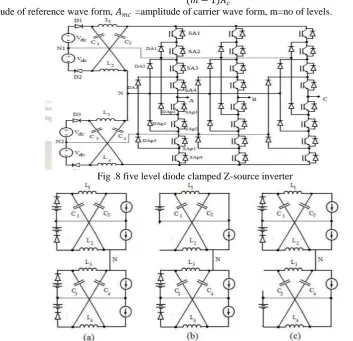
4.1 DIODE CLAMPED MULTILEVEL INVERTER
Diode clamped Multilevel inverter consists of (m-1) capacitors on DC bus produces m levels on the phase voltage .Figure shows one leg of a Five level Diode clamped Multilevel inverter the numbering order of switches SA1, SA2, SA3, SA4, S𝐴𝑝1, S𝐴𝑝2,S𝐴𝑝3, S𝐴𝑝4as shown in figure 8.Series connected capacitors are used to divide dc voltage into
equal number of dc sources[12][13]. Clamping diodes are useful to reduce the voltage stress across the switches. Each switching device block the voltage is 𝑉0
𝑚 −1,where m=no of levels 𝑉0= 𝑑𝑐 𝑣𝑜𝑙𝑡𝑎𝑔𝑒,capacitor blocks voltage is 𝑉0
𝑚 −1.
Switching table for one leg of Z-source Five level Diode clamped is given in TABLE-II.
Figure 9 represents upper shoot-through state and lower shoot-through state of five level diode clamped Z-source inverter. Multicarrier based PWM strategy is used in multilevel inverter, it is similar to sinusoidal pulse width modulation, and here number of triangular (carriers) is compared with sinusoidal wave form. In this no of carriers are needed to produce output voltage like „m‟ level of carriers are produce output is (m-1).Modulation index is defined as
𝑚𝑎=
2𝐴𝑚
(𝑚 − 1)𝐴𝑐
𝐴𝑚=amplitude of reference wave form, 𝐴𝑚𝑐 =amplitude of carrier wave form, m=no of levels.
Fig .8 five level diode clamped Z-source inverter
TABLE-III switching table for one leg of Diode clamped multilevel inverter
VA0 SWITCHING TABLE
SA1 SA2 SA3 SA4 SAP1 SAP2 SAP3 SAP4
V1=0 0 0 0 0 1 1 1 1 V2=VDC/4 0 0 0 1 1 1 1 0 V3=VDC/2 0 0 1 1 1 1 0 0 V4=3VDC/4 0 1 1 1 1 0 0 0
V5=VDC 1 1 1 1 0 0 0 0
Table –III describes switching devices operation in diode clamped multilevel inverter, upper switches (SA1,SA2,SA3,SA4) are turned off and lower devices (SAP1,SAP2,SAP3,SAP4)are turned on (0 means turned off,1
means turned on)then output voltage is zero. when lower devices are turnoff and upper devices are turn on output voltage is dc voltage VDC.
V-SIMULATION RESULTS
Simulation parameters are given as follows inductance and capacitances are 𝐿1= 𝐿2= 3.3𝑚𝐻, 𝐶1= 𝐶2= 5𝑚𝐹.Input
voltage is 400v,sw itching frequency is 10000Hz ,load is R- load R=5 ohms.
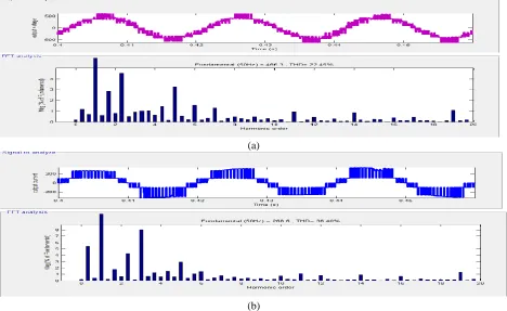
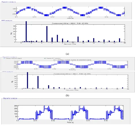
Z-source diode clamped multilevel inverter was modelled in simulink, Figure 10 shows the FFT plot for the output voltage ,output current and voltage stress in simple boost control output line voltage is 466V, output current is 266.6amps for five level at modulation index=0.8. Here input voltage is obtained from PV cell (400 V). Figure 11 shows FFT plot for the output voltage output current and voltage stress in maximum boost control output line voltage is 668.6V, output current is 383.7amps for five level at modulation index=0.8. Figure 12 shows FFT plot for the output voltage, output current and voltage stress in maximum constant boost control output line voltage is 639V, output current is 366.8amps for five level at modulation index=0.8
(a)
(c)
Fig 10 Results and FFT analysis of five level diode clamped Z-source MLI in simple boost pulse width modulation method (a) output voltage (b) output current (c)voltage across the switches at modulation index=0.8 for R-LOAD.
(a)
(b)
(c)
(a)
(b)
(c)
Fig.12 Results and FFT analysis of five level Diode clamped Z-source MLI in maximum constant boost pulse width modulation method (a) output voltage (b) output current (c) voltage stress at modulation index=0.8 for R-LOAD. TABLE-III represents the different pulse width modulation technique, maximum constant boost control method given
best performance than others , we observed to get voltage gain comparison of different boosting methods
TABLE-III SUMMARY OF SIMULATION RESULTS FOR DIFFERENT BOOSTING TECHNIQUES
Control methods
Simple boost Maximum boost Maximum constant boost
Theoritical Practical Theoritical Practical Theoritical Practical
Duty ratio 0.2 0.2 0.33 0.33 0.307 0.3
Gain 1.33 1.25 2.1 1.4 2.07 1.833
Boost factor 1.5 1.66 3.09 1.9 2.55 2.18
Line current(v) 258 266.6 385 383 414 366
Line voltage(v) 461.7 447 690 668 700 639.8
Voltage stress 664 702 500 450 620 540
Based on above analysis, the theoretical and practical values of different boosting techniques are listed in TABLE-III. In Table –III describes voltage stress reduced in maximum boost than compare to simple boost but there is one of the draw back i.e.it requires large size of passive components at low frequency so we go to maximum constant boost control method is used to reduced voltage stress and also harmonics reduced.
Fig.12 Comparison of different boosting of z-source multilevel inverter under voltage stress versus voltage gain plot.
From Figure12 in simple boost control method voltage gain increases automatically increased but at high modulation index there is no gain and also voltage stress across devices is high .To reduced voltage stress in maximum boost, but duty ratio is not constant, current ripple are occurred at low frequencies ,due to this complexity increases. These draw backs are rectified by using maximum constant boost control method and gives better performance than remaining two methods because voltage stress is reduced with high modulation index and high voltage gain .
VI-CONCLUSION
This paper presents five level diode clamped Z-source inverter. Three different pulse width modulation techniques are used to control of Z-source inverter to obtain high voltage gain, low THD and also reduced voltage stress across the devices three methods are simple boost, maximum boost & maximum constant boost control methods. Among them maximum constant boost control method gives better results than compare to remaining methods of pulse width modulation techniques, in terms of output voltage magnitude, THD and voltage stress across the device as no of levels increases with high voltage gain, low THD and reduced voltage stress.
REFERENCES
[1]. F.Z.Peng; "Z-source inverter"; IEEE Transactions on Industry Applications, vol. 39, pp. 504-510, 2003
[2]. P.C.Loh,D. M.Vilathgamuwa, Y. S. Lai,C.Geok Tin,Y.Li;"Pulsewidthmodulation of Z-source inverters";IEEE Transactions in Power
Electronics, vol. 20, pp. 1346-1355,2005.
[3]. A.H.Rajaei, S.Kaboli, A.Emadi; “Sliding-Mode Control of Z-source inverter”; Industrial Electronics,.IECON 2008. 34th Annual Conference of IEEE.
[4]. R. Strzelecki ,G.S. Zinoviev; “Power Electronics in Smart Electrical Energy Networks”; Springer, 2008.
[5]. F.Z.Peng, S. Miaosen, Q Zhaoming; "Maximum boost control of the Z-source inverter";IEEE Transactions in Power Electronics, vol. 20,pp. 833-838, 2005.
[6]. S.Thangaprakash, A. Krishnan; “Comparative evaluation of modified pulse width modulation schemes of Z-source inverter for various applications and demands”; IJEST, vol 2, pp. 103-115.
[7]. S. Miaosen, W.Jin, A. Joseph, F.Z.Peng, L.M.Tolbert, D.J.Adams "Constant boost control of the Z-source inverter to minimize current ripple and voltage stress"; IEEE Transactions in Industry Applications, vol.40, pp. 770-778, 2006.
[8]. P.C.Loh, D. M. Vilathgamuwa, C.J.Gajanayake, L.T.Wong, C.P.Ang;Z-source current-type inverters: Digital modulation and logic implémentation ”; IAS, pp. 940-947, 2005.
[10].J.W.Jung, A.Keyhani, “Control of a fuel cell based z-source converter”; IEEE Transaction of Energy Conversion, vol. 22, no.2,pp. 467-476, 2007.
[11].Ying Cheng, Chang Qian, Mariesa L. Crow, Steve Pekarek,“A Comparison of Diode-Clamped and Cascaded Multilevel Converters for a STATCOM With Energy Storage” Industrial Electronics, IEEE Transactions on power electronics, Volume 53, Issue 5, Oct.2006 Page(s): 1512 – 1521. ,changoian
[12].Ding Li, Feng Gao, Poh Chiang Loh, Miao Zhu and Frede Blaabjerg, “Cascaded Impedance Networks for NPC Inverter”, Proceedings of IPEC conference,2010, vol. 4, no. 10, pp.1176-1180.
[13].J. H. G. Muniz, E. R. C. da Silva, E. C. dos Santos Jr., “AHybrid PWM Strategy for Z-Source Neutral-Point-Clamped Inverter”, ” IEEE transactions on industrial electronics, vol. 2, no. 11, 2011, pp. 450-456.
BIOGRAPHY
B M Manjunatha is born in 1981 in India. He is graduated from Visvwsvaraya Technological university in 2004 and Post graduated from JNTU In 2006-2008. Currently pursuing Ph.D in JNTU, Anantapur. He is working as a assistant professor in the department of electrical and electronics engineering in RGM College of engineering and technology, Nandyal, Andhra Pradesh, India. He has seven years of teaching experience and one year of Industrial experience. His main areas of research include Power Electronics, Renewable Energy Sources, drives & control of special machine.
J.Nagarjuna Reddy was born in 1985 in India. He received the B.Tech from Dr.Paul Raj Engg. College in 2005 and Post graduated from Jawaharlal Nehru Technological University (JNTU), Hyderabad, in 2006-2008. He is currently working as a assistant professor in the department of electrical and electronics engineering in RGM college of engineering and technology, Nandyal, Andhra Pradesh, India. He has Six years of teaching experience. His main areas of research include Electrical Drives & Renewable energy source