A Miniature Rectangular Patch Antenna Using Defected Ground
Structure for WLAN Applications
Kakani Suvarna1, *, Nallagarla R. Murty2, and Dupakuntla V. Vardhan3
Abstract—The purpose of this work is to miniaturize a rectangular patch antenna which resonates at 2.4 GHz. To achieve this, we present a new geometry of a pi-shaped slot with three annular rings as a Defected Ground Structure (DGS). DGS is a periodic etched structure or aperiodic sequence of configurations, and it has been used to switch the resonance frequency from starting value 13 GHz to an ending value at 2.4 GHz without any changes in the areas of the actual rectangular microstrip patch antenna (RMPA). The proposed antenna is structured on an FR-4 substrate with thickness 1.6 mm and permittivity 4.4. The general size of the ground plane is 34×34 mm2. Using the optimal position and dimension of the pi-shaped slot on the ground, the resonant frequency is reduced to 2.4 GHz, which signifies an 81.53% decrease. Proposed antennas with and without DGS are simulated by using High-Frequency Structure Simulator (HFSS) and Advanced Digital System (ADS) Agilent technology, fabricated, and measured for Wireless Local Area Network (WLAN) application.
1. INTRODUCTION
Ku-band is broadly utilized for satellite communications [1]. Fundamentally wireless communication plays an important role in everyday life. It has created a huge need in the design of Microstrip Patch Antennas (MPA) for different applications. The main attributes of MPA are low profile, light weight, achievability in expense, and simple fabrication [2], but MPA also has some disadvantages, such as low efficiency, low return loss, leow gain, and narrow bandwidth. These drawbacks can be overcome by using various techniques like array configuration [3], different feeding [4], and double L and U-slots in a patch with proper placement [5, 6]. We use notches and slits on the microstrip patch antenna with distinct shapes [7, 8], fractal geometry [9], and metamaterial [10]. A combination of different methods can also be used for acquiring miniaturized antenna, such as Earlier Photonic Band Gap (PBG) [11], Defected Microstrip Structure (DMS) [12], Defected Ground Structures (DGS) [13], and Electromagnetic Band Gap (EBG) [14]. When a defect is introduced in the metallic ground plane of planar transmission lines (e.g., Coplanar, microstrip, and conductor-backed coplanar waveguide), it disturbs the current shield distribution [15, 16], and due to this, there is an adjustment in attributes of a transmission line such as inductance and capacitance [17]. The patch antenna equivalent circuit is a parallel resonant RLC circuit, and the values of capacitance and inductance parameters are calculated by electromagnetic fields of the antenna [18].
DGS is primarily utilized in microstrip antenna design for several applications, for example, harmonic suppression, cross-polarization reduction, and antenna size reduction. It is an easy method which has been introduced to miniaturize the patch antennas, and DGS consists of simple and difficult shapes etched off in the ground plane for gaining better performances. Fig. 1 presents different configurations of DGS etched off in the ground plane [19, 20]. The DGS is implemented by an equivalent
Received 16 June 2019, Accepted 13 August 2019, Scheduled 2 September 2019 * Corresponding author: Kakani Suvarna ([email protected]).
1 JNTUA, Ananthapuram, AP, India. 2G.Pullaiah College of Engineering and Technology, Kurnool, AP, India. 3 JNTUA College
Figure 1. Some basic configurations of DGS [19, 20].
circuit of a parallel L-C resonator. The values of the capacitance and inductance rely on the dimension of the defect and the area of the defect. By changing several dimensions of the defect, the necessary resonance frequency can be accomplished.
In this article, we propose a new pi shaped with three annular rings as a defected ground structure (DGS) which is etched off in the ground plane. The intention is to miniaturize the proposed rectangular patch antenna, which resonates at 13 GHz, and later with the utilization of DGS technique the patch antenna resonates at 2.4 GHz for WLAN applications. In this paper, we include three sections. In Section 2, firstly a rectangular microstrip patch antenna design is described, then a pi-shaped slot with three annular rings DGS is resolved. Section 3 describes the measurement and simulation results of current distribution, radiation patterns, return loss, and VSWR of the MPA antenna with and without DGS. Section 4 discusses the fabrication. Finally, we will conclude the application in the conclusion part.
2. DESIGN AND SPECIFICATIONS OF ANTENNA 2.1. Rectangular Microstrip Patch Antenna
Initially, a Rectangular Microstrip Patch Antenna (RMPA) without DGS which resonates at 13 GHz in Ku-band range is considered, and to change the position of the resonant frequency of quarter wavelength transformer microstrip antenna we are employ a Defected Ground Structure (DGS) to analyze its working. Here two kinds of antennas have been planned firstly. Fig. 2 shows a rectangular microstrip patch antenna without DGS which resonates at 13 GHz. The mathematical description and requirements of the specific proposed RMPA are given as follows. The length (L) and width (W) of the microstrip patch antenna can be composed by using theoretical equations which are presented in [29–31].
L = 1
2fr√εreff√ε0μ0 −
2ΔL (1)
W = 1
2fr√ε0μ0
2/(εr+ 1) (2)
Antenna
parameter Value
LP 4.57 mm
WP 6.99 mm
W1 2.1 mm
W2 0.6 mm
L1 2.7 mm
L2 3.1 mm
Table 1. The dimension of the proposed
antenna. Figure 2. Proposed antenna geometry — Top view.
1.6 mm. It covers the whole area of 34×34 mm2, and the proposed antenna dimensions are optimized by using two different solvers, HFSS and ADS. Its optimized parameters are shown in Table 1.
2.2. Defected Ground Structures (DGS) Configuration
Secondly, Fig. 3 shows the geometry of a pi-shaped DGS with three annular rings resonating at 2.4 GHz, which is placed on the ground plane. The resonant frequency can be switched from one place to another, by varying the dimensions of the pi-shaped slot. After many optimizations by HFSS and ADS electromagnetic solver, the DGS dimensions are shown in Table 2.
DGS is implemented by etching off different shapes in the ground plane, which disturbs the shield current distribution depending on the configuration of the defect. This disturbance will influence the components of a transmission line, for example, line capacitance and inductance. It can also manage the electromagnetic wave propagating into the substrate layer and excitation. Energy is focused around the DGS, and as a result, the resonance frequency can shift from 13 GHz to 2.4 GHz. In other words, any defect etched off in the metallic ground plane of the microstrip leads to increasing effective inductance and capacitance.
Antenna
parameter Value
a 33 mm
b 1.5 mm
c 5 mm
d 3 mm
e 16 mm
f 2 mm
g 3 mm
h 2.5 mm
i 1 mm
Table 2. The dimension of the proposed antenna without DGS.
3. SIMULATED, MEASURED AND DISCUSSIONS
The proposed Rectangular Microstrip Patch Antenna (RMSP) is simulated with Electromagnetic (EM) simulation software such as HFSS and ADS. In results, the return loss, VSWR, current distribution, and Radiation patterns are explained.
3.1. Return Loss
The simulated and measured return losses are obtained from this microstrip patch antenna by using HFSS and ADS, shown in Fig. 4. It gives good impedance matching at 13 GHz, with a little acceptable change in the comparison between two solvers. The simulated and measured reflection coefficients of the proposed antenna with DGS yield good matching at 2.4 GHz with a bandwidth equal to 520 MHz (2.18 GHz to 2.70 GHz) and return losses of−37.5 dB and−29.9 dB, respectively. The result obtained for the return loss is shown in Fig. 5, and we can see that the effect of pi-shaped DGS permits to change the position of resonant frequency from 13 GHz to 2.4 GHz.
Figure 4. Simulation and measurement return loss of RMPA without DGS using HFSS and ADS.
Figure 5. Simulation and measurement return loss of RMPA with DGS using HFSS and ADS.
Figure 6. Measurement and simulation VSWR for without DGS using HFSS and ADS.
3.2. VSWR
A significant parameter of a rectangular microstrip patch (RMSP) antenna is voltage standing wave ratio (VSWR). The range of VSWR for basic RMPA is less than or equal to 2. This range is satisfied by all resonant frequencies. The acceptable value of VSWR must be situated from 1 to 2. VSWR is relevant to the reflection coefficient, and it is characterized as the division of voltage peak point to the voltage valley point of standing wave stored in the dielectric. Figs. 6 and 7 show the plot of VSWR for the portrayed model with values of 1.02 and 1.04 for the corresponding resonant frequencies of 13 GHz and 2.4 GHz, respectively. The variations in resonant frequencies, return loss, bandwidth, and VSWR of RMPA antenna with and without DGS are listed in Tables 3 and 4.
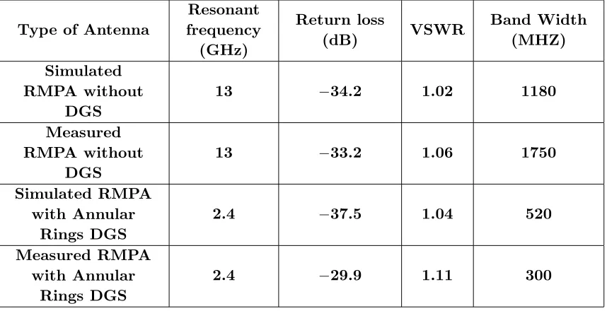
Table 3. Comparison of simulated and measured results of proposed antenna with and without DGS using HFSS.
Type of Antenna
Resonant frequency (GHz) Return loss (dB) VSWR Band Width (MHZ) Simulated RMPA without DGS
13 −34.2 1.02 1180
Measured RMPA without
DGS
13 −33.2 1.06 1750
Simulated RMPA with Annular
Rings DGS
2.4 −37.5 1.04 520
Measured RMPA with Annular
Rings DGS
2.4 −29.9 1.11 300
Table 4. Comparison in gain, directivity and bandwidth of proposed antenna with and without DGS.
Type of Antenna Resonant frequency (GHz) Gain (dB) Directivity (dB) Bandwidth (GHz) Simulated RMPA antenna without DGS
13 5.64 6.54 1.18
Simulated RMPA antenna with Annular Rings
DGS
2.4 1.68 3.85 0.52
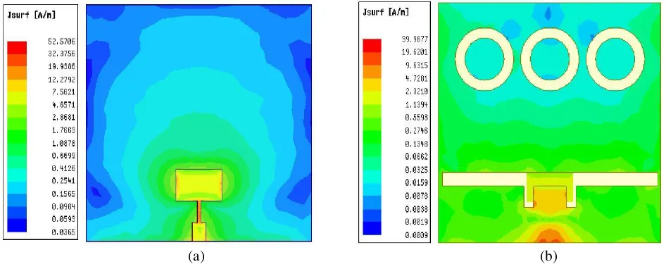
3.3. Current Distribution
(b) (a)
Figure 8. The Surface current distributions at (a) 13 GHz without DGS and (b) 2.4 GHz with DGS in HFSS.
3.4. Radiation Pattern
The radiation patterns shown in Fig. 9 and Fig. 10 are obtained for the patch antenna with and without DGS. The gain obtained is 5.64 dB at 13 GHz, and for our DGS antenna at 2.4 GHz the simulated gain is about 1.68 dB. This reduction in gain is described by the increase of lateral and longitudinal radiations due to the surface wave propagation. Specifically, these radiations adversely influence the main lobe power, and therefore a decrease of the gain is produced.
Figure 9. Measurement and simulation radiation patterns for with and without DGS (E-plane).
Figure 10. Measurement and simulation and radiation patterns for with and without DGS (H -plane).
The proposed design models are structured and verified at different slot lengths. Fig. 11 shows the top and bottom views of the proposed models with and without DGS structures.
(b) (a)
Figure 11. (a) Top and (b) Bottom view of the proposed models.
Figure 12. Simulated Return loss for the pi slot of different lengths ‘a’.
(b)
(a) (c)
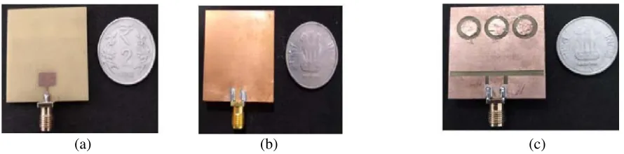
Figure 13. Photograph of fabricated of proposed antennas. (a) Top view, (b) bottom view without DGS (ground view) and (c) bottom view with DGS (ground view).
4. FABRICATION AND MEASUREMENT
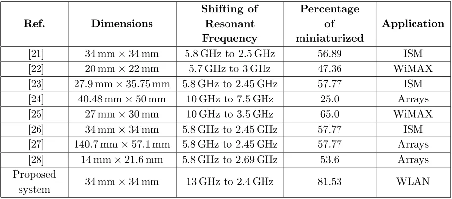
Table 5. Comparison between proposed antenna with other published literature.
Ref. Dimensions
Shifting of Resonant Frequency
Percentage of miniaturized
Application
[21] 34 mm×34 mm 5.8 GHz to 2.5 GHz 56.89 ISM
[22] 20 mm×22 mm 5.7 GHz to 3 GHz 47.36 WiMAX
[23] 27.9 mm×35.75 mm 5.8 GHz to 2.45 GHz 57.77 ISM
[24] 40.48 mm×50 mm 10 GHz to 7.5 GHz 25.0 Arrays
[25] 27 mm×30 mm 10 GHz to 3.5 GHz 65.0 WiMAX
[26] 34 mm×34 mm 5.8 GHz to 2.45 GHz 57.77 ISM
[27] 140.7 mm×57.1 mm 5.8 GHz to 2.45 GHz 57.77 Arrays
[28] 14 mm×21.6 mm 5.8 GHz to 2.69 GHz 53.6 Arrays
Proposed
system 34 mm×34 mm 13 GHz to 2.4 GHz 81.53 WLAN
5. CONCLUSION
In this paper, we have built an innovative approach of miniaturized rectangular microstrip patch antenna by utilizing DGS strategy. Initially, the proposed antenna without DGS is tested at 13 GHz. The objective of this work is to move the resonance frequency from 13 GHz to 2.4 GHz. By inserting our pi-shaped slot with three annular rings as DGS on the ground plane of the patch antenna, the surface current path is wandered, and hence the antenna electrical length is increased. So by increasing the antenna electrical length, the resonance frequency is shifted. After the accomplishment, we have gained a great understanding between simulated and measured results. A miniature rectangular microstrip patch antenna has been created, examined, and approved for WLAN applications.
ACKNOWLEDGMENT
We express gratitude toward Mr. B. T. P. Madhav, Professor in K. L. University, Andhra Pradesh, India, for enabling us to use all the hardware and solvers accessible in his research center.
REFERENCES
1. Bhadouria, A. S. and M. Kumar, “Wide Ku-band microstrip patch antenna using defected patch and ground,”IEEE International Conference on Advances in Engineering &Technology Research (ICAETR-2014), 1–2, Aug. 2014.
2. Chai, W., X. Zhang, and J. Liu, “A novel wideband antenna design using U-slot,” Progress In Electromagnetics Research, Vol. 3, No. 7, 2007.
3. Casu, G., C. Moraru, and A. Kovacs, “Design and implementation of microstrip patch antenna array,”IEEE, 2014.
4. Kaur, N., N. Sharma, and N. Singh, “A study of different feeding mechanisms in microstrip patch,”
International Journal of Microwaves Applications, Vol. 6, No. 1, Jan.–Feb. 2017.
5. Chitra, R. L., B. R. Karthik, and V. Nagarajan, “Double L-slot microstrip patch antenna array for WiMAX and WLAN,” IEEE Advancing Technology for Humanity, 2012.
7. Prasad, P. C. and N. Chattoraj, “Design of compact Ku band microstrip antenna for satellite communication,” International Conference on Communication and Signal Processing, India, Apr. 3–5, 2013.
8. Dubey, S. K., S. K. Pathak, and K. K. Modh, “High gain multiple resonance Ku-band microstrip patch antenna,” Applied Electromagnetic Conference (AEMC), IEEE, 2011.
9. Werner, D. H. and S. Gangul, “An overview of fractal antenna engineering research,” IEEE Anlennas and Propagation Magazine, Vol. 45, No. 1, Feb. 2003.
10. Dong, Y. and T. Itoh, “Metamaterial-based antennas,” Proceedings of the IEEE, Vol. 100, No. 7, Jul. 2012.
11. Wu, Y. Q. and T. Fu, “The study on a patch antenna with PBG structure,” Third International Symposium on Intelligent Information Technology Application, IEEE Computer Society, 2009. 12. Tirado-Mendez, J. A., M. A. Peyrot-Solis, H. Jardon-Aguilar, E. A. Andrade-Gonzalez, and
M. Reyes-Ayala, “Applications of novel defected microstrip structure (DMS) in planar passive circuits,” Proceedings of the 10th WSEAS International Conference on CIRCUITS, 336–369, Vouliagmeni, Athens, Greece, Jul. 10–12, 2006.
13. Wei, K., J. Y. Li, L. Wang, R. Xu, and Z. J. Xing, “A new technique to design circularly polarized microstrip antenna by fractal defected ground structure,” IEEE Transactions on Antennas and Propagation, 2016.
14. Xie, H.-H., Y.-C. Jiao, K. Song, and B. Yang, “Miniature electromagnetic band-gap structure using spiral ground plane,”Progress In Electromagnetics Research Letters, Vol. 17, 163–170, 2010. 15. Arya, A. K., M. V. Kartikeyan, and A. Patnaik, “Efficiency enhancement of microstrip patch
antennas with defected ground structure,” Proceeding of International Conference on Microwave, 729–731, 2008.
16. Zulkifli, F. Y., E. T. Rahardjo, and D. Hartanto, “Mutual coupling reduction using dumbbell defected ground structure for multiband microstrip antenna array,” Progress In Electromagnetics Research Letters, Vol. 13, 29–40, 2010.
17. Nath, S. and S. Rana, “The design and development of microstrip patch antenna using simulation studies by ADS,”International Journal of Electronics Signals and Systems (IJESS), ISSN No. 2231-5969, Vol. 1, No. 2, 2012.
18. Weng, L. H., Y. C. Guo, X. W. Shi, and X. Q. Chen, “An overview on defected ground structure,”
Progress In Electromagnetic Research B, Vol. 7, 173–189, 2008.
19. Guha, D., S. Biswas, and Y. M. M. Antar, “Defected ground structure for microstrip antennas,”
Microstrip and Printed Antennas: New Trends, Techniques and Applications, John Wiley & Sons Ltd., ISBN: 978-0-470-68192-3, 2011.
20. Kumar, A. and K. V. Machavaram, “Microstrip filter with defected ground structure: A close perspective,” International Journal of Microwave and Wireless Technologies, Vol. 5, No. 5, 589– 602, Aug. 2013.
21. Er-Rebyiy, R., J. Zbitou, M. Latrach, A. Tajmouati, A. Errkik, and L. El Abdellaoui, “New miniature planar microstrip antenna using DGS for ISM applications,” TELKOMNIKA, Vol. 15, No. 3, 1149–1154, Sep. 2017.
22. Elftouh, H., N. A. Touhami, and M. Aghoutane, “Miniaturized microstrip patch antenna with defected ground structure,”Progress In Electromagnetics Research C, Vol. 55, 25–33, 2014. 23. Ghaloua, A., J. Zbitou, L. El Abdellaoui, and M. Latrach, “A miniature circular patch antenna
using defected ground structure for ISM band applications,” ICCWCS’17, Larache, Morocco, Nov. 14–16, 2017.
24. Oulhaj, O., N. A. Touhami, M. Aghoutane, and A. Tazon, “A miniature microstrip patch antenna array with defected ground structure,”International Journal of Microwave and Optical Technology, Vol. 11, No. 1, Jan. 2016.
26. Er-Rebyiy, R., J. Zbitou, M. Latrach, A. Tajmouati, A. Errkik, and L. El Abdellaoui, “A novel design of a miniature low cost planar antenna for ISM band applications,” ICCWCS’17, Larache, Morocco, Nov. 14–16, 2017.
27. Ghaloua, A., J. Zbitou, M. Latrach, and A. Tajmouati, “A novel configuration of a miniature printed antenna array based on defected ground structure,” International Journal of Intelligent Engineering and Systems, Vol. 12, No. 1, 2019.
28. Elftouh, H., N. A. Touhami, and M. Aghoutane, “Miniaturized microstrip patch antenna with spiral defected microstrip structure,”Progress In Electromagnetics Research Letters, Vol. 53, 37–44, 2015. 29. Huang, Y. and K. Boyle, Antennas from Theory to Practice, A John Wiley and Sons, Ltd.,
Publication, 2008.
![Figure 1. Some basic configurations of DGS [19, 20].](https://thumb-us.123doks.com/thumbv2/123dok_us/1911029.1250518/2.612.164.455.80.310/figure-basic-congurations-dgs.webp)