•
>-...:
"'II
.g
~
c
_.
en
::a;-n
g
-a
-c»
...
-J
]
]
]
1
]
]
]
•
]
]
~
GENERAL
COR ROBOTPOR
ICS
ATION
--t
•
...,
-o
"
~
C
_ Ien
;I;
Cl
o
i
a
--CD
..
-DATE
MAY 82 AUG 83 OCT 83 MAR 84 NOV 84 JAN 85
General Robotics Corporation
RXV21 USER MANUAL
740-J02R-EO
Revision Table
DESCRIPTION
!;fanual Edit
Manual Corrections
Manual Reformat:Table 2.4-D, re:Qume Drive, Added Revised and Corrected.
Additions and Corrections
NOTE: Date indicates current level of manual revision.
General Robotics Corporation 57 North Main Street
Hartford. WI 53027
RXV21 User's Manual
TABLE OF CONTENTS
1.
2.
General Information •
•
•1.1
1.2
Introduction •
Components • • • • •
1.3 Compatibility •
1.3.1 1.3.2 1.3.3 1.3.4 1.3.5 1.3.6
Logical Track Sector Header Data Field
Format Field
Recording Scheme ~
Double Frequency (FM) DEC Modified MFM
• •
• •
1.3.7 Cyclic Redundancy Check •
1.4 Specification •
Installation •
• • • • • • •
2.1 Configuration • • •
2.1.1 Address Vector Selection 2.1.2 Device Interrupt Priority. 2.1.3 Bootstrap.
2.1.4 Write Precompensation • 2.1.5 Write Current Control 2.1.6 Drive and Side Selection 2.2 Drive Configuration
2.3 Cabling
2.4 Controller Installation
2.5 Initial Operation and Checkout
3. Functional Description • • •
3.1 General • • •
3.2 Register Definitions • •
RXVDB Data Buffer • 3.2.2
3.2.3 Extended Status Registers 3.3 Command Protocol
Fill Buffer • Empty Buffer Write Sector Read Sector •
Set Media Density • Read Status
• • • • • • 3.3.1 3.3.2 3.3.3 3.3.4 3.3.5 3.3.6 3.3.7 3.3.8
Write Deleted Data Sector • Read Error Code • • • •
• • • • • •
• •
• • • • • • • • ••
• • • • • • • • • • •. .
.•
• •• •• •
• • • •
• • • ••
•
• •
• • • • • • • • • • • • • ••
•
• • • • • • • • • •• •
• • • • • • • • • • • •• •
• • • ••
• •
• ••
•
• • • • • • • • • • • • • • • • • • 4. Controller Operations• • •
•
•
••
•• • • • • • •
• ••
4.1 General • • • • • • • • • • • •
• •
• • •4.2 Bootstrapping the Controller • • • • • • • • •
• •
4.1.1 Bootstrap Operation. • • • •
• •
••
4.3 Format Operations •
• •
• • • • • • •4.4 Fill/Write Operations • • •
• •
• •
•4.5 Read/Empty Operations • • • •• • • •
•
••
4.6 Write Current Control • •
•
•
• • • • •• •
4.7 Write Precompensation • • 4.8 Power Fail Protection
4.9 Operation and Format Using RTll
.
.
.
.
.
.
.
.
. .
.
.
. .
.
Copying a DY Compatible Release DisketteRXV21 User's Manual
·
.
. . .
.
.
.
.
.
.
· . .
· .
.
.
.
4.9.14.9.2 Installing DY under RSX. • • • • • •
. .
.
. . .
43 43 44 44 45Rxv21 IIser's Manual
1. GENERAL INFORMATIon
The purpose of this manual is to provide the user adeouate information to
configure and operate the RXV21 floppy disk cont~oller. The information
provided should clarify the controller connection to any Shugart compati
-ble drive and assist in the selection of associated interface options.
Both register definition and command protocol are provided for reference
and as an aiel. in development of user software. Operational procedures
outline the use of the controller features as well as explaining
opera-tion in an RTll* software environment.
1. 1 Introduction
The RXV21 is a dual densitr controller compatible w1th the DF.r:* RX02*
floppy disk system. Configured with any Shu~art compatihle drive,- it is
a direct replacement for the DEC RXV21 subsystem. The controller. provid
-es either single density encoding comeatible with I~M 174n equipment ~
double density enc.:oding, providing 512K bytes of storage 011 a sln.21e
diskette. Uhen configured with two drives, each drive may operate at a
different density.
All electroLlics are COLltained on one dual height mociule which p]u!":s
ril-rectly into any standard LS!-ll* hackplane and interfaces throu~h a~
conductor ribbon cable to any Shugart compatible drive. All controllers
are 100% tested and ready for operation. The controller iR confl,2ureci
for the standard device address 777170 (octal) and interrupt vector 2~4
(octal). The interrupt level is factory set to level four. Features
in-clude:
Transparent firmware bootstrap automatically loads
double density diskettes.
either s1nStIe
.Lormatting capability permits writin~ sector
written headers, and writing the data fields in
ity.
hearlers,
the user
checkiny. the
selected dens
-Jumpers allow user selection of both the ,alternate arlnIess and vector •
.Jymper selectable four-level device interrupt priority comeatihle w1th
the LSI- 1I/23.
Provides power fail protec~ion for data inteStrity.
Write current control signal for tracks greater than forty-three.
Write precompensation for reduced error rates.
Bus Loads: AC-3; DC-I
*TM of Digital Equipment Corporation
"
,RXV21 IIser's Manual
1.2 Components
The controller Is provided with the following: components:
1.3 Compatibility
RXV21 Floppy Disk Controller Module
RXV21 User's Manual
This section discusses the aspects of hardware. software ann -IDedia co
m=--patlbl11ty with ntgital Equipment's RX02 system. The information wl11
aid the user 1n data interchange with foreign systems.
1
Hardware Compatibilityj
The controller 1s compatible '011th the LST-II , LST- ll/2 ann U;T- 11/2"!o
family of processors. All circuity 1s contained on Olle dual hel~ht
module that plugs rllrectly Into any standard LST- II hackplane. Alternate
address selection and a four level device interrupt priority scheme
pro-vide the user added flexibility for expanded system configurat1ons. Shugart compatible drive logic is interf.aced throu~h a SO pin ribhon
con-nector. The interface is compatible with both the ~hu~art model ROO an~
8S0 series drives.
[ ioftware Compatibility \
The RXV21 is completely compatible with RXV21 register definitions and
command protocol. All DEC-supplied software designed to operate with the
,
h
'
I
RX02 system will operate with the controller without mOdifica.t~'~o[n~.~:iR~O~W2r-~
ever, for RX03 usage the
OEe
supplied handler for RTll(DY)
~ a. anII
which does not allow automatic sensing of double side ready. ~e handler
I'
supplied by GRC has been corrected for this funct ion.C;
g
C
!;P-t!::
0 3
. \:Media Compatibility )
The media used with the RXV21 is compatible with the IHH 3740 family of equipment. Either preformatted or blank soft sectored diskettes may he
used with the controller.
1.3.1 Logical Track Format
The diskette surface is divided into 77 concentric tracks numhered 0
76. Each track consists of 26 sectors numbered 1 - 26. The track he~in~
and ends at the index address mark. The track is formatted in such 8 way that this soft index is preceded by the le8din~ edge of the physical
index hole in the diskette. Followin~ the physical 1ndex are 40 hytes of
'FF; data, 6 bytes of '0' data, and the index address mark indicating the
beginning of the track. Following the index adrlress mark is the post
index gap consisting of 26 bytes of 'FF' data and " hytes of '0' data.
The next field is the sector header for sector 1. Following the sector
header is the ID gap conSisting of II bytes of 'FF' data and" bytes of
2
"'fol~ol Indu
RXV21 tlser's Manual
'0' data. The next field Is the data record for sector 1. Followln$t the
data field is the data gap consisting of 2A bytes of 'FF' data and ~
bytes of '0' data. This field leads to the next sector header. Follow
-ing the 26th data record is the pre-index gap consisting of approximately 274 bytes of 'FF' data.
Each track is formatted in the above manner. Refer to Figure 1.1. sector header field of each sector contains information describing the sector and track number. All the ahove fields are recnrded in except as noted in the following sections.
The both
FM
CI.,I. CAll 10 ,~
,
ID r:U h . 1...:1.. Pa . . ~"""t beardno S7UO FH ) l " ' " "" 17 " ' " nI
~ t:
:
.
Figure 1.1
Logica~ Track Format
3
,~
,
~XV21 User's Manual
1.3.2 Sector Reader Field
The header field consists of 7 bytes of information. Precp.rlin~ the header is a field of 6 bytes of '0' data for synchronization. The header and this preamble are always recorded in FM.
1. Byte I. 10 Address Mark - A unique mark consistin~ of I byte o~
FE (hex) data with three missing clock transitions using a r.7
(hex) clock pattern. This mark is decoded by the controller
and indicates the start of the sector header .
2. Byte 2. Track Address - This byte indicates the absolute (0 114 octal) track address. Each sector contains this track information to locate its position on one of the 77 tracks.
3. Byte 3. Zero
4. Byte 4. Sector Address - This byte indicates the absolute (1-32
octal) sector address. Each sector contains this information
to identify its position on the track.
5. Byte 5. Zero
6. Bytes 6 and 7. CRC - This is the 16 bit cyclic redundancy char
-acter and is calculated for each header from the first 5 bytes
of information, using the IBM 3740 polynomial. Refer to r.yclic
Redundancy Check, Section 1.3.7.
1.3.3 Data Field
The data field consists of either 131 (decimal) or 259 (decimal)
information depending upon the recording methocl. PrecedtnlZ
field is a field of 6 bytes 'of '0' data for synchronization.
Tne preamble and data address mark are always written in FH.
data and CRC character are either written 1n FM or modified MFM
upon the formatted diskette density.
bytes of
the data
The user dependinlZ
1. Byte I, Data Address Mark - A uniQue mark consistin~ of a clata
byte (see Table 1.1) vith three mlssin~ clock transitions usinlZ
a C7 (hex) clock pattern. This byte is always written in PM
and is decoded by the controller to indicate the start of the
data field, its recording method (FM vs. MFM). and if the fielrl is a deleted data field.
ADDRESS
I
MARKI
INDEX
I
In
I
DATA
I
DELETED
DATA
INJHC:ATED
DENSITY DATA
N/A
I
N/A
FM
MFM
ModifiedFM
MFM
ModifiedTable 1.1 Address Marks
FC
FE
FR
FD
FR
FQ
~XV21 User's Manual
I
CLOCl{
I
I
I
C
7
I
I
C7
I
I
C7
I
I
r,7
I
C7
I
C7
I
2. Bytes 2 through 12q (FM) or bytes 2 through 257 (MFM modified' User data. This field is recorded in either FM or MFM modi
-fied. Depending upon the encodinp; scheme, either 12R or 2Sli bytes of information can be stored.
3. Bytes 130 through 131 or bytes 25A throup;h 2SQ, CRe - This is the 16 bit cyclic redundancy character and is calculated for
each data field from the first 129 or 257 bytes of information using the IBM 3740 polynomial. Refer' to Cyd ic Redundancy Check, Section 1.3.7. These bytes are recorded with the same encoding scheme as the data field.
1.3.4 Recording Scheme
Two recor'ding schemes are used by the ~~v21: Double freouency (PM) and DEC modified Miller code (MFM). FM is used for single density recordin~
and is compatible ~ith IBM 3740 or DEC: ~~Ol media. nr.c modified MFM is used for recording double density and is only compatible ~ith the DEC R.,·W2 system.
1.3.5 Double Frequency (FM)
FM recording is charactierized by a flux transition at the be~lnning of each bit cell ~hlch is commonly termed a clock pulse or transition as shoYn in Figure 1.2. A logic '1' is represented hy a flux transition
~ithin the bit cell; a logic '0' is represented by the lack of any flux transition ~ithin a bit cell. In FM the bit cell time is 4 microseconds.
5
"
",
••
RXV21 User ' s Manua 1
-
-
>
o
bit
cell
4 uS
o
(
-o
1Figure 1.2
FM Recording Charactistics
1.3.6 DEC Modified HFM
o
MFH recording consists of flux transitions for a lo~lc 'J' and no flux
transitions for a logic '0'. A clock transistlon only occurs between two
consecu t1 ve logic • 0' sta tes as shown in Fl~u re 1.1 he low. The MFM hi t
cell time Is 2 microseconds.
0 0
o
1I
-
I
I
-
I I
-
I I
-
I
- -
D-
-
D C D- - -
I
-
n
I
--
I
-
DI
-bit
--
>
cell (--.
2 uS
Figure 1.3
MFM Recording Characteristics
Table 1.2 summarizes the standard MFM encoding algorithm.
I
---
~~:~
-
----
-
I
-
----
~~:~~:~
-
~~~
~---DN- I DN
I
ON- l eN ONo
1
o
1o
o
1
1
o
1
o
1
1
o
o
o
Table 1.2
Standard MPH Encoding
6
o
o
1
RXV21 User's Manual
Because single density headers are used for both FM and MFM recording formats, and since certain MFM patterns map into single density address marks, a modified algori thm is usen. The mapping occurs ~hen a nata pat
-tern of exactly four consecutive '1' states is encoded. Whenever this pattern is encoded a special algorithm is applied. Table 1.3 defines the encoding algorithm for this special case.
DATA
On 5
I
Dn 4I
Dn 3I
nn 2I
nn 1I
nn0 1 1 1 1
I
0X 0 1 0
o
0I
1 0o
0I
I 0Cn- S Dn-S Cn-4 Dn-4 Cn-3 Dn-3
_
1
Cn-2 On-2 Cn- l0n- l i Cn nnENCODED DATA
Table 1.3
Modifying Algorithm (5pecial Case)
When reading double density data fields the controller checks for a miss -ing clock bit bet~een t'Wo zero data cells, and if found, substitutes ones
for the two zero data bits (generated by the special encodin~ algorithm).
1.3.7 Cyclic Redundancy Check
Each sector header field and data field has a two byte CRC character ap
-pended. This 16 bit character is the remainder that results ~hen
dividing the data bits [represented as a polynomial H(x)] by a ~enerator polynomial G(x). The polynomial use for IBM 3740 is G(x)-xlfi+x12+x,+I. For the sector header the data bits include byte 1 through hyte'. For
an FM data field the data bits include byte I through byte t2q. For an MFM data field the data bits include byte 1 through byte 2S7.
1.4 Specification
RECORDING TECHNIQUE:
Single Density Double Density
POWER REQUIREMENTS:
Voltage Current
ENVIRONMENTAL:
Temperature Humidity
IBM 3740 FM
DEC Modified MFM
5 VDC (from LSI- It backplane)
2.5 A typical
o
-
45 degrees C10 - 95 % non-condensing
7
'.
RXV?l User's Manual
2
.
INSTALLATION
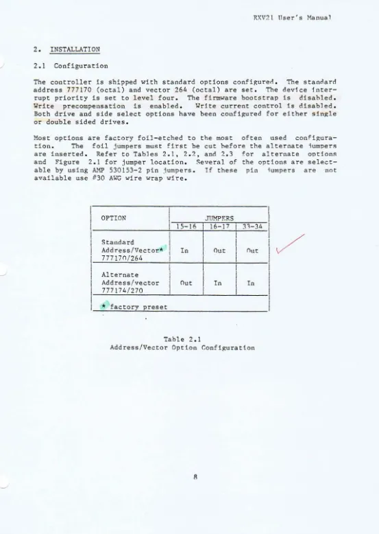
2.1 ConfigurationThe controller 1s shipped ulth standard options conflgurerl. The stanrlaro
address 777170 (octal) and vector 264 (octal) are set. The Clev1.ce inter
-rupt priority Is set to level four. The firmware bootstrap Is disabled.
Write precompensation is enabled. Write current control Is disabled.
Both drive and side select options have been confl~ured for eithe. sln~le or double sided drives.
Most options are factory foil-etched to the most often used confl~ura
tlon. The foIL jumpers must first be cut he fore the alternate 1umper~
are inserted. Refer to Tables 2.1. 2.2, and 2.3 for alternate OPtion~
and Figure 2.1 for jumper location. ~everal of the options are select
-able by using A.~ 530153-2 pin jumpers. I f the~e pin ;umpe-rs a-re oot
available use P30 AWe wire wrap wi-re.
OPTION ..TIIMPF.RS
15- 16 16- 17 31-34
Standard
I
i
Add ress/Vector*
I
In
OutI
Out777170/264
I
Alternate
Address/vector Out
I
n
In
777174/270
*
factorz :eresetTable 2.1
Address/Vector Option Confi~uratton
R
I
I
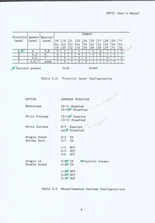
RXV21 IIser's Manual
Assert \Monitor
Jumper Priority
Level Level Level IA 19 21 \22 \24 25 127 12A 30
"
to to to to to to
I
toI
to to to19 20 22 23 25 2n 2R 2q 11 32
4 • 4 5,6 0 I 0 I T
n
0T
In
5 4,5 6 0 I
I
In
In
0 In
I
T
6 4,0 7 I I
n
n
In
T
Tn
T
I
07 4. 1),7 none I I
o
I
I 0 0 I In
n
i
T
* factory preset I"'INTable 2.2: Priority Level Configuration
OPTION
Bootstrap
'.Jrite Precomp
Write Current
Single Sided Drives Only
Single or
Double Sided
JUMPERS FUNCTION
10- 1l Enabled 10-43* Disahled v
13- 1 t..* Ena bled 13- 12 Disahled
8-q out*
Enahled /
Disabled
2-3 IN 5-7 IN
1-2 OUT 4-5 OUT 5-6 OUT
2-3*
IN
*-factory oreset 4-5'11;.IN
1-2* OUT 5-"* OUT 5-7* OUT
Table 2.3 Miscellaneous Options Confi~urattons
9
·'1' •
.,
,
. J:. '.
.
-11
19-'
J
V
RXV21
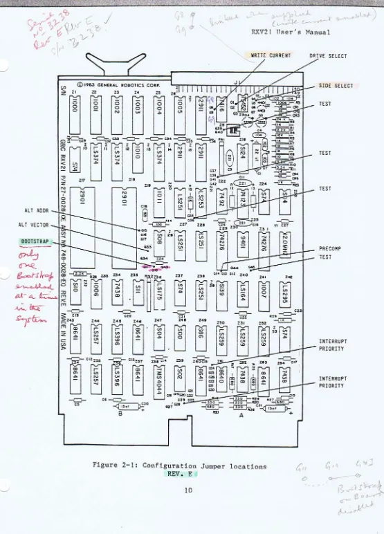
Figure 2-1: Configuration Jumper locations
REV. E
10
~\'}1\""""J... ~t
'>- .. t,1 GI( ... ,,,...U- c.-~
ITser's Manual
DRIVE SELECT
SlOE SELECT
TEST
PREeo"p
_ ·TEST
INTERRUPT
- PRIORITY
RXV21 User's Manual
2.1.1 Address Vector Selection
The controller is shipped with the
DEC
standard device address and vector assignments preset to 777170 (octal) and 264 (octal), respectively. Any change in the~e assignments would necessitate a chan~e in SY5tem soft-ware. However, and alternate address and vector assi~nment is selectable and is defined as 777174 (octal) and 270 (octal) respectively.These assignments are typically used when more than two drives are needed; two controllers would be required and the second controller would be configured for the alternate address and vector. To select the alternate address and vector, first cut the foil between Gl'5 and Glfl.
Jumper GIl) to
Gl7
and jumper G33 to r.34 as shown in Table 2.1.2.1.2 Device Interrupt Priority
The RXV21 supports the four level device interrupt priority scheme com
-patible with the LSI-11/23. The controller asserts interrupt requests and monicors higher level request lines durtn~ interrupt arbitration as
described in Table 2.2. The level four request is always asserted hy the cOlltroller, regardless of its priority, to maintain compatihltlty with the LSt-ll and LSI-tI/2 processors.
The interrupt priority level is configured to level four at the factory.
I f a different interrupt level is desired the following foil-etched iump
-ers must be cut. Refer to Table 2.2 for the proper .iumper!'> to insert for the desired priority level.
G19
-
G20
G22 - G23 G24 - G25 G28 - G29
G30
-
G31
2.1.3 Bootstrap
The controller board incorporates a transparent firmware bootstrao. The bootstrap is initiated whenever program execution is started at location 773000 (octal), homing both drives to track O. Next, track I, sector I of unit 0 is read and the diskette density is determined. I f the disk-ette is Single density, sectors I, 3, 5, and 7 are loaded into memory starting at location
O
.
If the diskette is double density, sectors 1 and 3 are loaded. Program execution is then transferred to location O. Con -trollers are shipped with this feature disabled. To enable the bootstrap remove the jumper from G43-GlO and insert the .1umper hetween G1n and (:11 as shown in Table 2.3.1 I
, t
RXV?'l IIser's Manual
****CAUTIONARY NOTE****
Rev D boards had a layout error which
swapped GIn and GIl. G~3 a60ul n ver co.nne,cte. 0 GI on these or any other
boards.
.,---~-~--~---,
NOTE -
--r. nl-Y. boot r;9. should be enabled In a
system for proper operation. I f faAo"th,~
bootstrap exists in the system. it mu~
be d1.sa Ie before enahl1ng the control-ler bootstrap.
2.1.4 Write Precompensatlon
v,.,
\;;> 0;1
r-The RXV21 controller provides harnware write precnmpensatlon to reduce
the bit shift exhibited by all drives as the recorded flux density in
-creases. The controller recognizes the patterns which produce hit shift
and prec.ompensates the written pattern. This unique feature allows the
controller to perform reliably with anv Shugart Compatible drive.
Controllers are shipped with this feature enablerl anrl it is recommended
that for more reliable operation the feature not be disabled. 'Rowevet',
if so desired, the featut'e can be defeated bY--cuttin~ the foil-etcherl
jumper between G13 and G14 and inseninR a ,iumpet' between (';12 and GIl as
shown In Table 2.3.
2.1 .5 Wt'ite Curt'ent Control
The RXV21 provides the necessary signal to reduce the write current for
tracks greater than forty-tht'ee. This signal 1s available at pin 2 of
the 50 pill. t'ibbon connector.
Since the Shugart model BOO series single sided drives do not re~uit'e a
write current Signal, the contt'oller is shipped with this feature dis
-abled. However, the double sidQd 850 series drives do suppot't wrtte
current control. and enabling this feature is recommended for reliable
operation. This may be accomplished by jumpering pins r;R and r.9 as shown
in Table 2.3.
2.1.6 Drive and Side Selection
The controller featut'es several options for both drlve and
tion. The side select output can be disabled, allowin~
single sided drives only. The controllet' can he configured
Single or double sided drives. Proper jumperlng allows one
12
side selec -operation on
for either
douhle sided
r~'w (
~.
"
,
,
,
•
I
I
I
I
I
RXV21 Tlser's Manual
drive to be addressed as two drives where side 0 appears as .drive and side 1 appears as drive 2. However
seeK-e-r"t"ors f a seek to a diffE""nt
a~cesses on drive B, becau~e the controller is expecting the two drives
to have separate seek mechanisms and finds that it is not on the correct track.
The controller, when shipped, is configured for either single or nouhle
sided drives. If double sided drives are used, it is recommended that
l
the write current control be enabled as described in Section 2.1.5.Before selecting alternate options the foil-etched jumper between r,A and
GS must be cut. For alternate configurations refer to Table 2.3.
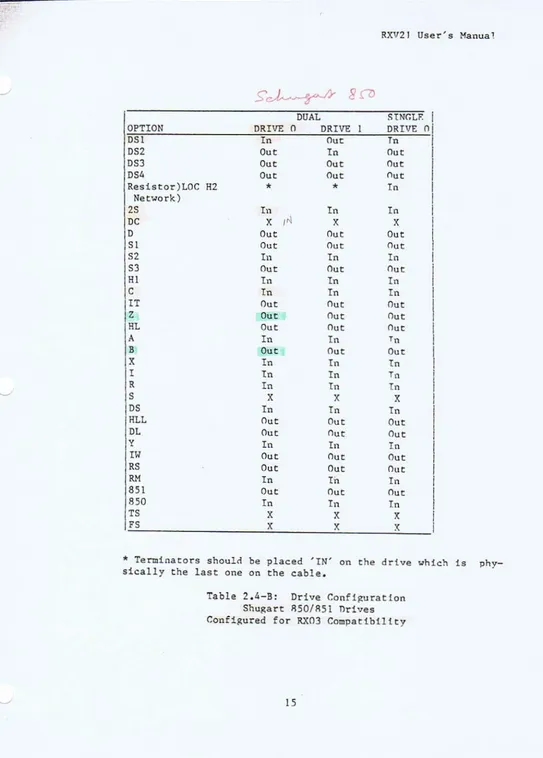
2.2 Drive Configuration
For proper operation, the floppy drives must he configured with attp.nt10n to several options. The controller uses radial drive selection. Thus the drive(s) should be correspondingly configured. Yhen two drives are used, the first should be drive 1 and the second drive 2. A particular drive 1s selected and remains selected after a functton 1s complete to allow the controller to poll drive status. A separate head load signal 1s provided by the controller for read and write functions on the disk -ette. The 'IN USE' logic of the drive should be configured as a Function of head loading. Since the drives are homed without loading the heads during an initialize command, the drive should he configured to provide stepper motor power independent of head loadin&... Refer to Table 2.4 for
details concerning these and other options.
.~"
RXV21 "ser's Manual
)~G-%
8<.>0
OUAL ~TNr.LF:
I
OPT DESCRIPTION
(IC);
nRtVE 0 nRTVF. flRT\TF. 0I
051 Drive Select 1
O,r
In
OutIn
I
052 Drive Select 2 Out
In
OutI
053 Drive Select 3 J Out Out Out
I
054 Drive Select 4 Out Out Out
I
A Radial head loading option
/
'n
Tn
In
B Radial head loading option ,1tn III
In
I
C Head load option
In
Tn
In
I
0 In use option Out Out Out
X Radial head loading option
IN
Out Out OutI
WI' Inhibit write when protect
In
In
Tn
I
NP Allow write when protect Out Out Out
I
os
Stepper power from drive selectI
n
In
In
I
HL Stepper power from head load Out Out Out
I
Z In use from drive select I Out nut Out
y In use from head load 0 r
In
In
In
I
R Ready output
In
In
Tn
I
I
Index outputIn
Tn
Tn
I
DC Disk change output X X X
I
5 Sector output X X X
I
800 Sector option Disable
In
Tn
Tn
801 Sector option Enable Out Out Out
I
L -5V DC Bias
In
In
In
I
Tl Terraination HL
,
,
In
I
T2 Terrai nation Drive Select
*
*
Tn
I
T3 Terraination Direction
*
*
In
I
T4 Terrainat ion Step
*
*
Tn
I
TS Termination Write Oata
*
*
In
I
T6 Tennination Write Gate
*
*
I
n
I
*
Temillators should be placerl 'IN' on the drive which is physically the last one on the cable.Note: 800 SerIes drives may requIre 10 millisecnnd step
erate properly. ThIs PROM Is located in socket Z7.
PROM is 3 millisecond.
Table 2.4-A: Drive Configuration
Shugart 800/ROI Drives
14
rate ~RnM~ to op
RXV21 User's Manua'.
S'~~
8'?J
DUAL ~tNr.LF.
1
OPTION DRIVE
0
DRIVEDRIVE
01
D
S
I
In
OutTn
I
DS2
OutIn
OutDS3
Out Out OutI
DS4
Out Out OutRes1stor)LOC
H2
*
*
In
1
Network)
1
2S
In
In
In
1
DC
XI"
X X1
D
Out Out OutI
SI
Out Out OutS2
In
In
In
1
S3
Out Out Out1
HI
In
In
In
1
C
In
In
In
1
IT
Out Out OutI
z
Out Out OutHL
Out Out Out1
A
In
In
Tn
1
B Out Out Out
I
X
In
In
In
I
In
In
Tn
I
R
In
In
In
S
X X X1
DS
In
In
In
HLL
Out Out OutDL
Out Out Outy
In
In
In
IW
Out Out OutRS
Out Out OutRM
In
In
In
851 Out Out Out
850
In
In
In
TS
X X XFS
X X X*
Terminators should be placed 'IN' on the drive which is phy-sically the last one
on
the cable.Table 2.4-8: Drive r.onf1~ration
Shugart R50/R51 Orives Configured for RX03 Compatibility
RXV21 Ilser's Manual
OPTION DRIVE
DUAL
o
DRIVE<INGLF
I
nRTVf. nI
OSI OS2 OS3 OS4 RNI S R I C D DC 2S 51 S2 S3 DL DO X A B RI RR NP lJP IU Y Z HO DR E SS HS N5 OS
FS
TS On Off Off Off Out X In In In Out Out In Out In Out In In Out In In In In Out In Out In Out In Out X In Out In Out Out In. Off Tn Off Off In X In In In Out Out In Out In Out Tn In Out In In In In Out In Out In Out In Out X In Out In Out Out In OnOff
I
Off
II
Mf In X In In In Out Out Tn Out Tn Out In In Out In In Tn In Out Tn Out In Out In Out X In Out Tn Out Out Tn
*
Terminators should be placed 'TN' on the drive which i~physically the last one on the cable.
Table 2.4-C: Drive Confi~urat10n
CDC PIN 9406- 2/3 Drives
Configured for RX03 Compatibility
--
....
---~
r
,
~
RXV21 Tlser's Manual
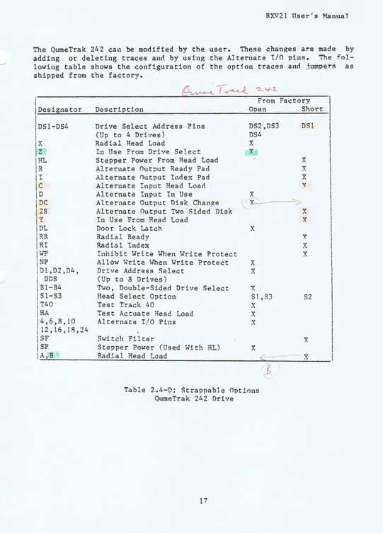
The QumeTrak 242 can be lIIodified by the uset'o TheRe changes are made by
adding 0'[" deleting traces and by using the A] ternate 1/0 pins. The
fol-lowing table shows the configuration of the option tt'aces anc! jumpers as
shipped from the factory.
Designator
DS I-DSl!
x
Z HL Rr
Co
DC 2S y Dt RRRr
""
NP
01,02.04,
DDS
BI-34
S 1-53
T40
HA
4,6,8.10
12.16,lR,24
SF
SP
A,BDescription
Drive Select Address Pins
(Up to 4 Drives) Radial Head Load
In Use From Drive Select
Stepper Power From Head Load
Alternate Output Ready Pad Alternate t")utput Index Pad
Alternate Input Head Loan Alternate Input In Use
Alternate Output Disk Chan~e
Alternate Output Two ~ided Disk
In Use From Head Load
Door Lock Latch
Radial Ready
Radial Index
Inhibit Write When Write Protect Allow Write When Write Protect
Drive Address Select (Up to 8 Drives)
Tvo, Double-Sided Drive Select
Head Select Option
Test Track 40
Test Actuate Head Load Alternate I/O Pins
Switch Filter
Stepper Power (Used With AL) Radial Read Load
From Open DS2,DS3 OS4 X X X
X
-X X X X 51,S3 X X X X
1,
Table 2.4-0: Strappable Optlnns QumeTrak 242 Drive
RXV21 User's Manual
2.3 Cabling
A 50 conductor ribbon cable connect" the controller to any ~hu2art
com-patible drive(s). If the optional cahle is purchase~ with the
controller, connect the socket connector to the "in pin heaeler locateel at
the edge of the controller board. Observe the alignment of pin 1 of the
socket connector and header as indicated by the arroys shown in Fi,2ure
2.2. The tyo 50 pin connecto~s should he comlected to the corespondin~
drives, again observing the location of pin 1. If the optional cahle is
purchased from an independent source, the followinr. list of materials (or
equivalent) will help in the construction of the requ1 reel cahle.
QTY DESCRIPTION MFG pIN
50 pin socket connector 3M ;\"'25-100n
2 50 pin edge connector 3M 3"'IS-0ClOl
AIR 50 conductor ribhon cable 3M 1365/50
PIN 1
--=
=
~
=9"
R
Ir'
~~----{j-(,t.,-c..BLE
(50-pin Ribbon CableJ- __ ~ ____ __
DRIVE
(SHUGART
COMPATIBLE)
PIN 1
~.lo-_-5CX:KET CONNECTOR
Figure 2.2
Drive/Controller Cabling
18
•
l
I
RXVZI User's Manua'
The connector pins illustrated in Figure 2.3 are compatible with hoth the Shugart 800 series and 850 series drives. Any drive that has hoth a Shu-gart compatible interface and connector should function properly with the controller.
I 2 ----) /TG 43
3 4
5 6 7 8
I
9
I
10
1
(- - - - -11 12 I+-~13~---"14;-t.
1
-
---
-
> IS 16 I~tl~7=t~1~8~----
~ 19 20 (----
)
21 22
<
---
--t2~3!=t
::
2~4~
1
t--;2",5-+-;;2,;-6 -+1--->
27 28
I
---->29 30 I
3 I 32
33 34 I --- - -)
35 36 I
----
>
+-3~7~~3~8~t--->39 40 .---)
+-4;;
1
'-+":4;';2~
1
·
<---~
454~3 ~44~
46 11<
<------
-
---47 48 I
49 50 I·
/TWO SIDED
/
5IDF.
SELECT/READ LOAD
/U.'nEX /READY
/D
RI
VE
SELECT1
/DRIVE SF-LECT 2
/DIRECTIO
N
/STEP
/HRITF. DATA
/WRITE GATE /TRACK I)
nffi.!TE
PROTECT
/READDATA
NOTE:
AllOnD
pin numbersindicates a negated or
signal flow.
are connected to ground.
low true signal. Arrows
'Figure 2.3
Connector Pin Definitions
2.4 Controller Installation
This symbol. (/).
indicate direction of
The controller can be inserted and will function in any
LSI-II
bus slot provided that hath interrupt and DMA continuity is maintained. Since these signals are daisy chained through the bus slots, no unusen slotsbetween the LSI- II processor and the floppy controller may exist. Deter-mine the order that the priority chain follows by consulting the documentation supplied with the LSI- II system. Note that when two
inter-19
.
RXV21 User's Manual
rupts of the same priority level are asserted, the closer a device is located to the processor, the higher its priority level.
2.5 Initial Operation and Checkout
Before the following procedures are done, verify that the controller has been configured as described in Sections 2.1 through 2.4.
--- NOTE
The bootstrap must be disabled for the following procedures.
1. Apply AC and DC power to the drivers). The spindle(s) should begin to rotate. The in-use indicators on both drives should be off.
2. Place the RUN ENABLE/HALT Rwitch on the processor to the HALT position and turn on the processor. An '@' character shoul~ be printed on the terminal signifying that console onT has heen entered. Both drives (first drive 1, then drive 0) will step the heads inward 10 tracks, then step the heads outward until the home signal is detected. The heads will not load, and, if the drive is configured as per Section 2.2, the in-use indica-tors will not light. If the above events do not occur, check the cabling and drive power supplies.
3. Place a preformatted scratch diskette in drive O.
4. If the standard address assignment is selected, open the com-mand and status (CS) register using ODT by typing 177170/ on
the terminal. The processor will display the contents of the CS register. If the controller is operating properly a 004040 (octal) should be printed. Deposit a 40000 (octal) in the CR register by typing 40000<CR>. This command will initialize the controller. Both drives should calibrate for home position. First, drive 1 steps inward 10 tracks then outward one track at a time until the drive indicates track 0 has been reached. The procedure is repeated on drive O. After both drives are cal-ibrated, the head on drive
n
is loaded. Sector 1 of track 1 on drive 0 is read into the controller buffer. This operation is indicated by the in-use LED on the drive. Only the LED on drive 0 will be turned on, indicating the head load operation. The LED will remain on for a short time after the read opera-tion is complete.If, after initializing, the drives do not calihrate or the LEn is not activated, check the cabling and power supplies.
RXV21 User's Manual
5. Reopen the CS register (location 177170 octal) using
aDT
as de-scribed above. The contents of this location should be 004040 (octal) or 104040 for an unformatted diskette. F.xamining the next location 177172 (octal) should yield either a 20fi (octal) for an unformatted diskette, or 246 (octal) for a formatted diskette. For a detailed description of the register protocol and bit definition, refer to Section 3.6. If the above procedures function as rlescribed, the controller is ready for use. Either diagnostics or an operating system can be booted. For details on bootstrapping refer to Section
4.
7. If the above procedures cannot be validated, consult the fac-tory or your local representative for assistance.
RXV21 User's Manual
3. FUNCTIONAL DESCRIPTION
3.1 General
This section describes device registers and command protocol for the RXV21.
All software control of the RXV21 is performed by means of two device registers: the command and status (RXVCS) register and a multipurpose data buffer (RXVDB) register. These registers are normally assigne~ the bus address 777170 (octal) and 777172 (octal), respectively. ~e
regis-ters can be read or loaded, with a few exceptions, using any instruction referring to their addresses.
The ~~VCS register passes control information from the CPH to the
con-troller and reports status and error information from the controller to the CPU. The ~~VDB is provided for additional control and staus infor-mation between the CPU and the controller. The information that is
present in the RXVDB at any given time is a function of the controller operation in progress.
The controller contains a sector buffer capable of storing a complete sector. For read/write operations the buffer is either filled before a write command or emptied after a read command under DMA control. nUTing a write command the controller locates the desired sector and the huffer information is transferred to the diskette. During a read operation the desired sector is located and the sector data is transferred to the buffer.
3.2 Register Definitions
3.2.1 RXVCS Command and Status Register
The format of the RXVCS regtster (777170 octal) is shown helow. Func-tions are initiated by loading the command and status (CS) register, when not BUSY (bit 5
=
1), with hitn
= 1. Command protocol is discussed in detail in Section 3.3.114 113 112
I
IN EX AD FUNCTION
22
1
RXV21 Hser's Manual
BIT DESCRIPTION
15 ERROR: This bit is set by the controller to indicate that an error has occurred during an attempt to execute a command. This bit is cleared by the initiation of a new command or by setting the initialize bit. When an error is detected, the RXVES is read into the RXVDB. This bit is a read-only bit.
14 INITIALIZE: This bit is set by the program to initialize the controller without initializing all the devices on the LSI-II bus. This is a write-only hit.
12: 13
11
10
09
08
07
06
CAUTION
Loading the lower byte of the RXVCS will also load the upper byte of the RXVCS.
When this bit is set, the controller will negate DONE and move the head position mechanism of drive 1 Cif two drives are available) to track O. ~-lhen completed, the controller will repeat the operation on drive
O.
The controller will then clear the error and status register, set INITIALIZE DONE, and set DRIVE READY i f drive 0 is ready. Finally, the controller will read sector 1, track 1 of drive O.
EXTENDED ADDRESS BITS: These bits are used to specify an ex-tended bus address. Bit 12
=
EAln and bit 13=
F.Al7. These are write-only bits.RX02: This hit is asserted by the controller to indicate that this is an RX02 type system. This is a read-only hit.
RESERVED: Must be written as a zero.
HEAD SELECT: This bit selects one of the two possible sides of the disk for execution of the desired function. When cleared, side 0 is selected: when set, side 1 is selected. This is a read/write bit.
DENSITY SELECT: This hit selects either single or douhle dens-ity operation. When. cleared, single density is selected: when set, double density is selected. This is a read/write hit.
TRANSFER REQUEST: This bit signifies that the controller needs data or has data available. This is a read-only bit.
INTERRUPT ENABLE: This bit is set by the program to enable an interrupt when the controller has completed an operation and asserted the DONE bit. The condition of this bit is cleared by initialize.; This is a read/write bit.
os
04
03-01
00
RXV21 User's Manua1
DONE: This bit indicates the completion of a function. DONE will generate an interrupt when asserted 1.f INTERRUPT ENARLE
(RXVCS bit 6) is set. this is a read-only bit.
UNIT SELECT: for execution bit.
This bit selects one of the two possible drives of the desired function. This is a read/write
FUNCTION SELECT: These bits code one of the eight functions described in detail within this section. write-only bits.
000 Fill Buffer 001 Empty Buffer 010 Write Sector all Read Sector
100 Set Media Density/Format 101 Read Status
110 Write Deleted Data Sector III Read Error Code
possihle These are
GO - Initiates a command to the controller. This is a write-only bit.
3.2.2 RXVDB Data Buffer
This register serves as a general purpose data path between the control-ler and the LSI-II. It will represent one of six registers according to the protocol of the function in process. These registers include the RXVDB, RXVTA, RXVSA, RXVWC, RXVBA, and RXVES.
This register is a read/write register if the process of executing a command (i.e., it may fecting the controller). When the controller this register can only be written to or read is set.
controller is not in the he manipulated without af-is executing a command, from when RXVCS bit 7 (TR)
Data Buffer Register (RXVDB)
All information transferred to and from the floppy media passes through the RXVDB register and is addressable only under the protocol of the fUnction in progress.
RXV21 User's Manual
<____________
Read/Write Data . ---)~"{\TDB Forma t
Track Address Register (RXVTA)
This register is loaded to indicate on which of the (decimal) tracks a given function is to operate. only under the protocol of the function in progress. are not used and are ignored.
15 14 13 12 11 10 q 8 7 6 5 4 3 X X X X X X X X ()
115 (octal) or 77 Tt can he addressed Bits
R
throughIS
21
101
I
1
<---
Not Used ---) (---- 0-114(octal) --)RXVTA Forma t
Sector Address Register (RXVSA)
This register is loaded to indicate on which of the 32 (octal) or 2fi (de-cimal) sectors a given function is to operate. It can be addresserl only under the protocol of the function in progress. ~its
R
through 15 are not used and are ignored.15 14 13 12 11 10 9 R I fi 5 4 3 2 11 n 1
X X X X X X X X 0 0 0
I
I
(--- Not Used ---)
<---
1-32(octal)----) RXVSA FormatKXVll llser's Manual
Word Count Register (R.XiTWC)
This 8 bit register is loaded with the number of words (maximum of 12R decimal) to be transferred. At the end of each transfer the word countr register is decremented. When the contents of the register are decremen-ted to zero, transfers are terminadecremen-ted; nONE is set (RXVES hit 5) and, if enabled, and interrupt is requested. 1f the word count is greater than the limit for the density specified, the controller asserts a WORD COlmT OVERFLOW (bit 10 fo the RXVCS). This register can he addressen only under the protocol of the function in progress. Bits R through 15 are not used and are ignored.
(--- Not Used ---) (---- 0-200(octall --)
RXVWC Format
Bus Address Register (RXVRA)
This register is used to generate the hus address which specifies the lo-cation to and from which data is to be transferred. The register is incremented after each transfer. It will increment across 32K houndary lines via the extended address bits in the control and status register. Systems with only 16 address bits will wrap around to 10cation zero when the extended address bits are incremented. This register can he ad-dressed only under the protocol of the function in progress. Bit 0 is not used and is ignored.
15 14 131 12 11
101 qi
R71
Fil 5 41 ':\21
1I () I
J
I
I
I I
I
I
I
IX
I
Bit 0 Not Used----I
RXVRA Format
~~V21 User's Manual
Error and ~tatus Register (RXVES)
This register contains the current error and status conditions of the drive selected by bit 4 (UNIT SELECT) of the RXVCS. This read only reg-ister can be addressed only under the protocol of the function in progress. The RXVES is loaded in the RXVnR upon completion of a func-tion.
15 j14113112 11
I
10 9 R 7J (;
5 4 3I
2I
1I
0 ,IWE
IDDI
!
I
NOT USED NX HS US DR DN DE LOI
InI
SR CCi
I
i
i
RXVES Format
BIT
15 - 12
11
10
09
08
07
06
05
04
03
02
01
RXV21 TTser's Manual
DESCRIPTION
Not Used
NONEXISTENT MEMORY ERROR: This bit is asserted by the controller when the memory address specified for a DMA opera-tion is nonexistent.
WORD COUNT OVERFLOW: This bit indicates that the word count specified is greater than the limit for the density selected. Upon detecting this error the controller terminates the fill or empty buffer operation and asserts the ERROR and DONE bits.
HEAD SELECT: This bit indicates the side currently selected. If cleared t it indicates side 0; if set t it indicates side 1.
UNIT SELECT: If cleared t
1.
This bit indicates the drive currently selected. it indicates drive O~ if set t it indicates drive
DRIVE READY: This bit is asserted if the unit currently selected exists t is properly supplied with power, has a disk-ette installed correctly, has its door closed t and has a diskette up to speed. This bit is only vlaid when retrieved via a read status function or at the completion of initialize when it indicates the status of drive O.
DELETED DATA: During data recoverYt the identification mark preceding the data field was decoded as a deleted data mark.
DRIVE DENSITY: This bit indicates the density of the diskette in the selected drive. t~en zero t it indicates single density: when set to one, it indicates double density.
DENSITY ERROR: A' density error was detected as the information was retrieved from the data field of' the diskette (a density error occurs when the density selected differs from that of the data field). Upon detecting this error the controller loads the RXVES into the RXVDB and asserts the ERROR and DONE bits.
ACLO: This bit is set by the controller to indicate a power failure.
INITIALIZE DONE: This bit is asserted to indicate completion of the initialize routine, which can be caused by system power failure, or programmable LSI-II bus initialize.
SIDE READY: This bit is asserted by the controller when a double sided drive is selected, is ready, and has douhle sided media inserted. The assertion of this bit indicates that side 1 of the selected drive is available for read and write opera-tions.
2R
1
1
1
1
1
RXV21 User's Manual
00 CRC ERROR: A cyclic redundancy check error was detected as information was retrieved from a data field of the diskette. The information stored in the buffer should he considered in-valid. Upon detection of this error the controller loads the RXVES into the ~~DB and asserts the F.RROR and DONE bits.
3.2.3 Extended Status Registers
The controller has four internal status registers. These registers pro-vide specific error information in the form of error codes as weI] as drive status information depending upon the general error type. The reg-isters can be retrieved by a read error code function as described in Section 3.3.8.
Word 1 <7:0> Definitive Error Code
OCTAL CODE ERROR CODE MEANING
040 Tried to access a track greater than 7fi.
050 Home was found before desired track was reached.
070 Desired sector could not be found after looking at 52 headers (2 revolutions).
120 A preamble could not be found.
150 The header track address of a good header does not compare with the desired track.
lhO Too many tries for an IDAM (identifies header).
170 Data AM not fo~nd in allotted time.
200 CRC error on reading the sector from the disk.
240 Density error.
250 Wrong key word for SET MEDIA DENSITY command.
260 Illegal data AM.
270 Invalid POK during write sequence.
300 Drive not ready.
310 Drive write protected.
Word 1 <15:8> Not Used
M"
RXV21 User's Manual
This register is always cleared by the controller.
Word 2 (7:0) Current Track Address of Drive 0
This register is cleared during the initialize command in order to
syn-chronize with actual track position. The register is updated with each seek on drive 0 and maintains current track position.
Word 2 (15:8) Current Track Address of Drive 1
This register is cleared during the initialize command in order to syn-chronize with actual track position. The register is updated with each seek on drive 1 and maintains current track position.
Word 3 (7:0) Target Track of Current Disk Access
If legal, the track specified for the last read/write command is saved in this register.
Word 3 (15:8) Target Sector of Current Disk Access
The sector specified for the last read/write command is saved in this
register.
Word 4 (15:8) Track Address of Selected Drive
This register contains the track address read from the sector header of the desired sector during the last read/write command.
30
1
1
1
1
RXV21 TIser's 'Manua]
3.3 Command Protocol
Data storage and recovery using the RXV21 controller is accomplished hy careful manipulation of the RXVCS and RXVDB registers accorning to the strict protocol of the individual functions. The penalty for violation of protocol can be permanent loss of data. Each of the functions are en-coded and written into the command and status register bits 1 3 as described in Section 3.2.1. The detailed protocol for each function is described below.
3.3.1 Fill Buffer (000)
This function is used to fill the controller buffer with data from host processor. The number of words to transfer is specified by host. The command density bit determines the buffer size (n4 or 128 cimal words). The controller zero-fills the remaining buffer space.
the the
de-Tf is the word count is too large for the density selected the function aborted, ERROR and DONE are asserted, and the WORD COUNT OVF.RFLOW bit is set in the RXVES.
The contents of the buffer may be written on the diskette with a subse-quent write sector command or returned to the host processor using an empty buffer command.
When the command is loaded, RXVCS bit 5 (DONE) is negated. RXVCS hit R (DENSITY) must be set to define the buffer size. RXVCS bits 12 and 13 (EXTENDED ADDRESS BITS) must also be asserted to define the extenderi memory segment used with the buffer address, yet to be specified, to form the absolute memory address of the data to be transferred. RXVCS bit 4 (UNIT SELECT) and bit 9 (HEAD SELECT) are ignored since no drive opera-tion is required. When RXVCS bit 7 (TR) is first asserted, the program must move the word count into the RXVDB which will negate TR.
When the controller again asserts TR, the program must move the buffer address into the RXVDB. The controller then negates TR, initiates a DMA cycle, and transfers the first word from the host processor to the con-troller buffer. At the end of the transfer the word count register is decremented and the buffer address is incremented by two. This cycle is repeated until the word count register becomes zero. The controller zero-fills the remaining buffe~ space, sets the DONF. bit, and if enahled, causes an interrupt request. After DONE is asserted the RXVES is moved into the RX:VDB.
During the data transaction if any non-existent memory is addressed, the controller will time out and abort the function. The ERROR and DONE hits will be asserted. RXVES bit 11 (NXM) will be set and the RXVES will be moved into the ~~DB; if enabled, and interrupt request will he gener-ated.
RXV21 User's Manual
3.3.2 Empty Buffer (001)
This function is used to transfer the contents of the controller to the host processor. The number of words to transfer is specified by the host. The command density bit determines the maximum legal word count. If the word count specified is too large for the density selected the function is aborted, ERROR and DONE are asserted and the l-10RD COUNT OVF.R-FLOW bit is set in the RXVES.
The contents of the buffer may be transferred to the host as many times as desired or may be written on the diskette with a subsequent write sector command. Unless a fill buffer or read sector command is issued, the controller buffer is not destroyed.
When the command is loaded, RXVCS bit 5 (DONE) -is negated, RYVCS bit R (DENSITY) must be set to allow the proper word count limit. RXVCS hits 12 and 13 (EXTENDED ADDRESS BITS) must also be asserted to define the ex-tended memory segment used with the buffer address, yet to be specified, to form the absolute memory destination address. RXVCS bit 4 (lJNIT SELECT) and bit 9 (HEAD SELECT) are ignored since no drive operation is required. When RXVCS bit 7 (TR) is first asserted the program must move the word count into the RXVDB which will negate TR. When the controller again asserts TR the program must move the buffer address into the RXVnR. The controller then negates TR, initiates a
nMA,
and transfers the first word of the buffer to the host processor. At the end of the transfer, the word count register is decremented and the buffer address register is incremented by two. This cycle is repeated until the word count register ---/ becomes zero. The controller then sets the DONE bit and if enahledcauses an interrupt request. After DONE is asserted the RXVES is moved into the RXVDB.
During the DMA transaction, if any non-existent memory is addressed, the controller will time out and abort the function. The ERROR and DONE bits will be asserted. RXVES bit 11 (NXM) will be set and the RXVES will be moved into the RXVDB.
Ir
enabled, an interrUPt request will be gener-ated.3.3.3 Write Sector (010)
This function is used to locate. a desired track and sector and write the sector with the contents of the internal sector buffer. When the RXVCS is loaded with this command, the RXVES is cleared and both the TR and DONE bits are negated. When TR is first asserted the program must load the desired sector address into the RXVDR which will negate TR. When Tr is again asserted the program must load the desired track address into the RXVDB which will negate TR. The controller then seeks the desired track and attempts to locate the desired sector. The desired track is compared with the track field of the sector header. If they do not match the operation is aborted, the ERROR and DONE bits are asserted, the Rx~rns is moved into the RXVDB, and if enabled the controller will assert an in-terrupt request.
RXV2l User's Manual
If the densities agree but the controller is unable to locate the desired sector within two diskette revolutions, the controller will abort the op-eration, move the contents of RXVES into RXVDB, assert the ERROR and DONF bits, and if enabled, asserts an interrupt request.
If the desired track and sector are located and the densities agree, the controller will write the contents of the internal sector buffer followed by a CRC character, all in the function selected density. The controller completes the operation by moving the RXVES to the RXvnR, ~sserts nONE, and if enabled, asserts an interrupt request.
--- CAUTION
The contents of the internal sector buffer are lost during a power failure. However, after power is brought hack to normal, a write sector command will cause the random contents of the buffer to he written on the diskette with a valid CRC character.
NOTE
---The contents of the sector buffer are not destroyed by a write sector operation.
3.3.4 Read Sector (all)
This function is used to locate the desired track and sector and transfer the contents of the data field into the controller's internal sector buffer. When the RXVCS is loaded with this command, the RXVES is cleared and both the TR and DONE bits are negated. When TR is first asserted the program must load the des-ired sector address into the RXVDB whi ch will negate TR. When TR is again asserted the program must load the desired
track address into the RXVDB which will negate TR.
Both the TR and DONE bits remain negated while the controller attempts to locate the desired sector. 'If after two revolutions the controller is unable to locate the desired sector, the operation is ahorted. The
con-troller will move the RXVES into the ~~VDR, assert the ERROR and no~m bits, and if enabled, assert an interrupt request.
When the desired sector is located, the controller will then compare the desired track with the track field of the sector header. 1f they do not match, the operation is aborted. The ERROR and DONE bits are asserted, the RXVES is moved into the RXVDB, and if enabled, the controller will assert an interrupt request.
RXV21 User's Manual
If the desired track and sector are reached, the controller reads the data address mark and determines the diskette density. If the diskette density does not agree with the function density, the operation is
abor-ted. RXVES bit 4 (DENSITY ERROR) is set and the RXVES is moved into the RXVDB. The ERROR and DONE bits are set and if enabled, the controller asserts an interrupt request.
If a legal data address mark is located and the densities of the diskette and function agree, the controller will read the data from the sector into the internal buffer. If the data address mark indicated a deleted data field, RXVES bit 6 (DD) is set. As data are stored in the internal buffer, a eRC is computed on the data and the eRC bytes recorded. A non-zero result indicates a read error. When a CRC error is encountered, the controller sets RXVES bit 0 (eRC), moves the RX\~S into the RXVDR, as-serts the ERROR and DONE bits, and if enabled, asserts and interrupt request.
If the desired sector is located, the density of the diskette and func-tion agree, and the data are transferred with no CRC error, the controller will assert DONE, and if enabled, will assert an interrupt re-quest.
3.3.5 Set Media Density (100)
This function is dual purpose. The controller can set the media density by rewriting all the data address marks (single or double density) and writing zero data fields in the selected density. The controller can also reformat the entire diskette by rewriting both the sector headers and the data fields. The data fields are written in the selected density preceded by the corresponding data address mark. Both commands are initiated by the set media function but differ in the keyword required by the controller to execute the command.
When the RXVCS is loaded with the command, the RXVF.S is cleared and the DONE bit is negated. When TR is set, the program must respond with a keyword. This keyword must ,be deposited in the RXVDB to complete the protocol. When the controller recognizes this character, it begins exe-cuting the command. If an illegal keyword is used, the operation is aborted. The RXVES is moved into the RXVDB, the ERROR and DONE bits are set, and if enabled, the contr~ller asserts an interrupt request.
If the keyword used is a III (octal), the controller initiates a set media density operation. This operation starts at track 0, sector 1. Each sector header is located