Doctoral Dissertations University of Connecticut Graduate School
8-1-2017
Design and Architecture of Hardware-based
Random Function Security Primitives
Fatemeh Tehranipoor
University of Connecticut - Storrs, [email protected]
Follow this and additional works at:https://opencommons.uconn.edu/dissertations Recommended Citation
Tehranipoor, Fatemeh, "Design and Architecture of Hardware-based Random Function Security Primitives" (2017).Doctoral Dissertations. 1512.
Random Function Security Primitives
Fatemeh Tehranipoor, Ph.D. University of Connecticut, 2017
In recent years, security has grown into a critical issue in modern information systems. Electronic hardware security, in particular, has emerged as one of the most serious challenges due to electronic devices penetrating every aspect of our society. Furthermore, due to the trend in globalization, system integrators have had to deal with integrated circuit (IC)/intellectual property (IP) counterfeiting more than ever. These counterfeit hardware issues counterfeit hardware that have driven the need for more secure chip authentication, since traditional ID or key storage have been demonstrated to be vulnerable to various kinds of attacks. In addition, due to the need for highly secure electronic information systems, almost every important and valuable document or piece of data is stored/transferred in
some type of encrypted form to prevent attackers from compromising privacy or stealing information for nefarious uses. High entropy random numbers from phys-ical sources are a critphys-ical component in authentication and encryption processes within secure systems. Secure encryption is dependent on sources of truly random numbers for generating keys, and there is a need for an on chip random number generator to achieve adequate security. Furthermore, the Internet of Things (IoT) adopts a large number of these hardware based security and prevention solutions in order to securely exchange data in resource-efficient manner. Note that due to the nature of IoT systems, these networked devices are particularly vulnerable to attacks that involve physical manipulations. In this work, we have developed several methodologies of hardware based random functions in order to address the issues and enhance the security and trust of ICs. The methodologies proposed in this thesis include: a novel DRAM-based intrinsic Physical Unclonable Func-tion (PUF) for system-level security and authenticaFunc-tion along with analysis of the impact of various environmental conditions, particularly silicon aging; a DRAM remanence based True Random Number Generation (TRNG) to produce random sequences with a very low-cost overhead; a DRAM TRNG model using its startup value behavior for creating random bit streams; an efficient power-supply noise based TRNG model for generating an infinite number of random bits which has been evaluated as a cost effective technique; architectures and hardware security
solutions for the Internet of Things (IoT) environment. Since IoT devices are heavily resource-constrained, our proposed designs can alleviate the concerns and issues of establishing trustworthy and secure systems in an efficient and low-cost manner.
Random Function Security Primitives
Fatemeh Tehranipoor
B.S., University of Mazanadaran, Mazanadaran, Iran, 2011 M.S., Shahid Beheshti University, Tehran, Iran, 2013
A Dissertation
Submitted in Partial Fulfillment of the Requirements for the Degree of
Doctor of Philosophy at the
University of Connecticut
Fatemeh Tehranipoor
2017
Doctor of Philosophy Dissertation
Design and Architecture of Hardware-based
Random Function Security Primitives
Presented by Fatemeh Tehranipoor Major Advisor John A. Chandy Associate Advisor Lei Wang Associate Advisor Faquir Jain University of Connecticut 2017 iii
To my husband and my parents
Firstly, I would like to express my sincere gratitude to my advisor Dr. John Chandy for the continuous support of my Ph.D study and related research for his patience, motivation, and immense knowledge. I am very grateful for his support in overcoming numerous obstacles I have been facing through research. His guid-ance helped me in all the time of research and writing this thesis. He also was a great role model both in and out side of academia. I could not have imagined having a better advisor and mentor for my Ph.D study.
Besides my advisor, I would to thank the rest of my thesis committee: Dr. Lei Wang , Dr. Faquir Jain, Dr. Rajeev Bansal, and Dr. Helena Silva for their in-sightful comments and encouragement.
Furthermore, I thank my labmates for the stimulating discussions, for the times that we were working together before impossible deadlines when we did not even have a choice, even if that meant switching between multiple projects in one day, and especially for all the fun we have had in the last two years.
tom of my heart: my wonderful husband and my great parents for their love, support, and encouragement. It is my greatest honor to dedicate this work to them.
1. Introduction . . . 1
1.1 Security Vulnerabilities . . . 3
1.2 Hardware Security Primitives . . . 4
1.2.1 Physical Unclonable Functions . . . 5
1.2.2 Random Number Generations . . . 8
1.2.3 Security Primitives Potential Application Areas . . . 10
1.3 Problem Statement . . . 11
1.4 Related Works and Limitations . . . 12
1.5 Contributions . . . 16
1.5.1 PUF Design . . . 16
1.5.2 RNG Design . . . 16
1.5.3 Primitive Designs in IoT Environment . . . 17
1.6 Thesis Outline . . . 17
2. DRAM-based Intrinsic Physically Unclonable Functions . . . . 19
2.1 Introduction . . . 19
2.2 Security Level Security . . . 20
2.3 DRAM PUF Description and Properties . . . 20
2.3.1 DRAM PUF Advantages . . . 21
2.3.3 Startup Value Based DRAM PUF . . . 23
2.3.4 Uniformity of Memory . . . 24
2.4 Experimental Setup . . . 26
2.5 DRAM PUF Evaluation under Different Environmental Operating Con-ditions . . . 28
2.5.1 Stability of DRAM under Temperature Variation . . . 29
2.5.2 Stability of DRAM PUF under Voltage Variation . . . 31
2.5.3 Stability of DRAM PUF due to Aging . . . 32
2.6 Bit Selection Algorithm for Generating PUF IDs . . . 33
2.7 Analysis of Experimental Results and Their Validation . . . 35
2.7.1 Multi-device Evaluation on DRAMs . . . 37
2.7.2 Reliability . . . 37
2.7.3 Our Selection Algorithm vs Baseline Algorithm . . . 41
2.7.4 Uniqueness . . . 41
2.7.5 Randomness . . . 43
2.7.6 Case Studies . . . 45
2.8 DRAM PUFs Reliability Analysis due to Device Accelerated Aging . 47 2.8.1 PUFs under Accelerated Aging . . . 47
2.8.2 Experimental Platforms . . . 51
2.8.4 Reliability of DRAM PUFs under Aging Condition . . . 53
2.9 DRAM PUF as a System Security Solution . . . 57
2.10 Conclusion . . . 60
3. DRAM-based Random Number Generation Design . . . 62
3.1 Robust Hardware True Random Number Generations using DRAM Remanence Effects . . . 62
3.1.1 Introduction . . . 62
3.1.2 Data Remanence . . . 63
3.1.3 DRAM Remanence-based TRNG . . . 64
3.1.4 Potential Attacks . . . 71
3.1.5 Data Analysis and Evaluation . . . 71
3.2 DRAM-based Random Number Generation using its Startup Value Behavior . . . 77
3.2.1 DRAM Startup Value Behavior . . . 77
3.2.2 Experimental Setup . . . 77
3.2.3 Data Analysis and Results . . . 78
3.3 Potential Attacks . . . 88
3.4 Conclusion . . . 88
4.1 Introduction . . . 90
4.2 Challenges, Motivations, and Objectives . . . 91
4.3 Power Supply Noise under Study . . . 93
4.4 Dynamic Variation in Power Supplies vs Voltage Regulators . . . 93
4.5 Preliminary Power Supply-based TRNG Circuit Model . . . 101
4.5.1 Simulation Results . . . 102
4.5.2 Implementation Results . . . 103
4.5.3 Experimental Setup . . . 106
4.6 Advanced Power Supply-based TRNG Model using Tuning System . 106 4.6.1 Tuning System . . . 106
4.6.2 Dynamic Voltage Feedback Tuning (DVFT) Design . . . 108
4.6.3 Data Analysis and Results . . . 117
4.6.4 Attacks and Defenses . . . 123
4.7 Implementation of Power Supply-noise based TRNG in Linux Operat-ing System . . . 127
4.7.1 Functionality of the Proposed TRNG Model in Linux . . . 128
4.7.2 Experimental Setup . . . 128
4.7.3 Randomness Test . . . 129
4.8 Conclusion . . . 129
5.1 Introduction . . . 132
5.2 IoT Adoption and Expansion . . . 133
5.3 Security and Privacy Challenges in IoT Systems . . . 134
5.4 From Hardware Security Primitives to the Internet of Things . . . 136
5.5 Case Study 1: Our Proposed Architecture for Authentication in IoT Healthcare Applications . . . 138
5.5.1 Infrastructure Security In Healthcare . . . 139
5.5.2 Motivation and Challenges . . . 140
5.5.3 Proposed Security Approach for Authentication in IoT Healthcare . 141 5.5.4 Examining Security of our Architecture Model . . . 150
5.5.5 Case Study 2: Examination of using Human Characteristics (Bio-metrics) for Authentication in a Smart DoorLock IoT Device 151 5.6 Conclusion . . . 156
6. Conclusions . . . 158
6.1 DRAM-based Physical Unclonable Functions . . . 159
6.2 DRAM-based Random Number Generations . . . 160
6.3 Power Supply Noise-based True Random Number Generations . . . . 161
6.4 Hardware Security Architectures for the Internet of Things . . . 162
6.5 Future Work . . . 163
Bibliography 165
A. Related Publications . . . 177
1.1 Physical Unclonable Functions Secure Authentication Mechanism . . 8 1.2 General schematic of a TRNG model. . . 10 1.3 PUFs Taxonomy based on Origin of Stimulus. . . 13
2.1 Memory structure of a One-Transistor DRAM array. . . 25 2.2 Timing diagram of a DRAM read operation of an uncharged cells
bi-ased to Vdd (a) or Vss (b) due to process variations. . . 26 2.3 Uniformity of DRAMs across 10 measurements for each of 8 DRAMs
(average percentages of 1s values) . . . 27 2.4 Experimental setup with Xilinx Spartan-6 FPGA (right side) under the
test using the ThermoStream system for high and low temperature variations. . . 30 2.5 Schematic of grids (rows and columns) on DRAM cells. . . 35 2.6 Muti-device evaluation; (a1) & (a2), (b1) & (b2), and (c1) & (c2)
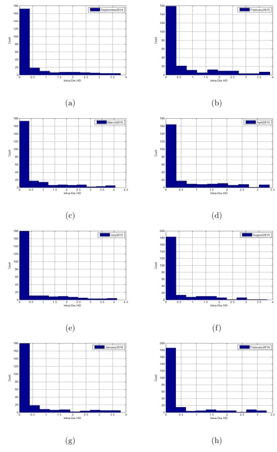
show the stability (percentages of ’1’s and ’0’s) across different set of measurements for DRAM1, DRAM2, DRAM3 respectively. . . 38 2.7 Distribution of Intra-die Hamming Distance (HD) among 48 (3×16)
DRAM-based PUFs under different operating conditions. . . 39
Different the extracted IDs. . . 44 2.9 Percentage of bit flips across multiple measurements (a) under
acceler-ated aging condition (Bit Selection Algorithm), (b) under random condition (Random Bit Selection) . . . 54
2.10 Percentages of HDs of DRAMs among different IDs under Aging condition
in (a) Sep. 2014, (b)Feb. 2015, (c) Mar. 2015, (d) Apr. 2015, (e) Jul.
2015 (f) Aug. 2015, (g) Jan. 2016, and (h) Feb. 2016. . . 58
3.1 DRAM cells array with a typical single MOSFET transistor and a storage capacitor. . . 66 3.2 Real data snippets that illustrate the DDR2 SDRAM operations: a)
Write. b) Delay(1). c) Read(1). d) Read(m). . . 67 3.3 Our DRAM Remanence based TRNG Model using MATLAB Curve
Fitting Tool (CFTool). . . 69 3.4 The histogram of the XORed data between Fluctuation and Startup
regions. . . 73 3.5 Scatter plot of percentage of ’1’s of XOR’ed data that are taken from
Fluctuation and Startup regions. . . 74
3.6 The histogram of the Uniqueness of the data at Fluctuation Region. . . . 75
3.7 Small section of the bitmap from DRAM for trial 3. . . 78
4.1 Histograms of a portion of the data (10000 samples) directly from six different power sources (Bench power supply, USB, Computer power source, DC power supply). . . 94 4.2 Input voltage plot of 1-second (240 samples) of the data from 6 different
power supplies. . . 95 4.3 Using voltage regulator (LT3501EFE#PBF) for plotting: (a)
His-togram of data (10000) samples, (b) Input voltage of 1-second (240 samples) of the data. . . 96 4.4 A schematic of our TRNG circuit design. . . 99 4.5 Plots of output voltage vs the number of samples while using (a)
1-inv, (b) 2-1-inv, (c)3-1-inv, and (d) 4-inv in chain using Monte Carlo simulation. . . 100 4.6 Percentages of 1’s at different input voltage level (0-5 volts) after using
different number of inverters in inverter chain (1-5 inverters) from 6 different power supplies. . . 105 4.7 DVFT circuit model for the proposed TRNG. . . 110 4.8 Timing diagram of different points (p0, p1, p2, p3) of our model. . . 113 4.9 Voltage sweeping using Arduino as a variable load to the input. . . . 121
5.2 A platform of IoT-based ubiquitous healthcare solutions using secure hardware elements for Authentication. . . 142 5.3 Security Approach for Low-Cost Verification of Devices and Patients
in the healthcare domain. . . 145 5.4 Schematic for key generation procedure. . . 150 5.5 Illustration of additional authentication methods to existing smart lock
model (Kwikset Kevo). . . 155
2.1 DRAMs Stability across Different Nominal Conditions . . . 29
2.2 Stability under Temperature Variations compared to Nominal Conditions . 30 2.3 Stability under Voltage Variations compared to Nominal Conditions . . . 31
2.4 Stability under Aging Condition compared to Nominal Conditions . . 33
2.5 Percentage of bit flips across multiple measurements (10-Sets) under Base-line (Base), Neighbor Selection (NS), Environmental Screening (ES), and combined (Algo) approaches. . . 40
2.6 Percentage of bit flips across multiple measurements under normal operating conditions. . . 40
2.7 Quality Evaluation of IDs from DRAM PUFs. . . 47
2.8 Stability of DRAMs due to Aging compare to Nominal Conditions . . 53
3.1 NIST Statistical Tests Results at Room Temperature Condition. . . . 76
3.2 DRAM trials and corresponding NIST tests . . . 82
3.3 DRAM trials with Von Neumann corrector . . . 84
3.4 DRAM trials XOR with Von Neumann corrector . . . 86
4.1 Power sources under evaluation . . . 98
TRNGs using different types of power supplies. . . 107 4.3 NIST Statistical Tests Suite average p-value results of our proposed
TRNG model using feedback loop (DVFT) implemented with dif-ferent power supplies. . . 122 4.4 NIST Statistical Tests Suite Results . . . 130
Introduction
As electronic devices become ubiquitous and more interconnected, people must depend on Integrated Circuits (ICs) for the security of sensitive information. Pro-viding this security relies on well-established primitives for key generation, data confidentiality and integrity, authentication, identification bit commitment, etc. Therefore, it is paramount for ICs to be able to perform operations and critical tasks in a low-cost yet highly secure way. Unfortunately, the conventional ap-proaches (e.g. digital signatures, encryption) suffer from various shortcomings; they are very slow, expensive, and increasingly vulnerable to physical and side channel attacks. Hardware-based security primitives such as physically unclon-able functions (PUFs) and true random number generators (TRNGs) can over-come these limitations and provide random functions in order to establish security and trustworthiness in critical application and systems. PUFs can derive secrets from the complex physical characteristics of ICs rather than storing the secrets in digital memories. PUFs can significantly increase physical security by generating
volatile secrets (keys) that only exist in a digital form when an IC is powered on and operating. Furthermore, a TRNG is an important security primitive used in a variety of applications including cryptographic algorithms, statistics, communi-cation systems, simulations, etc. It is critical that a TRNG be able to produce outputs consisting of fully unpredictable and unbiased bits in a cost-effective man-ner. In general, these hardware security primitives should provide low-cost and efficient trustworthiness of the physical hardware platforms. One should note that while these primitives can provide advantages to ICs, there are properties and details of the design that need to be considered (e.g. power usage, overhead, heat).
Since the Internet of Things (IoT) is a rapidly emerging paradigm, the most demanding requirement for their widespread realization is security. Apply-ing low-cost security solutions to a large scale of IoT [88] and even Cyber-Physical Systems (CPSs) [18] is possible using hardware-based security primitives such as PUFs and TRNGs. Providing a secure framework and platform for IoT systems can protect them against malicious attacks. One of the most challenging con-cerns for developing secure IoT devices is the resource constrained nature of these embedded systems. Security traditionally requires a great deal of resources in order to perform the computations necessary for encryption, certificate verifica-tion, third-party authenticaverifica-tion, etc. By implementing the previously discussed
hardware security primitives, developers can easily overcome the issues of resource constrained IoT device trustworthiness and verifiability in a low-cost and efficient way.
1.1 Security Vulnerabilities
In recent years, security has grown into a critical issue in modern information systems. Electronic hardware security, in particular, has emerged as one of the most serious challenges due to electronic devices penetrating every aspect of our society. Due to globalization trends, intellectual property (IP) vendors and system integrators have to deal with various counterfeiting issues more than ever and this surge in counterfeit hardware has driven the need for more secure chip authentica-tion. Among the sources of counterfeit chips are reintroduced discarded chips into the supply chain and fabrication of cheap copies that pass as authentic without significant scrutiny. Since the IP owner cannot be present during the fabrication process, this makes Integrated Circuit (IC) designs increasingly vulnerable to ma-licious modifications. In today’s technology-based day to day existence, there is a need to maintain the privacy of users and their data. These efforts are necessary to protect oneself against an unending tide of malicious activity and eavesdroppers. To complete this task one requires large random bit strings of information that can be applied for encoding, or decoding, sensitive information. The randomness
of the bit strings used allows a user to counter the ability of an attacker to predict the result of the data manipulation. Otherwise a nefarious individual would be able to decrypt secure communications with minimal effort due to function-based (e.g. time domain) knowledge. As a rule of thumb, the algorithms used to pro-duce these random numbers must have fast speed, require low power to operate, provide high reliability, and have high entropy.
1.2 Hardware Security Primitives
Traditional mathematical cryptography methods relies on the existence of one or more pieces of secret information (keys) to perform a secret exchange of infor-mation. The mathematical properties of the cryptographic algorithms ensure the infeasibility of mathematical attacks on the ciphers. However, these algorithms depend on the secure storage of these secret keys. With the ubiquitous deployment of cryptographic hardware and software secret storage of keys is not guaranteed because of the ability to easily attack non-volatile storage such as flash. Thus, alternative cryptographic protocols based on hardware security primitives that do not require an explicit secret key storage.
1.2.1 Physical Unclonable Functions
As a means to uniquely identify chips, researchers have proposed using the random process variations that naturally occur during the manufacturing process. These effects include process variations such as the size of transistors, capacitors, resis-tors and other components. These are unavoidable for the most part, and must be accounted during the design and layout process. However, these random process variations can be used to our advantage if we use them to generate unique intrin-sic identifiers. This is the idea behind Phyintrin-sically Unclonable Functions (PUFs), which was first proposed by Gassend et al. in 2002 [29]. Gassend and Pappu in 2001 developed the first silicon PUFs through the use of intrinsic process variation in deep submicron integrated circuits. They used the intrinsic process variability of silicon devices during manufacturing to produce unique, random and unclon-able digital responses and called it a physically random function. They have since been called physical unclonable function to emphasize the fact that they are not repeatable. Generally speaking, PUFs should present unpredictable, robust and unclonable characteristics. PUFs are circuits that have come into prominence in the past decade and hold much promise as a hardware security primitive.
A PUF can provide a hardware specific unique signature or a ”fingerprint” for an integrated circuit that can be leveraged for various security applications including authentication and secure access. One strong characteristic of a PUF is
that it can not be reverse engineered easily. There are two fundamental require-ments for building a PUF: random and uncontrollable variations. The variations must be random, thereby drastically reducing the probability that a unique sig-nature will be repeated. Also, the variations must be uncontrollable such that an adversary can not clone the devices. A PUFs inputs and outputs map a specific set of challenges to a set of corresponding responses which are called Challenge-Response Pairs (CRPs) [61]. In other words, a PUF is a multiple-input (chal-lenges) multiple-output (responses) function that has hard-to-predict dependency between the outputs and its inputs. The functional relationship between challenge and response looks like that of a random function. Because the PUF is derived from random process variation, it is very difficult, if not impossible, to predict the responses from a particular challenge or construct a function to do so in hardware or in software.
In general, a good PUF should have several parameters and characteristics, in particular Uniqueness, Reliability, and Randomness. Uniqueness of a PUF represents the ability of that PUF to uniquely generate responses. In other words, PUF uniqueness means that different PUFs generate different responses for the same challenge. Reliability of a PUF demonstrates that a given PUF can re-generate the same response for a particular challenge consistently. Finally, the randomness of a PUF indicates how random the response bits are. Ideally, the
response should follow a uniform distribution, whereby the proportion of 0s and 1s in the response bits should be equal. Figure 1.1 shows a PUF-based secure authentication technique. For simple IC authentication, PUF challenges (input) - response (output) pairs are collected from each chip, and stored in a secure database. In order to authenticate any given IC, one of the challenges is presented to the IC, the PUF embedded in the IC generates a response. If the produced response matches the one that is stored in the database, that means the IC is authentic. Note that in order to prevent man-in-the-middle (MiTM) attacks, each CRP (challenge-response pair) is used only once. An application for PUFs is that they can be used to provide secure, safe and low-cost authentication by generating unique secret keys/IDs. The ability of PUF devices to provide bit strings unique to each component can be leveraged as an authentication mechanism to detect tampering and attacks [16].
The advantage of using PUFs compared to traditional solutions is that they are: highly secure and inexpensive, because they provide volatile secrets which do not need to be stored anywhere and do not require any special fabrication technol-ogy and manufacturing process. Since PUF application is typically characterized by having two phases, enrollment and regeneration, it has the potential to be used for authentication purpose easily.
Fig. 1.1: Physical Unclonable Functions Secure Authentication Mechanism
1.2.2 Random Number Generations
Cryptography and security applications make extensive use of random numbers and random bits. Random numbers are useful for a variety of purposes, such as generating data encryption keys, simulating and modeling complex phenomena, selecting random samples from larger data sets, and even for gambling. Ran-dom number generators (RNGs) are classically divided into two different types: Pseudo random number generators (PRNGs) and True random number generators (TRNGs). PRNGs are deterministic in nature, but are traditionally adequate for most applications. These type of random number generators usually require a seed (i.e. number to initialize the internal state of the generator) and the seed should be periodically changed to keep the system secure. The number sequence produced by PRNGs is random within a specific time period; meaning the method of
ran-dom number generation does not provide truly ranran-dom behavior. TRNGs, on the other hand, derive their randomness from a physical entropy source and provide inherently nondeterministic behavior. They are unpredictable, and are random in the entire time domain. Since TRNGs are capable of producing uncorrelated and irreproducible procedures they act as a critical component within cryptographic systems and applications. For security-centric applications the high entropy num-bers from physical sources are a critical component in authentication and data encryption processes, where they are used to generate random cryptographic keys that are used to transmit data securely. Designing TRNGs around new forms of noise, one must account for certain features. Ideal TRNGs should display three essential characteristics: efficiency, non-determinism and non-periodicity. The dy-namically natured variations that are induced by power supply noise exhibit the necessary characteristics. A general schematic of a TRNG model is shown in 1.2. One can see that the model has a physical random source. There is also a data sampling module that can produce raw bits. If a user requires post-processing (e.g. Von Neumann [44]) then the model can produce processed data, at the cost of additional overhead to the model’s operation.
Noise Source Data Sampling Raw Data (random sequences) Post-processing Post processed random sequences Physical Segment of TRNG model Digital Segment of TRNG model
Fig. 1.2: General schematic of a TRNG model.
1.2.3 Security Primitives Potential Application Areas
Establishing security across physical hardware platforms can be a resource inten-sive and costly aspect when protecting the storage and exchange of data between components. As discussed in previous sections, one can use these security prim-itives for the purpose of securing physical objects to protect sensitive data and functionality of a device from a malicious actor. PUFs allow for unique identity to be attached to specific components or systems. This functionality provides the ability to authenticate hardware by producing individual signatures (IDs) for an implemented IC. It also can generate keys that can be used for encryp-tion/decryption algorithms. This is possible since the randomness of the produced IDs/keys are enough to be used for this purpose. As TRNGs are another security primitive that are uniquely tailored to produce high random sequences of bits for a
multitude of applications. These applications include: gaming, product labeling, simulations, cryptography and etc. The reason that these security primitives are widely adopted is they exploit the physical properties of a hardware system to produce random output. Due to this popularity, these solutions have the poten-tial to be used in securing IoT environments as long as their design is focused on being low-cost and resource efficient.
1.3 Problem Statement
Reliability and uniqueness are always important issues that hinders PUFs prac-tical applications. The stability of PUFs under various operating conditions has been a serious concern facing different kinds of PUFs. Another largest problems facing the continued use of hardware-based random functions (PUFs and RNGs) is that as technology continues to grow, there is a high demand for low-cost re-source efficient solutions. In order to overcome this potential future limitation, we proposed novel designs and architectures for the improvement of hardware-based random functions that meet the desired requirements of new embedded system security needs. Our solutions to this problem, which we will talk about in the following chapters, can be used to provide physical objects security in a variety of different applications such as the Internet of Things.
1.4 Related Works and Limitations
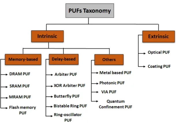
(1) PUFs: Since PUFs have gained considerable attention in the past few years, it
has yielded several proposed approaches for the realization of these functions. Fig-ure 1.3 shows a comprehensive taxonomy of existing PUF types and categorization. The two largest categories of PUFs are intrinsic and extrinsic. Extrinsic PUFs rely on some external stimuli in order to generate CRPs, for example light for an optical PUF. On the other hand, intrinsic PUFs are ones that depend on the nat-ural internal manufacturing property (process variation) of the device. Examples of intrinsic PUFs include delay based PUFs (arbiter PUF, RO PUF) which can depend on digital race condition or frequency oscillation (delay), respectively [40]. So far, various kinds of PUFs have been proposed for key generation/ID, such as RO-PUF [114], [60], [116], [111], [108], Arbiter PUF [94], Butterfly PUF [69], Clock PUF [113], Controlled PUF [20], Rowhammer PUF [90], Memristor PUF [68], etc. Many methods have already been proposed for identification and authentication of ICs such as in [94], [73]. Of particular interest are memory-based PUFs, which are attractive because most electronic systems have some type of memory included. The limitations of PUFs are that most previous PUF designs suffer from adding extra circuit to the existing hardware. However, memory-based PUF designs do not need any extra circuitry to achieve reliable PUF IDs/keys. Memory-based PUFs are usually based on the measurement of startup values of memory cells.
Fig. 1.3: PUFs Taxonomy based on Origin of Stimulus.
Flash memory is a Non-Volatile Memory (NVM) that has been proposed as a memory-based PUF in [102] and [77]. SRAM PUFs are one existing memory based PUF which has been presented in [106], [76], [91], [41], [42]. A SRAM PUF can generate a device-individual fingerprint using the startup behavior of its cells. SRAM PUFs exploit the inherent threshold variation of the cross-coupled SRAM cells. DRAM PUF is a newly presented work by Hashemian et al. [37], Keller et al. [52], Sutar et al. [95], Xiong et al. [107], Liu et al. [57]. Researchers have also proposed potential PUFs using future memory technologies such as memris-tors [86], [53], spintronic memories [43], MRAM-based PUFs [98], [21], etc.
(2) RNGs: Generally, PRNGs fit most of the application needs but there are demanding situations where PRNGs are substituted by TRNGs and those are the applications where it is important that the numbers be really unpredictable, such as for data encryption, and generating cryptographic keys. The reason be-ing the PRNGs lack of strong randomness properties [15], which can be seen via various statistical tests. Hence, the output sequences from TRNGs should have good statistical properties verified with the use of statistical tests, e.g. from NIST 800-22 statistical test suite [87]. However, the generation of true random bits is problematic in many practical applications of cryptography. Currently, several techniques are used for implementing TRNGs. In [12], Bruynincks et al. analyzed the security requirements of TRNGs, demonstrated the real-life attacks performed on various types of TRNGs and proposed solutions for generating safe cryptog-raphy random bits using TRNGs from untrusted vendors. In [104], the authors exploited random behavior from nearly-metastable operation of a group of FP-GAs. An oscillator-based TRNG has been proposed in [3] that can automatically adjusts the generated unbiased random numbers produced by process variation and dynamic temperature. Mudit et al. proposed a TRNG design based around sense amplifier circuits that are balanced in the metastable region using hot car-rier injection in [9]. Recently, new TRNG models such as Technology Independent (TI) TRNG, TRNG using hot-carrier injection balanced metastable sense
ampli-fiers, Portable TRNG for personal encryption application based on smart phone cameras, and Highly Efficient TRNG in FPGA Devices Using Phase-Locked Loops are investigated in [81], [9], [115], and [22], respectively.
Various types of TRNGs have been proposed using different noise and ran-dom sources such as ring oscillator (RO) TRNGs [24] [56] [82], memory based TRNGs such as flash memory based [102] [19], SRAM-based TRNG [79], block memory based TRNGs [33], metastability-based TRNGs [105], emerging device noise based TRNGs [17] [38], etc. Some hardware-based TRNGs use high gain amplifiers to enhance a noise source such that it can be discriminated by a com-parator [75], [2]. Burleson et al. did some analysis of on-chip true random number generators based on power supply variation [13].
The issue when examining the challenges of previous TRNG work is that there is a clear line of acceptance between a working TRNG and a non-working TRNG device. There is, however, a range of success for TRNG models that meet the required standard. Some TRNGs have better results in terms of randomness while others do not. The main challenge in TRNG research include low-cost design that are robust against manipulation of environments (voltage and temperature) and silicon aging. Our proposed TRNG models (DRAM remanence-based TRNG (chapter 3) and Power supply-noise based TRNG (chapter 4)) have the advan-tage of being very cost-effective and lightweight in terms of overhead. We have
proposed a remanence based TRNG that has the advantage of being simplistic, in that, our model does not need any extra hardware or overhead when compared to existing solutions for TRNGs. Furthermore, our power supply noise-based has the advantage of producing infinite number of random sequences.
1.5 Contributions
This thesis is devoted to the design and architecture of various hardware-based random number function security primitives that meets the requirements and needs for low-cost solutions in today’s electronic systems. Our work will also deal with the architectural requirements for designing resource efficient embedded system platforms. Specifically, our contributions are as follows:
1.5.1 PUF Design
We have developed new DRAM-based Physical Unclonable Functions using its startup value behavior. Furthermore, we evaluated silicon aging effects on DRAM PUFs reliability. Overall, developing PUF design for optimizing the use of existing hardware resources for the purpose of creating random output was our goal.
1.5.2 RNG Design
We have developed random number generators particularly TRNGs based on ex-isting memories (DRAM-based TRNG) and power supply-noise based true
ran-dom number generator. Our goal while working on RNG-related projects was to develop and introduce TRNG designs for the exploitation of the existing hardware platform characteristics to generate highly random bit streams.
1.5.3 Primitive Designs in IoT Environment
After producing improved designs of our hardware-based random functions and incredible results, we found that our developed solutions minimized additional cost overhead and made optimal use of system resources. We noticed that the majority of hardware-based random function solutions for distributed embedded systems environment (i.e. IoT) were not designed to be low-cost and resource efficient. We performed case studies to determine the effectiveness of our hardware security primitive solutions in IoT healthcare domain and smart device authentication (Smart DoorLock).
1.6 Thesis Outline
The outline of this thesis is as follows:
• Introduction
• DRAM-based Intrinsic Physically Unclonable Functions
• Power Supply Noise-based True Random Number Generation
• Hardware Security Architectures for the Internet of Things (IoT)
DRAM-based Intrinsic Physically Unclonable Functions
2.1 Introduction
In this chapter, we introduce an intrinsic PUF based on dynamic random access memories (DRAM). DRAM PUFs can be used in low cost identification appli-cations and also have several advantages over other PUFs such as large input patterns. The DRAM PUF relies on the fact that the capacitor in the DRAM initializes to random values at startup. We demonstrate real DRAM PUFs and describe an experimental setup to test different operating conditions on three DRAMs to achieve the highest reliable results. Furthermore, we select the most stable bits use as chip ID using our enrollment algorithm. We also evaluate silicon aging effects on DRAM PUFs in details. In other words, we explore the possibil-ity of intrinsic PUFs within Commercial Off-The-Shelf (COTS) DRAM ICs. We describe how to use the signatures to prevent modifications and uniquely identify and/or authenticate electronic devices.
2.2 Security Level Security
Most electronic systems are not designed with security in mind, as a result, there are always threats from attackers to alter these systems and leak secret informa-tion from them. Even if the systems are securely designed, there is no assurance that the delivered system is authentic. System level security mechanisms can use a subsystem on the board to prevent any altering or modification in system func-tionality and stop or reset system if any anomalous behavior has been detected. While it is difficult to authenticate the trustworthiness of any particular IC on a system board, a unique identifier, such as a PUF embedded in an IC can be used and gives the IC a unique identity. However, with COTS parts, a PUF or chip ID may not be available, so mechanisms for intrinsic PUF identification are needed. In this chapter, we present an intrinsic DRAM PUF that can be used to authenticate electronic systems on which DRAMs are present.
2.3 DRAM PUF Description and Properties
PUFs intrinsic to DRAM ICs have not been explored extensively. Our primary contribution is the identification of a DRAM PUF based on start up values. We examine the effect of various operating conditions such as temperature variation, voltage variation, and aging which may influence the behavior of the DRAM PUF. Finally, we propose a selection mechanism to isolate highly stable bits within the
large set of available bits in a DRAM.
2.3.1 DRAM PUF Advantages
DRAMs have some unique advantages that motivated us to explore it further:
1. Large input pattern: Because of the large number of available bits in a
typical DRAM, one can generate a large set of input challenges and cor-respondingly large output responses. This characteristic of DRAM PUF is very valuable which can make it to be distinct among all kinds of intrinsic PUFs.
2. Cost-effective: Since many computer systems have some form of DRAM
on board, DRAMs can be used as an effective system-level PUF as well. It is also much cheaper than SRAM. Thus, DRAM PUFs could be a source of random but reliable data for generating board identifications (chip ID). The advantage of the DRAM PUF is based on the fact that the stand-alone DRAM already present in a System on a Chip (SoC) can be used for generating device specific signatures without requiring any additional circuitry or hardware [37]. PUFs intrinsic to DRAM ICs have not been explored extensively. Ours is one of the first works in which a DRAM has been used as a system level security Physical Unclonable Function.
2.3.2 Potential DRAM PUF Implementations
DRAM memory cells are comprised of a paired transistor and capacitor. While ideally every DRAM cell should be identical, manufacturing imperfections cause slight physical variations in each cell. Moreover, every DRAM cell has its own physical trait. Therefore, the leakage effects on the storage nodes will vary as well. These physical variation characteristics can be potentially used to develop PUFs. The only previous work on DRAM PUF has been based on altering or disabling the refresh cycle [52]. Modern DRAM chips have a built in self-refresh module, as they not only require a power supply to retain data, but must also be periodically refreshed to prevent their data contents from fading away from the capacitors in their integrated circuits. The essential approach with refresh-based DRAM PUFs is to initialize all cells to 1 and then after some time, with refresh turned off, some of the cells will leak to 0. The randomness of which cells leak to 0 provide the opportunity for a PUF. The difficulty with using these refresh or retention based methods for a PUF is that it may take several minutes to hours for sufficient cells to flip to 0. Another potential approach is to use the remanence property of DRAMs. Contrary to popular belief, DRAMs can hold their values for surprisingly long intervals without power. DRAM cells retain their contents for a few seconds to minutes at room temperature. In fact, it has been demonstrated that sensitive information can be extracted from volatile memories due to data
remanence effects [31], [35]. Based on our examination on DRAMs, remanence approach is not feasible for constructing PUFs, however remanence effect can be used for creating True Random Number Generators (TRNGs).
2.3.3 Startup Value Based DRAM PUF
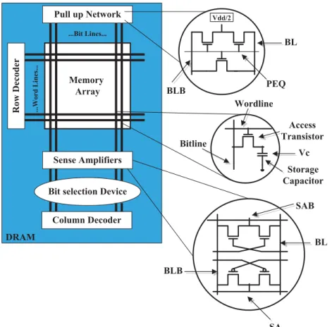
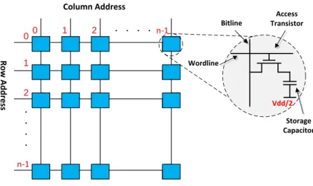
In our observation of DRAM refresh and remanence properties, however, we no-ticed that certain DRAMs actually exhibit behavior similar to SRAMs, i.e. they have seemingly random startup values. In other words, the cells do not initialize to ’0’ as would be expected. Thus, as with SRAMs, these startup values pro-vide a potential for creating a PUF. The reason for this random startup behavior can be explained by the interaction of precharge, row decoder, and column select lines when the device is powered up. Figure 2.1 shows the structure of a typical DRAM array. Bits are stored either by charging the storage capacitor to VDD or
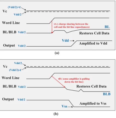
discharging it to ground. The timing diagram of the DRAM read operation of an uncharged cells is shown in Figure 2.2. In order to reduce the electric field stress on the capacitor, one of the plates of the capacitor is usually biased to
VDD
2 . Before the reading operation, the signal to precharge the bit lines (PEQ) is disabled. In normal operation, before reading the cell, the bitlines (BL and BLB) and sensing nodes (SA and SAB) are precharged to VDD
2 , and when the wordline is activated, the bitlines voltage will change slightly depending on the capacitance
of the storage capacitor. This slight change is detected by the sense amplifier as a ’1’ (Vdd) or ’0’ (Vss) as shown in Figure 2.2. In other words, the level of BL and BLB nodes eventually reaches the operating voltage (Vdd) or ground (Vss), respectively [45]. At startup, however, the storage capacitor has neither been charged to VDD nor discharged to ground. Thus, at startup, the nominal voltage
of each capacitor (Vc) is equal to the bias voltage VDD
2 which is equal to the bitline precharge voltage. Thus, when read, the sense amplifier is equally likely to read a ’1’ or ’0’. However, because of manufacturing variations, the storage capacitance of each bit will have slight differences, which leads to biasing of each bit to either a ’1’ or a ’0’. This behavior is what allows the startup values of the DRAM to function as a PUF.
2.3.4 Uniformity of Memory
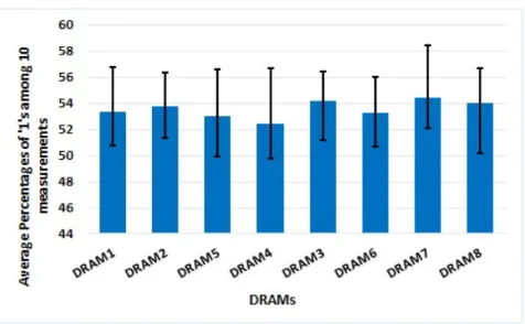
We start with an examination of the uniformity of a DRAM-based PUF. Ideally, 50% of the bits should be ’1’ and 50% should be ’0’. For each of the 8 DRAMs used for startup value experiments, we took 10 measurements of the uniformity -i.e. the percentage of bits that were ’1’ or ’0’ at startup. As shown in Figure 2.3, without any write operation to the DRAM cells, they have start up values and some of the cells values are one. While not perfectly uniform, the uniformity is close enough to ideal that with proper bit selection it can be used as a PUF. This
Storage Capacitor Access Transistor Wordline Bitline Memory Array Pull up Network Sense Amplifiers Column Decoder Row Decoder DRAM .. . Bit Lines ... ...Word Lines ... T Vdd/2
Bit selection Device
PEQ SAB SA BL BLB BL BLB Vc
Fig. 2.1: Memory structure of a One-Transistor DRAM array.
error bar shows the average, minimum and maximum percentage of ’1’ values of each DRAM (DRAM1 to DRAM8) across different trials. As an example for DRAM1, the average, minimum and maximum percentages of 1’s among all 10 measurements are 53.35%, 50.73% and 56.78%, respectively. As can be seen, there is a slight bias to ’1’ in all the DRAMs. Also, we looked at the distribution of 1’s within some of the DRAMs (DRAM1, DRAM2 and DRAM3) to make sure that they are not accumulated in some parts and saw that they are uniformly distributed across all the DRAM cells.
(a) (b) (Vdd/2)-ɛ Vc Vdd/2 Word Line Vdd/2
BL/BLB Restores Cell Data
BLB Vdd/2
Output
Amplified to Vss
Vss
tB ( sense amplifier is pulling down the bit line)
Vc Word Line Vdd/2 BL/BLB Vdd/2 Output Amplified to Vdd
Restores Cell Data
tA ( charge sharing between the cell and the bit line capacitances) Vdd/2
BL (Vdd/2)+ɛ
Vdd
Fig. 2.2: Timing diagram of a DRAM read operation of an uncharged cells biased
to Vdd (a) or Vss (b) due to process variations.
2.4 Experimental Setup
We used a set of 1-MBit HM51100AL CMOS DRAMs in DIP packages. Our setup essentially consists of four parts. Data acquisition experimental setup the FPGA based development board (Spartan 6 FPGA), the power supply & digital storage oscilloscope, the breadboard-based circuit (extension circuit), and the host PC. During data collection, the power supply supplies voltage to the extension circuit
Fig. 2.3: Uniformity of DRAMs across 10 measurements for each of 8 DRAMs (average percentages of 1s values)
(off-chip DRAMs) that is mounted on the breadboard and we check the voltage levels using the oscilloscope. The communication between the host PC and the FPGA is composed of two connections: USB connection which is used for FPGA configuration download. The other one is a high density serial connector which is used for data communication between the PC software, ISE Design Suit 14.7, and the software running on the FPGA (Developed using Xilinx EDK). In other words, The FPGA was programmed to control the test sequence supplied to the DRAM chip and transmit the outputs of the DRAM to a computer using an on-board USB-UART module.
2.5 DRAM PUF Evaluation under Different Environmental Operating Conditions
Here, we examine the stability of the DRAM PUF bits under various environmen-tal operating conditions. A stable bit is a bit that does not change in any trial and remains the same over different measurements of the same or different condi-tions. There are various parameters that can affect PUF stability such as process variation, PUF activity, temperature, supply voltage, etc. Others have proposed PUFs that take into account both process and environmental variations such as crosstalk which magnifies chip-to-chip signature randomness and uniqueness [100]. One of the advantages of our work is the stability evaluation against different op-erating conditions for more than one DRAM. We did all the experiments for three DRAMs which we will call them DRAM1, DRAM2 and DRAM3. We explore the differences between reliable and unreliable DRAM cell values, and the impact of operating conditions on them. To make a PUF highly reliable across its lifetime, unstable bits that are easily flipped by different operating conditions should not be used.
We start with baseline measurements (Nominal Condition (NC)) with the temperature set to 25◦C and the voltage to 5 V. For each DRAM, we took 10 measurements whereby we read all 1,048,576 (220) startup bits. The result from Table 2.1 shows that for DRAM1, 37.9% of the startup values were read as ’0’
across all 10 measurements and likewise 43.5% were read as ’1’ across all 10 measurements. Thus, 81.4% of the bits are marked stable, and the remaining 18.6% of bits, which read as both ’0’ and ’1’ on different measurements, are marked as unstable.
Table 2.1: DRAMs Stability across Different Nominal Conditions
DRAM1 DRAM2 DRAM3
Bit Value Bit Value Bit Value
0 1 0 1 0 1
37.9% 43.5% 27.9% 37.6% 26.6% 37.7%
81.4% 65.5% 64.3%
2.5.1 Stability of DRAM under Temperature Variation
We performed the experiments by sweeping the temperature from 0◦C to 80◦C using a ThemoStream system which is shown in Figure 2.4. In Table 2.2, we show the bit stability under both high temperature (80◦C) and low temperature (0◦C) conditions. NC-HT and NC-LT compare the stability of the DRAMs data under high temperature (HT) and low temperature (LT) conditions to the nominal condition (NC) stability, respectively - i.e. the percentage of nominal stable bits. In Table 2.2, stability means comparing a bit against the nominal condition. First, we derive the stable bits among the 10 measurements for each condition - i.e.
remain the same across all 10 measurements. Second, we find the stable bits among 10 measurements of the nominal condition. Finally, we identify which bits are stable across both sets of bits and the output provides the final stability results shown in Table 2.2.
Table 2.2: Stability under Temperature Variations compared to Nominal Conditions
DRAM1 DRAM2 DRAM3
% of stable bits % of stable bits % of stable bits
NC-HT 78.8% 64.4% 49.8%
NC-LT 49.9% 54.4% 44.3%
Fig. 2.4: Experimental setup with Xilinx Spartan-6 FPGA (right side) under
the test using the ThermoStream system for high and low temperature variations.
Table 2.3: Stability under Voltage Variations compared to Nominal Conditions
DRAM1 DRAM2 DRAM3
% of stable bits % of stable bits % of stable bits
NC-HV 55.4% 54.3% 30.5%
NC-LV 43.3% 26.7% 23.8%
2.5.2 Stability of DRAM PUF under Voltage Variation
We vary the nominal supply by 10% up and 10% down, and observe the PUF’s stability. Twenty measurements of startup values are taken at low voltage (4.5v) and high voltage (5.5v) (10 from each voltage). Table 2.3 contains the bit stability under both high and low voltage conditions for different DRAMs. Again, NC-HV and NC-LV compare the stability of the DRAMs data under high voltage (HV) and low temperature (LV) conditions to the nominal condition (NC) stability, respectively. As with temperature, we see that voltage variations can have an impact on the bit stability. The reason is because of the structure of a DRAM cell which consists of capacitor and a transistor. The startup values of a DRAM are dependent on the bias voltage of the capacitor, very slight variations in the power supply voltage can alter the voltage differential across the capacitor.
2.5.3 Stability of DRAM PUF due to Aging
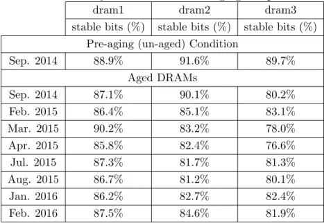
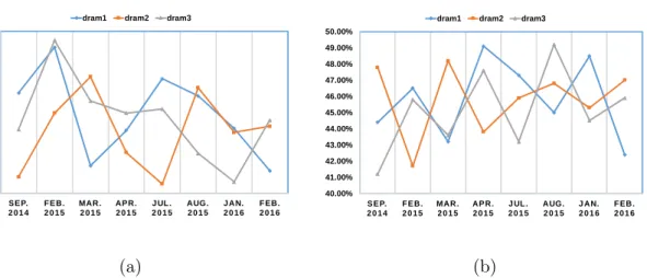
Finally, we explore the potential impact of aging on the stability of the DRAM PUF. Several aging mechanisms can affect reliability during the lifetime of an IC. VLSI phenomena such as bias temperature instability (BTI), hot carrier injec-tion (HCI), electro-migrainjec-tion and temperature-dependent dielectric breakdown (TDDB) are some of the causes of aging. As was mentioned in [101], among the BTIs, negative BTI (NBTI) affecting pMOS has more donating aging effect compared to positive BTI (PBTI) affecting nMOS. NBTI is enhanced by high temperature and high supply voltage. They both increase the threshold voltage and decrease the speed of CMOS transistors. A high switching rate in a circuit as well as excess supply voltage can enhance the HCI effect. A high operating voltage as well as higher temperatures can accelerate time-dependent dielectric breakdown (TDDB), a failure mechanism in MOSFETs.
In order to test the effects of aging on these DRAMs, we accelerated the aging process by performing in of the DRAM using the ThermoStream burn-in system. We did 8 hours of high-temperature agburn-ing at 80◦C to approximate the effects of 6 months of aging. In Table IV, NC-AA refers to the aging condition, and the table compares the stability of the aged DRAMs data to the nominal condition stability. The amount of stability degradation is not constant for each device. Table 2.4 shows that after aging still 71%, 65%, and 55.1% of the cells
remain stable after aging across different measurements for DRAM1, DRAM2, and DRAM3, respectively.
Table 2.4: Stability under Aging Condition compared to Nominal Conditions
DRAM1 DRAM2 DRAM3
% of stable bits % of stable bits % of stable bits
NC-AA 71% 65% 55.1%
2.6 Bit Selection Algorithm for Generating PUF IDs
Bit selection algorithm is an algorithm to select a set of bits for an ID/key that has a high likelihood of being stable [106]. The key insight of the algorithm is that we use spatial information within the DRAMs to infer the stability of a bit cell. We have a grid for memory rows and columns that can give us a very good picture of the cell distribution in the memory array. Thus, spatial correlations (neighborhood stable cells) can be made in both x and y directions. In all, the algorithm uses spatial information within the DRAMs to infer the stability of a bit cell. In other words, stable neighbors provides better reliability than random selection. The basic algorithm is shown in Algorithm 1. The DRAM is organized as an array of cells - in our case for a 1-MBit DRAM the array is 1024 rows by 1024 columns. We count the number of stable bits (ones and zeros) in each row and then select rows that have more stable bits than specific thresholds (T1 and
T2). Thresholds have been chosen based on experimentation in order to select 2048 bits (16 128-bits keys). In the ideal case, half will be zeros and half ones, among 1 MBit data in the next level of the algorithm. T1 and T2 are different in order to get the equal number of bits (ones and zeros) for the PUF ID bits. In fact, we have an algorithm to adjust the thresholds (T1 and T2). First we selected a random threshold value and then based on the number of 1s and 0s that have been selected, our algorithm can change the threshold value to upper or lower value in order to get 50% of ’1’s (1024 bits) and 50% of ’0’s (1024 bits). T1 and T2 are the thresholds for choosing rows that have more stable ’1’s and ’0’s, respectively. Among selected rows, those bits that have stable neighbors also identified as potential highly stable bits suitable for enrollment as the PUF ID/key. Note that T1 and T2 should be selected in a way to find almost equal number of ’1’s and ’0’s bits for the IDs.
As shown in Figure 2.5, the most stable bits have been selected considering the neighboring cells. Basically, it shows how to select the most stable and reliable bits from 1024 rows by 1024 columns grid for PUF ID considering neighborhood cell stability approach. The more the number of neighbors are stable around a cell, the more reliable the cell is. In Figure 2.5, the green cell at the center with value 1 has the best chance to be used as an ID bit since it has 8 neighbors which are all stable. Similarly, the white cell is not very suitable to be used as an ID bit
as it has several unstable neighbors around. We considered a 1024 by 1024 grid (rows and columns) on the memory cells. PUF ID bits have been selected from the bits that are stable among all the constraints (different operation conditions).
. . . . . Grid Columns 0-1023 G ri d R o w ss 0 -1 0 2 3 0 0 1023 1023 s PUF ID [128 bits] s s s 1 s s s s s u u s 1 s s u s
The most stable & reliable bit
(green)
C
B D ...
A ...
Fig. 2.5: Schematic of grids (rows and columns) on DRAM cells.
2.7 Analysis of Experimental Results and Their Validation
In the section, we first explain the multi-device evaluation on DRAMs based on different set of measurements, and then discuss the security metrics of uniqueness, randomness, and reliability followed by their results.
Algorithm 1 Highly Stable Bit Selection Algorithm for Selecting IDs from Different DRAM PUFs
1: Apply n measurements to each operating and environmental conditions including
Normal Conditions (NC), High Temperature (HT), Low Temperature (LT), High Voltage (HV), Low Voltage (LV).
2: Find bits that are stable across allnmeasurements of all conditions for the specific DRAM that has been enrolled (DRAM1 or DRAM2 or DRAM3). Note that we do not perform aging during enrollment because it is not practical to age the chip because of the time involved.
3: Count the number of stable bits (ones and zeros separately) in each DRAM cells
row.
4: Select rowsR that have more stable bits than selected thresholds (T1 for ’1’s and
T2 for ’0’s ) which have been selected based on experimentation in order to select
2048 (16 IDs) bits.
5: For each rowr∈R, enroll bits (r, j) that have a neighborhood of stable bits where
r is the row number and j is the column number. The neighborhood of stable bits
is defined such that row r−1 ∈R and r+ 1∈R and bits (r, j−1) and (r, j+ 1) are also stable.
2.7.1 Multi-device Evaluation on DRAMs
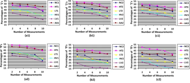
Here, we compare the results between DRAM1, DRAM2 and DRAM3. For each condition, we did 2-10 tests, collected data and the percentage of the stability among those data (for example for the high temperature condition, we had 2-10 different measurements). A bit is marked stable if it has the same result for all measurements. Figure 2.6 shows the percentages of 1s and 0s under different op-erational conditions and different set of measurements (2, 4, 6, 8, and 10) between DRAM1, DRAM2, and DRAM3. In most conditions, the degradation differences between the percentages of 2 measurements condition and 10 measurements are less than 10%. Figure 2.6 shows that by increasing the number of measurements, the percentage of stable bits, 1s and 0s (both of them) does not decrease very fast. Thus, most bits remain stable across multiple measurements.
2.7.2 Reliability
Reliability is a measure of repeatability or consistency with which a PUF generates its response across environmental variations, temperature, voltage, and aging. In our work, we chose stable bits based on the random selection and the proposed highly stable bit selection algorithm as discussed in the previous section. Vari-ous measurements from different operational conditions (HT, LT, etc) were used for each DRAM to apply bit selection algorithm on them. Then based on the
P e rc e n ta ge s o f ‘ 0 ’s 15 20 25 30 35 40 45 50 55 2 4 6 8 10 NC1 HT1 LT1 HV1 LV1 AA1 Number of Measurements 15 20 25 30 35 40 45 50 55 2 4 6 8 10 NC2 HT2 LT2 HV2 LV2 AA2 Number of Measurements P e rc e n ta ge s o f ‘ 1 ’s 15 20 25 30 35 40 45 50 55 2 4 6 8 10 NC3 HT3 LT3 HV3 LV3 AA3 Number of Measurements P e rc e n ta ge s o f ‘ 1 ’s 15 20 25 30 35 40 45 50 55 2 4 6 8 10 NC1 HT1 LT1 HV1 LV1 AA1 Number of Measurements P e rc e n ta ge s o f ‘ 1 ’s 15 20 25 30 35 40 45 50 55 2 4 6 8 10 NC2 HT2 LT2 HV2 LV2 AA2 Number of Measurements P e rc e n ta ge s o f ‘ 0 ’s 15 20 25 30 35 40 45 50 55 2 4 6 8 10 NC3 HT3 LT3 HV3 LV3 AA3 Number of Measurements P e rc e n ta ge s o f ‘ 0 ’s (a1) (a2) (b1) (b2) (c1) (c2)
Fig. 2.6: Muti-device evaluation; (a1) & (a2), (b1) & (b2), and (c1) & (c2)
show the stability (percentages of ’1’s and ’0’s) across different set of measurements for DRAM1, DRAM2, DRAM3 respectively.
number of distinct measurement approach (n=1 or n=2), we can determine which approach produced fewer bit flips during reconstruction phase. Our results show clearly that there is a relationship between better stability with bit selection and a higher number of distinct measurements (n), as shown in Table 2.5 and Table 2.6. We use Hamming Distance (HD) across different PUF measurements as the ba-sis of our metric. To estimate the reliability metric, an n-bit response (Ri) from
challenge C and from chip i should be extracted at normal operating condition (room temperature and normal supply voltage). The same challenge C is applied to chip i at a different operating condition to extract an n-bit response (Ri,2).
In the same way, T samples can be collected from chip i at different operating conditions. Hence, the average reliability metric (r) is estimated as:
ri = 1 T T X t=1 HD(Ri, Ri,t) n ×100% [63] (2.1)
where Ri,t is the t-th sample of Ri . The reliability metric shows the average
number of reliable PUF responses. Ideally, this value should be 0.
Fig. 2.7: Distribution of Intra-die Hamming Distance (HD) among 48 (3×16)
DRAM-based PUFs under different operating conditions.
For measuring intra-die HD, we consider 48 IDs (16 IDs associate with each DRAMs). Each ID has been compared with different measurements of every op-erating conditions such as (Nominal Condition, High Temperature, Low
Temper-Table 2.5: Percentage of bit flips across multiple measurements (10-Sets) under Base-line (Base), Neighbor Selection (NS), Environmental Screening (ES), and combined (Algo) approaches.
DRAM1 DRAM2 DRAM3
Base NS ES Algo Base NS ES Algo Base NS ES Algo
n=1 78.5% 13.5% 19.8% 13.8% 78.3% 20.6% 15.4% 13.5% 75.6% 18.3% 21.7% 10.4%
n=2 76.1% 8.7% 11.3% 3.8% 72.5% 13.5% 7.1% 7.7% 72.2% 14.4% 9.9% 8.8%
n=3 73.9% 6.6% 6.9% 2.3% 71.8% 7.6% 4.7% 3.1% 71.9% 8.5% 7.5% 3.8%
ature, High Voltage, Low Voltage, and Aging). Figure 2.7 shows the distribution of intra-die HD of 48 IDs from 3 DRAMs under various conditions. As it is shown, most of the IDs are stable under different conditions.
Table 2.6: Percentage of bit flips across multiple measurements under normal
oper-ating conditions.
DRAM1 DRAM2 DRAM3
BLine Algo BLine Algo BLine Algo
n=1 47.3% 2.1% 50.4% 2.3% 49.5% 3.1%
n=2 45.9% 1.5% 46.9% 1.4% 44.2% 1.7%
2.7.3 Our Selection Algorithm vs Baseline Algorithm
As indicated earlier, we used our selection algorithm to select 16 128-bit keys from the available bits and compared it to a naive baseline algorithm where 16 keys are selected at random from the 1-MBit set. In both cases, the enrollment is done based on either one, two, or three distinct measurements. In other words, n = 1, n = 2, or n = 3 for the algorithm in Algorithm 1. The baseline case only uses 1, 2, or 3 nominal case measurements, whereas our selection algorithm uses 5-15 measurements - 1, 2 or 3 each for NC, LV, HV
2.7.4 Uniqueness
We evaluate the uniqueness of the DRAM PUFs. In particular, Uniqueness means that the responses resulting from evaluating the same challenge on different PUF instances should not be similar. The uniqueness of a PUF circuit among a popula-tion of PUF circuits manufactured, depends on various factors such as the process variation of a particular manufacturing process, any manufacturing defects and the metric used to evaluate uniqueness. Inter-die HD can be used to evaluate the uniqueness of the PUFs data. It is typically used which averages the hamming distance between responses of various PUFs over multiple CRPs. Assume that there are k-chips and Ri and Rj are the n-bit responses to a challenge C from
and HT. Aging is not used for enrollment because of the time involved and since it also shortens the lifetime of the device. Since our algorithm is a combination of a neighborhood selection algorithm as well as screening due to environmen-tal measurements, we also evaluated each of these approaches separately. We evaluate the effectiveness of the selection algorithm by comparing the effect on reconstruction of the 16 keys. Ideally, on reconstruction we should read back the same bits. Table VI contains a summary of our PUF ID reconstruction results. Reconstruction consists of reading the keys back ten times under all conditions (NC, LV, HV, LT, HT and aging) - 60 reconstructions for each of the cases in the table. The data shows the number of bits that ipped in any of the reconstructions. As can be seen, the use of the enrollment algorithm (Algo) with just n = 1 - i.e. 5 measurements - reduces the number of bit ips for DRAM1 from nearly 79% in average for the baseline (Base) to less than 14%, which is sufficient for using the PUF for chip identification. In fact, our results show that we can also use this PUF for key generation with minimal ECC check bits. Furthermore, using more measurements during enrollment can decrease the number of bit ips signifi-cantly to 2-3%. It is interesting to note that while Neighborhood Selection (NS) and Environmental Selection (ES) are somewhat effective on their own, we get significantly better performance when both are used together (Algo). Note that Table VI is a worst case in that we examined the number of bit ips across multiple
measurements including under extreme operating conditions (40 measurements). Typically, however, reconstruction will be done under normal operating condi-tions. Table VII indicates the percentage of bit ips when reconstructing under just normal conditions. As can be seen, the bit ip rate is reduced to less than 3% with one set of measurements and to less than 1% with 3 sets of measurements.
Inter−dieHD= 2 k(k−1) k−1 X i=1 k X j=i+1 HD(Ri, Rj) n ×100% (2.2)
Ideally, the Hamming Distance (HD) between the responses should differ 50% of total responses bits.
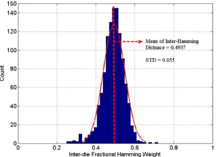
We calculated the average Inter-Hamming distance between all pairs of IDs that were extracted from the different PUFs (DRAM1, DRAM2 and DRAM3) based on our bit selection algorithm. Figure 2.8 shows the distribution of Inter-die HD of the 48 IDs from the 3 DRAMs. The average HD is 0.4937 and close to the ideal 0.5. Hence, the proposed DRAM PUFs can provide unique identifiers. As shown in Figure 2.8, the HD points tend to be very close to the mean of the set, as can be seen by the very small standard deviation of 0.055.
2.7.5 Randomness
In PUF design, the randomness of the data is very important as it can prevent the prediction of the cell values or the ID bits. In other words, perfectly random data
Fig. 2.8: Distribution of Inter-die Hamming Distance (HD) of 3 DRAMs among Different the extracted IDs.
means that the PUF cells are generated independently of each other, and the value of the next cell cannot be predicted, regardless of how many cells have already been produced. PUFs using intrinsic randomness are very attractive as they can be included in a design without applying any modifications to the manufacturing process. Note that if the HD uniqueness measure discussed above is 50%, it does not mean that data is necessarily random. To evaluate the Randomness of a PUF, statistical tests such as the NIST Test [87], Machine Learning (ML) techniques, Shannon entropy, or Min-entropy can be applied to the PUF data. Here, we considered Min-entropy as a metric to estimate the unpredictability (randomness) of our DRAM PUF data.
Min-entropy is an approach for estimating the randomness of the PUF re-sponses based on experimental data [54]. In particular, min-entropy indicates how many bits of a PUF response are uniformly random. In this literature, we esti-mate the entropy and min-entropy of the responses of all available PUFs. We have three DRAMs and for each of them, 16 IDs were selected based on the algorithm. Min-entropy is estimated as:
PM AX =M AX{Hwt(i),1−Hwt(i)} (2.3) Min-Entropy = 1 128 128 X i=1 (−log2(PM AX(i))) (2.4)
where i is the number of ID bits. First, we have to consider Hwt(i) for each bit over all IDs. In fact, the Hamming weight of a bit Hwt(i) is defined as the number of non-zero bits. The min-entropy that has been calculated based on Equation 1 which is 0.9483. This value is approximately close to the ideal case min-entropy of 1.
2.7.6 Case Studies
We evaluate security analysis such as reliability, uniqueness, and randomness for two different cases for ID extraction.
• Case1: Here, our goal is to find the maximum number of IDs using