04 August 2020
POLITECNICO DI TORINO
Repository ISTITUZIONALE
High Performance Computing via High Level Synthesis / Roozmeh, Mehdi. - (2018 Jul 06). Original
High Performance Computing via High Level Synthesis
Publisher:
Published
DOI:10.6092/polito/porto/2710706 Terms of use:
Altro tipo di accesso
Publisher copyright
(Article begins on next page)
This article is made available under terms and conditions as specified in the corresponding bibliographic description in the repository
Availability:
This version is available at: 11583/2710706 since: 2018-07-10T14:37:37Z Politecnico di Torino
High Performance Computing via
High Level Synthesis
Xilinx FPGA
By
Mehdi Roozmeh
******
Supervisor(s):
Prof. Luciano Lavagno
Doctoral Examination Committee:
Prof. Roberto Passerone , Referee, University of Trento Prof. Davide Quaglia, Referee, University of Verona Prof. E.F, University of...
Prof. G.H, University of... Prof. I.J, University of...
Politecnico di Torino 2018
Declaration
I hereby declare that, the contents and organization of this dissertation constitute my own original work and does not compromise in any way the rights of third parties, including those relating to the security of personal data.
Mehdi Roozmeh 2018
* This dissertation is presented in partial fulfillment of the requirements forPh.D. degreein the Graduate School of Politecnico di Torino (ScuDo).
Acknowledgements
First of all I appreciate the given opportunity to study and educate in Politecnico di Torino, during my PhD course in the Department of Electronics and Telecommunica-tions (DET) I met great and outstanding people which is impossible to name all, but I offer my sincerest gratitude to all who helped me to complete my study and find my future path.
Secondly, I would like to express my sincere gratitude to my advisor Prof. Luciano Lavagno for the continuous support of my Ph.D study and related research, for his patience, motivation, and immense knowledge. His guidance helped me in all the time of research and writing of this thesis. I could not have imagined having a better advisor and mentor for my PhD study.
Last but not least, my love goes to my parents and sister for the inspiration I draw from them during my life.
Mehdi Roozmeh 2018, Torino
As more and more powerful integrated circuits are appearing on the market, more and more applications, with very different requirements and workloads, are making use of the available computing power. This thesis is in particular devoted to High-Performance Computing applications, where those trends are carried to the extreme. In this domain, the primary aspects to be taken into consideration are (1) performance (by definition) and (2) energy consumption (since operational costs dominate over procurement costs). These requirements can be satisfied more easily by deploying heterogeneous platforms, which include CPUs, GPUs and FPGAs to provide a broad range of performance and energy-per-operation choices. In particular, as we will see, FPGAs clearly dominate both CPUs and GPUs in terms of energy, and can provide comparable performance.
An important aspect of this trend is of course design technology, because these applications were traditionally programmed in high-level languages, while FPGAs required low-level RTL design. The OpenCL(Open Computing Language) developed by the Khronos group enables developers to program CPU, GPU and recently FPGAs using functionally portable (but sadly not performance portable) source code which creates new possibilities and challenges both for research and industry1.
FPGAs have been always used for mid-size designs and ASIC prototyping thanks to their energy efficient and flexible hardware architecture, but their usage requires hardware design knowledge and laborious design cycles. Several approaches are developed and deployed to address this issue and shorten the gap between software and hardware in FPGA design flow, in order to enable FPGAs to capture a larger portion of the hardware acceleration market in datacenters. Moreover, FPGAs usage in data-centers is growing already, regardless of and in addition to their use as
1Both Intel and Xilinx provide software development kit(SDK) to support high level synthesis
vi
computational accelerators, because they can be used as high performance, low power and secure switches inside data-centers.
High-Level Synthesis (HLS) is the methodology that enables designers to map their applications on FPGAs (and ASICs). It synthesizes parallel hardware from a model originally written C-based programming languages .e.g. C/C++, SystemC and OpenCL. Design space exploration of the variety of implementations that can be obtained from this C model is possible through wide range of optimization techniques and directives, e.g. to pipeline loops and partition memories into multiple banks, which guide RTL generation toward application dependent hardware and benefit designers from flexible parallel architecture of FPGAs.
Model Based Design (MBD) is a high-level and visual process used to generate implementations that solve mathematical problems through a verified set of IP-blocks. MBD enables developers with different expertise, e.g. control theory, embedded software development, and hardware design to share a common design framework and contribute to a shared design using the same tool. Simulink, developed by Matlab, is a model based design tool for simulation and development of complex dynamical systems. Moreover, Simulink embedded code generators can produce verified C/C++ and HDL code from the graphical model. This code can be used to program micro-controllers and FPGAs. This PhD thesis work presents a study using automatic code generator of Simulink to target Xilinx FPGAs using both HDL and C/C++ code to demonstrate capabilities and challenges of high-level synthesis process. To do so, firstly, digital signal processing unit of a real-time radar application is developed using Simulink blocks. Secondly, generated C based model was used for high level synthesis process and finally the implementation cost of HLS is compared to traditional HDL synthesis using Xilinx tool chain.
Alternative to model based design approach, this work also presents an anal-ysis on FPGA programming via high-level synthesis techniques for computation-ally intensive algorithms and demonstrates the importance of HLS by comparing performance-per-watt of GPUs(NVIDIA) and FPGAs(Xilinx) manufactured in the same node running standard OpenCL benchmarks. We conclude that generation of high quality RTL from OpenCL model requires stronger hardware background with respect to the MBD approach, however, the availability of a fast and broad design space exploration ability and portability of the OpenCL code, e.g. to CPUs and GPUs, motivates FPGA industry leaders to provide users with OpenCL software
development environment which promises FPGA programming in CPU/GPU-like fashion. Our experiments, through extensive design space exploration(DSE), suggest that FPGAs have higher performance-per-watt with respect to two high-end GPUs manufactured in the same technology(28 nm). Moreover, FPGAs with more available resources and using a more modern process (20 nm) can outperform the tested GPUs while consuming much less power at the cost of more expensive devices.
Contents
List of Figures x
List of Tables xiii
1 FPGA - Field Programmable Gate Arrays 1
1.1 An example of a modern FPGA-based platform . . . 4
1.2 FPGA Architecture . . . 6
1.2.1 Configurable Logic Blocks . . . 6
1.2.2 DSP Slice . . . 8
1.2.3 Memory Resources . . . 9
1.3 HDL - Hardware Description Languages . . . 13
1.4 Contributions and Motivations: . . . 15
2 HLS - High Level Synthesis 17 2.1 State Of The Art . . . 17
2.2 High Level Synthesis and Model Based Design . . . 23
2.3 High Level Synthesis and OpenCL Model . . . 26
2.4 Xilinx SDAccel Development Environment . . . 28
2.4.1 Concepts of Application Host Code . . . 30
2.4.2 Static Region . . . 30
2.4.4 Off-chip to On-chip Interface Optimization . . . 33
2.4.5 On-chip optimization . . . 40
2.5 Design Space Exploration and HLS . . . 45
2.5.1 DSE of Multi-Core RTL via OpenCL Synthesis . . . 46
3 HPC - High Performance Computing 53 3.1 Platform and Underlying Hardware . . . 53
3.1.1 GPU . . . 54
3.1.2 High Bandwidth Memory(HBM): . . . 61
3.1.3 FPGA . . . 63
3.2 Applications . . . 63
3.2.1 Join Operation . . . 63
3.2.2 Frequency Modulated Continuous Wave (FMCW) Radar . . 72
4 Implementation and Performance-per-Watt Analysis of HPC Applica-tions on FPGA-GPU Platforms 79 4.1 FFT-based Digital Signal Processing Unit of Radar . . . 80
4.2 Implementation of a Performance Optimized Database Join Opera-tion on FPGA-GPU Platforms Using OpenCL . . . 85
4.2.1 Optimization of OpenCL models for FPGAs . . . 86
4.2.2 Power Analysis . . . 90
4.2.3 Performance-per-watt Analysis . . . 93
4.2.4 FPGAs and Energy Saving . . . 97
5 Conclusion 99
Bibliography 102
List of Figures
1.1 28 nm Xilinx Virtex7 FPGA . . . 1
1.2 Major share holders of FPGA market . . . 2
1.3 U.S. FPGA Market by application . . . 2
1.4 Asian Pacific FPGA Market by application . . . 3
1.5 Top view of data center . . . 4
1.6 Xilinx Ultrascale+ Platform Schem . . . 6
1.7 Top View of FPGA fabric architecture . . . 7
1.8 Slice of CLB . . . 8
1.9 Slice of DSP . . . 9
1.10 True Dual-Port Data Flows for a RAMB3 . . . 10
1.11 Comparison of 7 Series FPGA . . . 11
1.12 STRATIX® 10 FPGAs developed by Intel . . . 12
1.13 Graphical Presentation of full adder in different HDL level . . . 14
2.1 High level synthesis flow . . . 18
2.2 Scheduling and Binding . . . 20
2.3 Control Extraction and IO port Sequencing . . . 22
2.4 OpenCL platform and memory model . . . 26
2.5 SDAccel CPU/GPU-Like development environment . . . 28
2.7 Block Diagram of Example Xilinx SDAccel Platform . . . 31
2.8 SDAccel Recommended Flow . . . 33
2.9 Data-width Configuraion of Kintex7 CARD . . . 34
2.10 Memory Layout Matrix . . . 36
2.11 Device-Hardware-Transaction Timing Diagram . . . 38
2.12 Off-chip Memory With Two Separaeted Banks . . . 39
2.13 Device Hardware Transaction . . . 39
2.14 Loop Unrolling . . . 41
2.15 Array Partitioning . . . 43
2.16 Off-Chip bandwidth utilization vs on-chip memory size . . . 48
2.17 AXI memory controller diagram . . . 49
2.18 Design Space Exploration Flow of Multi Kernel OpenCL Models . . 50
2.19 Dynamic power consumption versus LUT utilization . . . 50
2.20 Quality of generated RTL by SDAccel for three kernels used in the sorting network . . . 51
3.1 Streaming Multi Processor of Kepler architecture . . . 57
3.2 Kepler Memory Hierarchy . . . 58
3.3 Streaming Maxwell’s Multiprocessors . . . 60
3.4 Stack of Memory Chips . . . 61
3.5 HBM . . . 62
3.6 Illustration of a simple sorting network . . . 66
3.7 Bitonic sort network with 8 inputs (N=8). It operates in 3 stages, it has a depth of 6 (steps) and employs 24 comparators. . . 67
3.8 Depth of Sorting network : D(N) =log2N.(log2N+1) 2 . . . 71
3.9 Number of Comparators :C(N) =N.log2N.(log2N+1) 4 . . . 71
3.10 FMCW radar signal analysis . . . 72
xii List of Figures
3.12 Estimation improvement by Interpolation . . . 73
3.13 Signal flow graph for radix-2, 8-point in place FFT computations . . 75
3.14 Signal flow graph for radix-2, 8-point FFT computations . . . 77
4.1 Operation of FMCW Doppler Radar . . . 80
4.2 FMCW Radar receiver architecture . . . 81
4.3 RTL simulation of FMCW model generated in ISE Simulator (ISim) 82 4.4 Timing diagram of streaming Simulink FFT from HDL library . . . 82
4.5 Comparison of synthesis result of streaming FFT IP using three different approaches . . . 83
4.6 HDL and C based design space exploration of FIR subsystem (LUT Utilization) . . . 84
4.7 HDL and C based design space exploration of FIR subsystem (FF Utilization) . . . 84
4.8 HDL and C based design space exploration of FIR subsystem (DSP Utilization) . . . 85
4.9 Memory model of single compute unit . . . 87
4.10 Fine-grained memory model of compute unit . . . 88
4.11 Top-level block diagram with 3 OpenCl kernel instances, generated by SDAccel. . . 89
4.12 Output of nvidia-smi dmon command line . . . 91
4.13 Vivado Power Analysis . . . 92
4.14 Tesla K80 Block Diagram . . . 94
4.15 Performance comparison of nested-loop join versus data size . . . . 95
4.16 Performance comparison of sort-merge join versus data size . . . . 95
1.1 7 Series FPGA Family comparison . . . 10
2.1 Loop Level Optimizations . . . 40
2.2 Array Optimization . . . 40
2.3 SDAccel off-chip to on-chip transfer analysis . . . 47
3.1 Release sequence of NVIDIA GPUs micro-architecture . . . 54
3.2 NVIDIA GPUs L1, L2 and register file size(Sizes are in KB) . . . . 58
3.3 Comparison of Kepler and Maxwell architecture . . . 59
3.4 Comparison of GDDR5 and HBM . . . 62
3.5 Computation Accuracy of FMCW RADAR . . . 74
3.6 Specification of Modeled FMCW Radar with FFT of 2048 . . . 74
4.1 FFT Implementation for Radar DSP Unit HLS-IP vs. HDL Coder . 81 4.2 Comparison of implementation cost for different radar blocks using HLS . . . 81
4.3 Full Radar DSP Unit Implementation HLS vs. HDL Coder . . . 81
4.4 Specification of tested Platforms . . . 93
4.5 Performance and energy analysis of Nested_Loop Join . . . 96
Chapter 1
FPGA - Field Programmable Gate
Arrays
Field programmable arrays(FPGA) consists of arrays of gates that can be pro-grammed and reconfigured by a designer. Hardware description languages (VHDL/Ver-ilog) are widely used to model a design in a bit and cycle accurate way and map them to FPGA via various available synthesis tools to generate functionally ver-ified bit-stream in an automated flow[1, 2]. Although, multiple companies share FPGA’s market, but Intel(after acquisition of Altera in 2016) and Xilinx are two major competitors. Even though Intel cannot be underestimated especially when it comes to their technology and capital, this work focuses on Xilinx tools and tech-nology. Xilinx is the market leaders of FPGAs with 18-months technology lead. Its products are aimed to meet requirements of various workloads coming from different domains[3, 4], figure1.2suggests that more than 50% of FPGA market belongs to Xilinx programmable platforms.
Figure 1.2 Major share holders of FPGA market
As technology world is shifting toward a huge ramp driven by 5G communi-cation, Artificial intelligence(AI) and Internet of Things(IoT), the demand of high performance computing and efficient-energy solutions are growing and this makes FPGA more suitable to be used as the core of embedded electronic systems. However, complexity of FPGA is growing day by day, but FPGAs development environment improvement in recent years made developers to consider them as a cost optimized and high performance devices, Figures1.3and1.4demonstrate increasing growth of FPGA deployment in USA and Asian pacific markets, overall annual market value of FPGA is estimated around 7 billion USD by the end of 2022 [5–7].
3
Figure 1.4 Asian Pacific FPGA Market by application, 2014-2024 (USD Bilion)
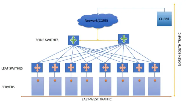
Moreover, previously most of the traffics in the INTERNET were between client and data-centers which is known as north-south traffic in data-center terminology, nowadays, 80 percent of the total traffic belongs to east-west traffic which is the internal communications within a data-center [8], figure1.5shows top view of data center architecture. This fact increases FPGA deployment in data centers mainly because of the FPGAs flexibility that can be configured as high-performance switches inside data centers structures without outside standards concern coming from client side[9].
Figure 1.5 Top view of Data center
In the rest of this chapter, FPGAs are discussed both from hardware and software perspective which are fundamentals to understand and perform successful software and hardware co-design targeting FPGAs.
1.1
An example of a modern FPGA-based platform
FPGAs, like any other integrated circuit, are mounted on boards (and often racks of boards) to create a complete electronic system. To give an idea of the power and pos-sibilities of modern FPGA-based platforms, we will consider a very recent example board, shown in figure1.6. HTG-9200 from HiTech Global is powered by the latest generation Xilinx Virtex Ultrascale+(16nm) FPGA. This modern platform is suitable, for example, for high performance optical networking applications since it has nine QSFP281ports and two separate DDR4 high-performance DRAM banks(using a total of 10 memory chips).
1Quad Small Form-Factor Pluggable is a high-performance and low-power Ethernet connectivity
solution for data center and high performance computing. These transceivers come in various types supporting 40 G and 100 G Ethernet.
1.1 An example of a modern FPGA-based platform 5
The HTG9200 is considerably more powerful than most FPGA boards that are deployed today. However, it is a clear example of an ongoing trend to replace ASICs with FPGAs for any application domain that require the latest technologies, but cannot afford to design an ASIC due to the Non-Recurrent Engineering cost. Design costs for the 14 nm technology node are estimated by various industry sources to be around 300M$ per design, and mask costs are most likely comparable. This means that several million integrated cicuits must be sold to recover the NRE costs. For this reason, and due to the ability to upgrade the hardware in situ, FPGAs are becoming the preferred platform for a growing number of applications, ranging from automotive (ADAS in particular), to telecom, military, aerospace, and recently even data centers. In the latter case, FPGAs are not competing with ASICs but with GPUs, and can offer comparable performance at a fraction of the energy-per computation cost, as we will show later in this thesis.
As we discussed, a key motivation of FPGAs is to keep design costs low. This is achieved first and foremost by reducing the verification costs dramatically, since their reprogrammability ensures that there is no need to get the first implementation completely bug-free. Designs can be reloaded at will, and debugging on the FPGA itself is much easier than on an ASIC.
Moreover, recent design technology advances, in particular High-Level Synthesis, have enabled a dramatic paradigm shift in terms of how FPGAs (and ASICs) are designed. As we will demonstrate in this thesis, HLS tools enable the designer to achieve high-quality implementations in a fraction of the time required by traditional HDL-based methodologies working at the Register Transfer level. The Quality of Results of RTL can even be surpassed by HLS-based solutions, thanks to the broader design space (e.g. the tradeoffs between pipelining and resource consumption, or the exploration of memory architectures) that is afforded by HLS. This motivates us to conduct an extensive research on different FPGA programming approaches and report our experiment results in this dissertation.
Figure 1.6 Xilinx Ultrascale+ Platform Scheme
1.2
FPGA Architecture
FPGAs are capable to serve as an accelerator for the wide range of applications ,moreover, new technologies shape and develop FPGA platforms day by day to meet customer and market needs. Modern FPGAs consist of millions of logic cells and switches which are programmable. This chapter studies the key components of FPGA chip and provide the numerical report of available resources for each component in 7 series Xilinx FPGAs(28 nm).
1.2.1
Configurable Logic Blocks
Figure1.7presents top view of FPGA fabric composed of arrays of configurable logic blocks(CLB) and switches.
1.2 FPGA Architecture 7
Figure 1.7 Top View of FPGA fabric architecture
CLBs are the key component in Xilinx FPGAs and each has pair of slices, figure1.8shows simplified graphical presentation of one slice with 6-input look-up tables(LUT), fast adders and registers. Logical,arithmetic,memory and shift register functions can be implemented using these slices [10].
Figure 1.8 Slice of CLB
1.2.2
DSP Slice
Xilinx FPGAs provide slices of DSP that are designed to implement vast number of binary multipliers and adders used in DSP applications. Figure1.9provides insight to DSP slice architecture used in 7series Xilinx FPGAs, implementation of DSP algorithms using DSP slices enhance speed and efficiency of FPGA device within a small size and flexible hardware [11].
1.2 FPGA Architecture 9
Figure 1.9 Slice of DSP
1.2.3
Memory Resources
Available on-chip memory is essential for high performance computing, however, LUTs in FPGAs can be used as distributed RAM across FPGA device, but dedicated blocks of RAM in FPGAs are the main resource of on-chip memory (fig1.10). Dual 36 Kb block RAM can be configured as a 64K x 1 (when cascaded with an adjacent 36 Kb block RAM),32K x 1, 16K x 2, 8K x 4, 4K x 9, 2K x 18, 1K x 36, or 512 x 72 in simple dual-port mode [12].
In order to address performance and power requirement of different applications, Xil-inx FPGAs are divided into three main families, table1.1reports available resources for each family member, however, they have similar architecture, but performance and power metrics of each device is different mainly because of available resource and external memory band-width.
Table 1.1 7 Series FPGA Family comparison
MAXIMUM CAPABILITY ARTIX KINTEX VIRTEX
LOGIC CELLS 215K 478K 1,955K
BLOCK RAM 13 Mb 34 Mb 68 Mb
DSP SLICES 740 1,920 3,600
MEMORY INTERFACE 1,066 Mbps 1,866 Mbs 1866 Mbps
Figure 1.10 True Dual-Port Data Flows for a RAMB36
Figure1.11draws a comparison between three family members of Xilinx, each can be deployed based on application requirements. VIRTEX with maximum number of logic cells is designed for high performance applications, while ARTIX provides users with low power devices, moreover, KINTEX devices are manufactured to offer best performance-per-cost FPGAs to designers.
1.2 FPGA Architecture 11
Figure 1.11 Comparison of 7 Series FPGA
INTEL FPGA Devices
However, Xilinx FPGAs are dominant in programmable logic market, but Altera FPGAs are also powerful devices with multiple classes that can offer costumers various performance, power and cost solutions to addressee different applications requirements. Additionally, reports in [13] suggest higher core performance of Intel FPGAs with respect to Xilinx UltraScale devices manufactured in 20 nm technology using ten different test bench targeting Intel and FPGA devices. Following lines briefly introduce five different FPGA classes produced by Intel which are currently closest competitor to Xilinx and may gain larger portion of FPGA market thanks to Intel investment and support[14].
STRATIX®
The Stratix® Series of FPGAs and SoC FPGAs are designed for the most demanding systems where performance is paramount. Stratix 10,figure 1.12 , is the flagship of Intel configurable device. Manufactured on Intel 14 nm Tri-Gate technology, Stratix 10 will offer industry-leading capacity, performance, and architectural innovation for the most challenging computing, signal-processing, and software-defined networking applications.
Figure 1.12 STRATIX® 10 FPGAs developed by Intel
Arria®
The Arria® Series of FPGAs and SoC FPGAs deliver abalance of performance
and power efficiency. Arria 10 FPGAs and SoC FPGAs are the latest product
within the Arria family. Arria 10 at 20 nm has a unique combination of speed, DSP performance, capacity and power efficiency, and are the only20 nmFPGA to integrate an embedded processor system.
MAX®
The MAX® Series of programmable logic devices features anon-volatile ar-chitecture and offers alow cost and low power configurable logics. MAX devices are widely used forgeneral-purpose and power-sensitivedesigns in a wide variety of market segments to perform functions that include I/O expansion, interface
bridging, power management, and FPGA configuration control.
Cyclone®
The Cyclone® Series of FPGAs and SoC FPGAs are optimized forlow-cost, high-volume systems. Cyclone V deliver capacity, performance, and IP ideal for the majority of embedded applications used in theindustrial and automotive markets.
1.3 HDL - Hardware Description Languages 13
Enpirion®
The Enpirion® product line offers the industry’smost compact, energy-efficient, and sophisticated DC-DC convertersfor meeting the power requirements of FP-GAs. When power rails demand programmableon/off, fast transient response and extra-low noisedevices they are the winner candidate.
1.3
HDL - Hardware Description Languages
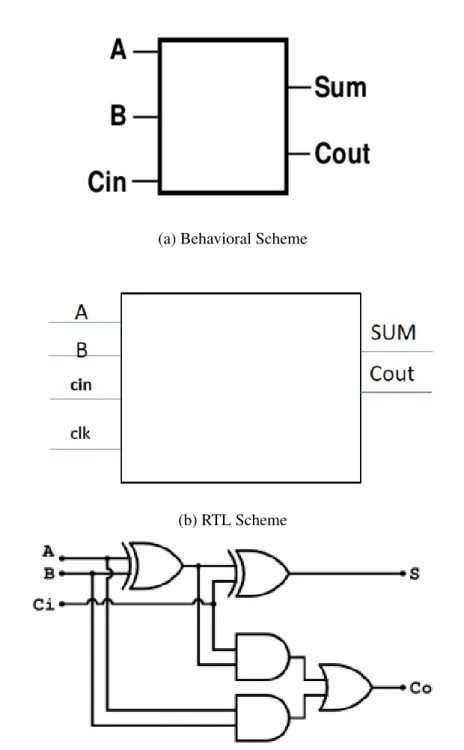
Hardware Description Language(HDL) is used to model digital electronic system, in other words, any digital electronic component such as registers, memories and switches can be modeled in HDL. VHDL/Verilog are common HDL languages in industry which support designing at three main levels of abstraction, although, designing digital electronic circuits can be done both using top-down and bottom-up approach, but the latter method is almost obsolete because of modern digital circuit complexity. Three different levels of HDL are shown in figure1.13and described below.
• Behavioral Level: enable hardware designers to model whole algorithm start-ing from top level, each block consists of sequential function and tasks with defined inputs and outputs. In this level designers are focused on behavior and performance of the algorithm and only when behavioral level is verified, designers can develop underlying digital circuits of algorithm using register transfer level abstraction.
• Register-Transfer Level (RTL): In this level designers can model digital circuits at resister level using cycle accurate timing. Technically, RTL code can be used by synthesis tools in order to generate gate-level model from algorithm. • Gate Level: The lowest level of abstraction is gate level which can be used to implement digital algorithm on silicon after placement and routing stage which can be done automatically by modern synthesis tools.
(a) Behavioral Scheme
(b) RTL Scheme
(c) Gate Level Presentation
1.4 Contributions and Motivations: 15
1.4
Contributions and Motivations:
The rest of this dissertation presents a study on the high-level synthesis (HLS) methodology for high performance computing applications (HPC) using two differ-ent approaches. To do so, firstly, this work discusses high-level synthesis, Model Based Design (MBD) and parallel computing that helps to provide the necessary background for analyzing the conducted experiments in this work. The main motiva-tion behind this study relies on the importance of high performance and low power hardware to address the ever-growing demand for energy efficient platforms. Hence, the experiments are designed to examine Xilinx high-level synthesis tool chain in an analytical manner using various type of C based model (e.g. C, SystemC and OpenCL) for DSP and data base applications.
As the first stage of this PhD course, Simulink is used to develop a real-time application of digital signal processing unit of frequency modulated continuous wave (FMCW) radar. The top level model is used to generate functionality verified C and HDL based model in customizable fashion. Thereupon, the Xilinx synthesis tool chain is used to map automatic generated codes on FPGAs. Although, the results suggest that C based FPGA programming consumes less resources for performing the same amount of computation, performance hungry part of the DSP algorithm is substituted with SystemC IP that can be integrated within Simulink environment and be used to realize parallel RTL. The results of this study are discussed in more detail in chapters three, four and [15].
The growing trend towards heterogeneous platforms is crucial to meet time and power consumption constraints for high-performance computing applications. The OpenCL parallel programming language and framework enable programming CPU, GPU and recently FPGAs using the same source code. This eases software developers to implement applications on various devices supported by heterogeneous HPC platforms. This work presents two very different FPGA implementations of a database join operation, one using a direct O(n2) algorithm, and the other using a bitonic sort network to speed up the join operation. Comparison of performance and energy consumption for both FPGA and GPUs is provided which suggests an average of 40% performance-per-watt improvement by using an FPGA instead of a GPU. Extensive analysis and discussions related to these experiments are presented in chapters two, three and [16, 17]
Even though, MBD offers faster development cycle with respect to code based model due to early stage verification and coarse-grained subsystem integration, the available design space is much larger in latter case thanks to low level exposure capabilities. This leads the quest for the best implementation towards design space exploration (DSE) analysis of OpenCL models. The proposed DSE technique, discussed in the next chapter and demonstrated in the chapter four, offers careful design space exploration by considering on-chip and off-chip sources of parallelism. Additionally, power estimation based on the area utilization enables exploration of design space at a faster pace.
Chapter 2
HLS - High Level Synthesis
Technically speaking, High Level Synthesis(HLS) is automated flow which trans-forms C based model algorithm to register transfer level (RTL) that can be used to program FPGAs. Current Xilinx HLS tools chain supports C/C++, systemC and OpenCL as source code and generates high quality RTL based on design constraints and optimization directives provided by a designer [18, 19].
2.1
State Of The Art
Design complexity of electronic devices is growing day by day and manufactur-ing optimized hardware requires strong technology and knowledge to address the need of wide range of computational intensive workloads such as artificial intel-ligence(AI) and digital signal processing applications. Companies like Intel and NVIDIA manufacture parallel fixed-architecture GPUs which can be programmed by software developers using parallel programming languages such as OpenCL and CUDA. Moreover, the growing trend toward hybrid platform is crucial to meet time and power constraints of ever-evolving high performance computing applications.
Recent studies suggest that FPGAs have performance and power consumption advantage over GPUs thanks to technology advancement in FPGA manufacturing and development environment improvement which shortened the gap between hardware and software layer[20, 17]. Algorithms can be developed and verified at system level within the same frame work as CPU/GPU, this automated flow and FPGAs inherent reconfigurable parallel architecture result in high performance and low
power hardware which can be tuned and adopted according to design constraints during design cycles (figure2.1).
Figure 2.1 High level synthesis flow
High level synthesis enables designers with minimum hardware experience to program modern FPGAs through sophisticated tool chain that supports application development for FPGA starting from pure software level. Next section covers high level synthesis principles and optimization techniques which are used in this work to generate desirable RTL micro-architecture from higher abstraction layer.
2.1 State Of The Art 19
High Level Synthesis Principles:
In this part of the thesis techniques and terminologies of Xilinx tool chain are explained using user manual and optimization instructions. The codes and fig-ures are derived from Xilinx documentation which are prepared to introduce their product in a most advantageous form. However, each section refer to re-lated document, it would be helpful to mention that the information of the rest of this section are obtained from [21–25].
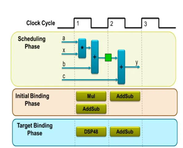
Scheduling and binding are the processes at the heart of high level synthesis. The code below is used to explain theses process [24].
int foo(char x, char a, char b, char c) { char y;
y = x*a+b+c; return y }
Scheduling: Scheduling is the process that HLS decides in which clock cycle operations should occur. This depends on the clock frequency, timing information of the target FPGA , and any additional optimization directives.
Binding:In this stage of high level synthesis, the tool determines which hardware resources implement each scheduled operation.
The scheduling phase section of figure2.2depicts this step. The multiplication and the first addition are performed in the first clock cycle. The next clock cycle executes the second addition. The green square in this figure indicates when an on-chip memory is written. The maximum number of scheduled operation in one clock cycle depends upon the clock period and the operation execution time. Faster FPGA can complete all above computations in one clock cycle, conversely, slower FPGAs may take more clock cycles.
Figure 2.2 Scheduling and Binding
Specific information about FPGA target device is needed to decide which re-source is the most optimized solution for each implementation. Multiplication and addition can be implemented by DSP48 resource which is the high performance and power-efficient unit in FPGA architecture [24].
2.1 State Of The Art 21
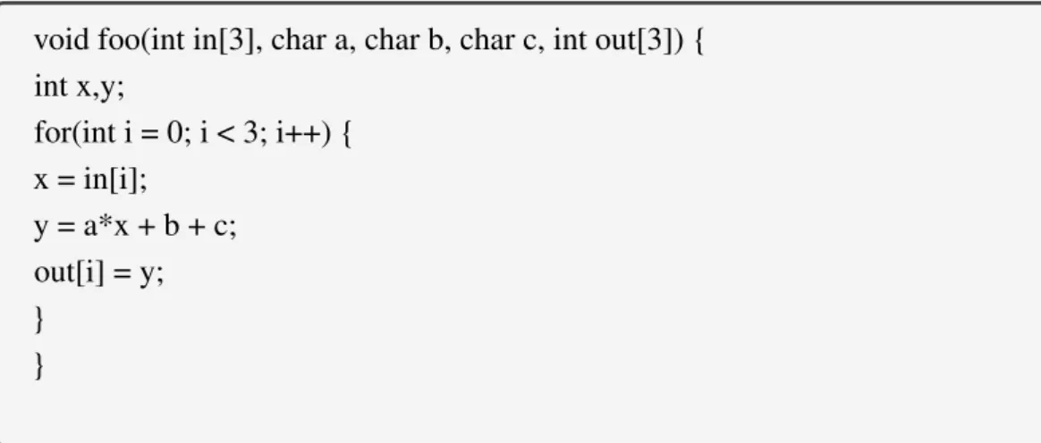
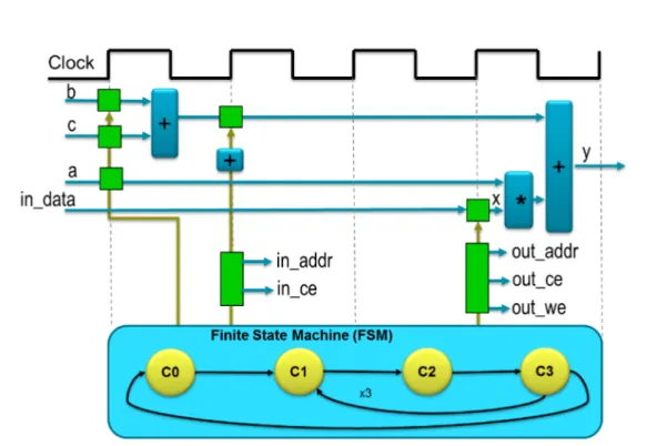
Final step of high level synthesis is extraction and implementation of control logic and I/O ports. The simple C code below is used to clarify this process with more details. Generated RTL by HLS runs the logics inside the loop three times, high level synthesis tools produces a Finite State Machine (FSM) in the hardware design to complete these operations.
void foo(int in[3], char a, char b, char c, int out[3]) { int x,y; for(int i = 0; i < 3; i++) { x = in[i]; y = a*x + b + c; out[i] = y; } }
Figure2.3illustrates final scheduled design and generated FSM by HLS which is described below in more details.
• The C0 is the first state of FSM which is followed by C1, C2 and C3. The full sequence of states are :C0,{C1, C2, C3} ,{C1,C2,C3},{C1,C2,C3} , C0. • The variables only once require the addition of theb andc. This operation
pulls outside the (for-)loop and performed in the stateC0. Each time the design enters stateC3it reuses the operation result.
• The data for in is returned from the block-RAM in state C2 and stored as variablex.
• The data from portais read with other values to perform the calculation. The firstyoutput is generated and the FSM ensures that the correct address and control signals are generated to store this value outside the block.
• The design then returns to stateC1to read the next value from the array/block-RAMin.
• The design then returns to stateC0to read the next values ofbandcto start the process all over again.
2.2 High Level Synthesis and Model Based Design 23
2.2
High Level Synthesis and Model Based Design
Model Based Design environments (MBDEs), such as Simulink, are becoming more widespread as they expand their capabilities of synthesizing efficient hardware and software from high-level algorithmic models. They find applications in very important areas such as digital signal processing (DSP), telecommunications, and control systems. MBDEs allow modeling of complex algorithms and systems at a very abstract level, using pre-defined primitive micro and macro blocks (e.g. adders, multipliers, multiplexers, FIR filters, FFTs). The designer can thus focus on defining the best algorithm without caring for tedious low level implementation details. Such details can be introduced later in the design flow via automated model-to-model translation, including both direct mapping and sophisticated hardware and software synthesis algorithms, or through a user-directed refinement process.
One of the major advantages of MBD tools is that they let the designer verify and validate abstract golden models against their design specifications. The designer can then use these models to generate code targeting either a specific embedded processor for software implementation, or a register transfer level (RTL) descrip-tion for hardware synthesis. The process of generating software code or the RTL hardware description is normally assisted by the designer by providing constraints and directives. Algorithmic design provides a much better scope for power, area and performance optimizations as compared to what can be achieved at lower lev-els. MBD also greatly eases the verification task by allowing one to re-use already verified macro blocks and more importantly by letting the designer use the same verified golden reference model throughout the complete design, verification and implementation flow.
State of the art MBD tools used in the industry can generate very efficient and optimized software code for different target processors, by using information about the target processor architecture. But hardware implementation essentially entails the generation of a cycle accurate RTL model from very abstract block level models that have no notion of clock cycles. Hence the set of choices is much broader, and the normal direct translation strategy used for software implementation is likely to fail. Current MBD tools, such as Simulink from the Mathworks, can generate a very limited set of hardware implementations starting from a given model. In other words, they have limited capabilities to explore the hardware design space starting from a single model, due to reasons that are described more with detail in the next sections.
This is particularly true in the case of complex blocks like a Fast Fourier Transform (FFT), a Discrete Cosine Transform (DCT) or a Viterbi decoder, which are normally represented as Simulink macro blocks.
Simulink models can be also translated to RTL description for hardware synthesis through a tool called HDL Coder. Efficient hardware implementation starting from an abstract model generally requires effective design space exploration (DSE) from a single model. HDL Coder, however, has limited capabilities in this regard, especially when it comes to complex algorithms like FFT, DCT, and Viterbi decoders. Each HDL coder block is mapped to a few micro-architectures, e.g. fully sequential and fully pipelined, which provide only a few design points, such as minimum area or maximum throughput. Many of the architectural trade-offs that are essential for optimized hardware implementation, such as independent definition or throughput and latency, or the choice of memory parallelism and architecture, may even need to be performed manually, by changing the source model every time. This changing of model defies one of the main purposes of model-based design, by requiring different models for different implementations, and hence making the design process long and tedious.
Simulink has a rich library of components that can be used to model systems and algorithms from many different domains. In Simulink libraries, the components are arranged in groups known as blocksets, for example the DSP-blockset that can be used to model DSP algorithms. Simulink libraries are extensible through a mechanism known as S-functions. It provides a component modeling paradigm in which the functionality (algorithm) as well as the interaction with other components can be represented in a well-defined way. The S-functions can be written in C, FORTRAN, or MATLAB, as required.
Simulink comes integrated with a tool called Real Time Workshop (RTW). RTW is a set of code generators known as target language compilers (TLC) that can trans-late a Simulink model to C/C++. Each TLC can be optimized to generate code for a different processor or platform. Embedded Real Time (ERT) coder is one of these TLCs, which is optimized to generate software code for embedded applications. It can generate floating and fixed point code. Part of this work presents a study on high level synthesis and the legacy code generated by RTW and HDL coder which can be divided into three main sections:
2.2 High Level Synthesis and Model Based Design 25
1. Modeling and validation of digital signal processing unit of specific type of RADAR used in automotive industry via Simulink which will be described in chapter 3.
2. Generation of SystemC-based FFT IP with fully pipelined stages to be substi-tuted with Simulink C model. The data flow and analysis of FFT algorithms are explained in chapter3.
3. Comparison of high level and RTL synthesis using HDL and C-based Simulink IPs is reported in chapter 4.
Alternative to model based design approach, in the next section, new program-ming framework is discussed that can target heterogeneous platforms equipped with CPU, GPU and FPGA devices. OpenCL(Open Computing Language) is sup-ported by industry leaders to program various hardware accelerators within the same framework using close-to metal optimization options.
2.3
High Level Synthesis and OpenCL Model
The OpenCL Programming model has been developed by the Khronos group to overcome the hurdles of programming multi-core and heterogeneous compute plat-forms. OpenCL enables programmers to develop both close-to-the metal and portable software. Although, OpenCL is a high-level programming language, it provides a low-level abstraction layer that can expose significant architectural aspects of the target hardware, such as massive parallelism and the memory hierarchy. The CPU/GPU based platforms generally have a fixed architecture. While this makes programming easier and compilation times much faster, it is also a limitation because it reduces both the energy efficiency and the on-chip ("local" in OpenCL terms) memory access bandwidth with respect to an FPGA.
Figure 2.4 OpenCL platform and memory model
An OpenCL device consists of compute units (CU), each further divided into processing elements (PE) as shown in Fig 2.4. Several concurrent executions of the kernel body (called work-items) take place on multiple processing elements. The work-items are further grouped into work-groups, which are being executed by compute units. The memory is broadly divided into host (i.e. CPU) memory and device (i.e. GPU or FPGA) memory. The device memory is further divided into private memory (specific to each work-item), local mem- ory (shared by all the items in a group) and a global/constant memory (shared by all the work-groups). Access to global memory is the slowest (since it typically resides in external
2.3 High Level Synthesis and OpenCL Model 27
DRAM) while private memory is the fastest (since it is typically allocated to register files), while local memory often resides in on-chip SRAM. Global memory however, is the largest in size while private memory is the smallest. The OpenCL memory model is also shown in figure2.4. The work-items that compose an OpenCL kernel can be executed in an out-of order manner, in order to ensure high performance on a variety of platforms with different numbers of CUs [26]. Thus, the OpenCL standard uses a three-level synchronization and collaboration model. The execution order of different kernels is completely determined by the host code, either by calling them sequentially, or by using synchronization callbacks that notify the host code when a given kernel has completed execution. The execution of different work-groups within a kernel is completely unsynchronized, thus they must read and write different areas of global memory, and they cannot cooperate in any manner. Finally, the programmer can use explicit barriers to ensure local and global memory consistency for items within a group.A barrier represents a checkpoint within a work-group. All the work-items belonging to that work-group must reach it before any of them can proceed beyond it.
2.4
Xilinx SDAccel Development Environment
The new Xilinx SDAccel™ Development Environment provides high performance application developers the dedicated FPGA-based hardware and software tool chain. SDAccel offers a fast, micro and macro architecture optimized compiler that makes efficient use of on-chip FPGA resources; a well-known software-development flow with an Eclipse™-based Integrated Design Environment (IDE) for software develop-ment, profiling, and verification, which provides a CPU/GPU-like work environment; and dynamic reconfigurable accelerators optimized for different high performance applications that can be swapped in and out on the fly for a CPU/GPU-like run-time environment[22, 27].
Figure 2.5 SDAccel CPU/GPU-Like development environment
OpenCL defines hierarchical memory model that is common between all vendors and can be applied to all OpenCL applications. Global, local and private memories are the main layers of this hierarchy. SDAccel maps them to the FPGA platform as external DRAMs, BRAMs, and register. SDAccel allows even finer-grained exploitation of the on-chip memory architecture of FPGAs by using directives such as on-chip global memory, multiple AXI buses for kernel global arrays, and partitioned local arrays, which enable a designer to finetune the memory architecture
2.4 Xilinx SDAccel Development Environment 29
and adapt the RTL architecture to the application, rather than the application to the GPU architecture[16].
The Xilinx® SDAccel OpenCL boards are PCIe® based accelerator cards that plug into a standard PCIe slot in x86_64 host or server type architectures.
Figure 2.6 Programmable Device Block Diagram
The Xilinx PCIe hardware device consists of two regions, as shown in figure 2.6, the Static Region and the Programmable Region. The Static Region provides the connectivity framework to the Programmable Region, which will execute the hardware functions as defined in the software kernel. The diagram above is an example of a standard partial reconfiguration hardware platform. The expanded partial reconfiguration hardware platform would incorporate most of the static region into the programmable region [28].
The rest of this chapter is dedicated to fundamental concepts of host , static and programmable region of FPGA based platform and demonstrate how Xilinx FPGA device can be programmed in CPU/GPU-like environment using SDAccel tool chain.
2.4.1
Concepts of Application Host Code
In OpenCL framework, hostcode is responsible for manging the platform of acceler-ator mainly by performing following steps:
• Platform setup
• Allocate and transfer buffers to the device • Run accelerator
• Read buffers from device memory
OpenCL programs are normally compiled completely at runtime which are handled by the host code APIs. Although, writing a proper host code for single or multiple kernels which can also act as test-bench will take considerable amount of time and programming effort, but application developers use template host codes and apply modifications based on algorithm requirements. Our group in Politecnico di Torino developed various design examples with different host codes for database applications for single and multiple kernels which are documented in public github repository and can be accessed byhttps://github.com/HLSpolito.
2.4.2
Static Region
In programmable device terminology, static region is containing all the necessary logics for implementation ofrequired interface between host, compute units and off-chip global memory. This static region is a pre-defined base platform that can be flashed onto an EPROM on the board. The FPGA would then be programmed with this base platform upon power-up. As shown in Figure2.7, communication between DDR, host and reconfigurable OpenCL region is performed through static region.
2.4 Xilinx SDAccel Development Environment 31
Figure 2.7 Block Diagram of Example Xilinx SDAccel Platform
2.4.3
Programmable Region
The programmable region contains the programmable section of the device that accepts the software kernel from the SDAccel tool chain. Implementation of compu-tation intensive part of algorithm is done by optimizing and directing synthesis flow of OpenCL kernel using a wide range of provided directives by SDAccel. According to SDAccel terminology, area and performance optimization of the design falls into three main categories:
1. Host Code optimization
2. off-chip to on-chip interface optimization 3. On-chip optimization
In the following parts of this chapter, these categories are described in detail to discuss how one OpenCL source code can be implemented on FPGA with different power and performance characteristics using SDAccel development environment. To achieve the highest possible performance on FPGA these optimizations are paramount since the OpenCL standard guarantees functional portability but not performance portability.
Optimizing for an FPGA using the SDAccel tool chain requires the same effort as code optimization for a CPU/GPU. The one difference in optimization for these platforms is that in a CPU/GPU, the programmer is trying to get the best mapping of an application onto a fixed architecture. For an FPGA, the programmer is concerned with guiding the compiler to generate optimized compute architecture for each accelerator (referred to as a kernel) in the application.
As specified by the OpenCL standard, any code that complies with the OpenCL specification is functionally portable and will execute on any computing platform that supports the standard. Therefore, any code changes are for performance optimization. To aid the user in these optimizations, SDAccel offers performance profiling capabil-ities integrated into the run-time. This profiling helps the user analyze the achieved performance and pinpoint any potential bottlenecks that need to be addressed.
The SDAccel™ Environment is a complete software development environment for creating, compiling, and optimizing OpenCL™ applications to be accelerated on Xilinx® FPGAs. Figure2.8 shows the recommended flow for optimizing an application in the SDAccel Environment [22].
2.4 Xilinx SDAccel Development Environment 33
Figure 2.8 SDAccel Recommended Flow
2.4.4
Off-chip to On-chip Interface Optimization
In the OpenCL™ programming model, all data are transferred from the host memory to the global memory on the device first and then from the global memory to the kernel for computation. The computation results are written back from the kernel to the global memory and lastly from the global memory to the host memory. How data can be efficiently moved around in this programming model is a key factor for
determining strategies for kernel computation optimization, so it is recommended to optimize the data movement in your application before taking on optimizing the computation.
During data movement optimization, it is important to isolate data transfer code from computation code because inefficiency in computation may cause stalls in data movement. Xilinx recommends that you modify the host code and kernels with data transfer code only for this optimization step. The goal is to maximize the system level data throughput by maximizing PCIe bandwidth utilization and DDR bandwidth utilization. It usually takes multiple iterations of running CPU emulation, hardware emulation, as well as execution on FPGAs to achieve the goal.
Efficient data movement between the kernel running in the FPGA and external global memory is critical to the performance of acceleration applications. There is an inherent latency overhead to read and write data from external DDR SDRAM. A well-designed kernel minimizes this latency impact and maximizes the usage of the available data bandwidth provided by the acceleration platform.
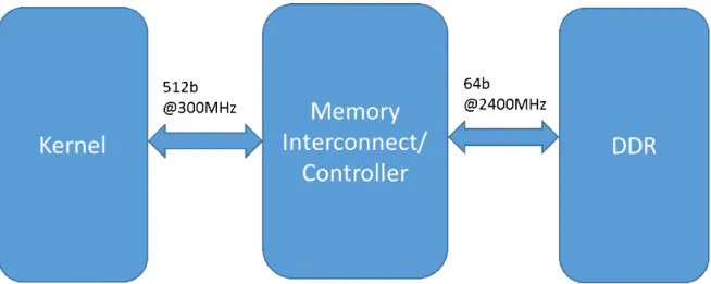
SDAccel Environment includes a variety of FPGA acceleration cards with differ-ent DDR memory configurations. The figure below shows the data path between a kernel and one of 4 DDR channels on the XIL-ACCEL-RD-KU115 card. Each DDR channel provides 20GB/s raw DDR bandwidth with 80GB/s total for the entire card.
2.4 Xilinx SDAccel Development Environment 35
The width of the data path between the kernel and the memory interconnect/con-troller can configured by the SDAccel compiler as 32, 64, 128, 256, and 512 bits depending on the kernel argument types. For applications that require maximum data bandwidth between the kernel and DDR memory it is recommended that global pointers are defined explicitly as 512-bit data types.
OpenCL C specification defines vector data types that can have up to 16 elements of the same basic C data type. Kernel arguments defined as int16, uint16, and
float16 are automatically packed by the SDAccel compiler as 512-bit interfaces during synthesis.
Below is the code usinguint16data type that directs synthesis toward wide mem-ory interface between kernel and off-chip global memmem-ory. A 512-bit AXI4 memmem-ory mapped interface will be generated for these global pointers after compilation [25].
kernel __attribute__ ((reqd_work_group_size(1, 1, 1))) void vadd(
const __global uint16 *in1, // Read-Only Vector 1 const __global uint16 *in2, // Read-Only Vector 2 __global uint16 *out, // Output Result
int size // Size in integer )
{
KERNEL BODY
Inferring Burst Transfer from/to Global Memory:
The most common global memories used on Xilinx® acceleration cards are DDR3 and DDR4 SDRAMs. They are most efficient when operated in burst mode. In addition there are overheads associated with switching between DDR read and write. Xilinx recommends to transfer large amount of data in a single burst to achieve the best efficiency of the memory controller and keep the compute unit inside the FPGA device busy all the time.
The memory layout of data objects is a key factor to consider for improving the data transfer efficiency. Considering a 4x4 matrix “a” example, conceptually it is a two dimensional array as shown in the matrix logical layout in the Figure below. In C/C++ programming, arrays are physically stored in row-major order that all data within a row are stored in consecutive locations followed by the data within the next row as shown in the matrix physical layout below. The implication is that if your algorithm reads the data column-wise, the burst transfer will not happen as it reads from discrete location each time. This can generally be optimized by either transposing your data in the host code or caching multiple columns of data in the kernel [25].
2.4 Xilinx SDAccel Development Environment 37
Figure2.10depicts physical layout of memory access pattern on FPGA device that can be read from/to in burst fashion. Below is the code that suggests proper coding style for performing burst read for one dimensional vectors.
kernel __attribute__ ((reqd_work_group_size(1, 1, 1))) void vadd(
const __global uint16 *in1, // Read-Only Vector 1 const __global uint16 *in2, // Read-Only Vector 2 __global uint16 *out, // Output Result
int size // Size in integer )
{
local uint16 v1_local[LOCAL_MEM_SIZE]; // Local memory to store vector1
int size_in16 = (size-1) / VECTOR_SIZE + 1; ...
for(int i = 0; i < size_in16; i += LOCAL_MEM_SIZE) {
...
int chunk_size = LOCAL_MEM_SIZE; //boundary checks
if ((i + LOCAL_MEM_SIZE) > size_in16) chunk_size = size_in16 - i;
v1_rd: __attribute__((xcl_pipeline_loop)) for (int j = 0 ; j < chunk_size; j++){ v1_local[j] = in1 [i + j];
} ... } }
The Device Hardware Transaction view below shows that multiple read bursts are sent at the kernel start and all read data come back continuously after the memory read latency.
Figure 2.11 Device-Hardware-Transaction Timing Diagram
Using Multiple DDR Banks:
For applications demanding high bandwidth to the global memory, devices with multiple DDR banks can be targeted so that kernels can access all available memory banks simultaneously. For example, SDAccel™ includes platforms that support multiple DDR banks which is supported by Xilinx® vendor extension. Creation of multiple AXI4 interfaces are necessary to assign multiple DDR bank to each kernel which can be done both from host code or inside OpenCL kernel. Figure2.12depicts high level representation of two BANK implementation of OpenCL source code.
2.4 Xilinx SDAccel Development Environment 39
Figure 2.12 Off-chip memory with two separated Banks
Figure2.13shows transaction of off-chip memory with on-chip AXI interface using two separate DDR banks. Read and write operations are performed separately and in parallel which result in improvement of overall bandwidth utilization [25].
2.4.5
On-chip optimization
Interface optimization is crucial and the first step of RTL optimization. After high speed interface synthesis that transfer data between on-chip and off-chip section of FPGA platform with maximum possible efficiency, data is processed on-chip in pipelined and parallel fashion. This requires to tailor and direct compilation flow of OpenCL and C/C++ kernel toward parallel and pipelined hardware using wide range of provided directives by Xilinx HLS tool. Table2.1and Table2.2list array and loop-level optimization directives in Xilinx high level synthesis tool which this work provides overall review over them. For additional information on other optimization techniques and how they can be implemented using Xilinx high level synthesis tools it is suggested to refer to provided user-guide by Xilinx [22, 24].
Table 2.1 Loop Level Optimizations
Unrolling Unroll for-loops to create multiple independent operations Merging Merge consecutive loops to reduce overall latency, Flattening Allows nested loops to be collapsed into a single loop Dataflow Allows sequential loops to operate concurrently
Pipelining Used to increase throughput by performing concurrent operations Tripcount Provides user override of iteration analysis
Latency Specify a cycle latency for the loop operation
Table 2.2 Array Optimization
Resource Specify which hardware resource (RAM component) an array maps to
Map Reconfigures array dimensions
Partition Partitioned into multiple smaller arrays
Reshape Reshape an array from one with many elements to one with greater word-width Stream Specifies that an array should be implemented as a FIFO rather than RAM.
2.4 Xilinx SDAccel Development Environment 41
Unrolling Loops
By default loops are kept rolled in High-Level Synthesis. That is to say that the loops are treated as a single entity: all operations in the loop are implemented using the same hardware resources for iteration of the loop. Below is the code with simple for loop that perform multiplication between array b and c and store results in array a. Figure2.14shows presentation of three different hardware solutions for the same source code [24].
Figure 2.14 Loop Unrolling
• Rolled Loop: When the loop is rolled, each iteration will be performed in a separate clock cycle. This implementation takes four clock cycles, only requires one multiplier and each RAM can be a single port RAM.
• Partially Unrolled Loop: In this example, the loop is partially unrolled by a factor of 2. This implementation required two multipliers and dual-port RAMs to support two reads or writes to each RAM in the same clock cycle. This implementation does however only take 2 clock cycles to complete: twice the throughput and half the latency of the rolled loop version
• Unrolled loop: In the fully unrolled version the entire loop operation can be performed in a single clock cycle. This implementation however requires four multipliers. More importantly, this implementation requires the ability to perform 4 read and 4 write operations in the same clock cycle. Since quad-port RAMs are not common, this implementation may require the arrays be implemented as registers rather than RAMs.
Array partitioning
The message below is the common problem when pipeline directive is used. This issue avoid proper pipelining of generated hardware withinitiation interval(II) of onewhich means successive iteration of a loop can not be executed next after each other with minimum latency [24].
@I[SCHED-61] Pipelining loop ’SUM_LOOP’.
@W [SCHED-69] Unable to schedule ’load’ operation (’mem_load_2’, bottleneck.c:57) on array ’mem’ due to limited memory ports.
@I[SCHED-61] Pipelining result: Target II: 1, Final II: 2, Depth: 3.
Arrays access conflicts usually cause this kind of problem. Implementation of arrays as block-RAM with maximum of two data ports can limit the throughput of a read/write operations within the loop.
Arrays are partitioned using the ARRAY_PARTITION directives in order to in-crease available memory port and overall bandwidth utilization.Vivado HLS enables designers to partition on-chip memory in three different styles as shown in figure 2.15and described below .
• Block:The original array is split into equally sized blocks of consecutive elements of the original array.
• Cyclic:The original array is split into equally sized blocks interleaving the elements of the original array.
2.4 Xilinx SDAccel Development Environment 43
• Complete: The default operation is to split the array into its individual elements. This corresponds to resolving a memory into registers.
Figure 2.15 Array Partitioning
Array Mapping
Small arrays in source code can be mapped into a single larger array by map directive which usually reduces the number of required block-RAM [24].
The ARRAY_MAP directive supports two ways of mapping small arrays into a larger one:
• Horizontal mapping: This corresponds to creating a new array by concate-nating the original arrays. Physically, this gets implemented as asingle array with more elements. This option is useful to increaseresource sharing and
minimizing power consumption.
• Vertical mapping: This corresponds to creating a new array by concatenating the original words in the array. Physically, this gets implemented by a single
array with a larger bit-width. This option is useful to increase memory bandwidth.
2.5 Design Space Exploration and HLS 45
2.5
Design Space Exploration and HLS
It has been a long endeavor and evolution in Electronic-System-Level design industry to generate and optimized automatic RTL from C-based description, nowadays, generation of high quality RTL for industrial purpose is possible thanks to modern HLS tool [29–31], more importantly, available directives such as loop unrolling, memory partitioning and multiple instantiation of compute kernels1(multi-core) enable designers to perform broad and in-depth design space exploration(DSE) to realize application driven hardware. In fact, fine and coarse-grained parallelism of generated RTL are feasible by directing the compilation flow of C-based model using customizable optimization options provided by modern HLS tools to drive optimum solution with highest performance-per-watt.
The rest of this work covers design space exploration of related work to ex-plain the orientations and approaches of previous HLS based DSE. Afterwards, the author proposes an automated DSE flow for multi core OpenCL based FPGA implementation which provides design hints based on Xilinx HLS output.
Various DSE approaches are studied and proposed in literature. A Pre-RTL power-performance simulator, called Aladdin, is proposed in [32] which enables rapid design space exploration of accelerator with high accuracy in the early stage of design. Author in [33] suggests that careful exploration of all solutions can result in area efficiency by proper partitioning of multidimensional arrays and unrolling nested-loops to reduce the area over head caused by bank switching. Automated DSE flow is proposed in [31] to obtain Pareto-optimal curve (performance versus area) of the application mapped on FPGA using HLS methodology, similarly, HLS-based DSE approach is discussed in [34] based on user defined area and time constraint which suggests the best RTL solution based on the design requirements. HLS enables designer to select the bit-width of variables from behavioral description, author in [35] describes a method to perform DSE for FPGA by controlling the amount of resource sharing using automatic bit-width controller of HLS tool. Parallel and multi-threaded method for finding the optimum micro-architecture for a given SystemC model is presented in [36], the author suggests a DSE flow to minimize the size of design for a given target latency.
As HLS tools are becoming more mature, the demand of C-based IPs are increas-ing. Synthesizable C-based IPs require DSE at micro-architectural level, author in [37, 38] presents automated flow to perform design space exploration on generated C models from Simulink IP block sets which shields a designer to understand legacy code and obtains a set of Pareto-optimal solutions based on defined constraints, addi-tionally, macro-architectural trade-offs are considered by wrapping different parts of the C-model into SystemC version to derive parallel RTL from behavioral description of Simulink model via HLS. Study in [39] presents a learning-based method for DSE that eases and accelerates micro-architectural modification using Random-Forest model which considers all different knobs (micro-architectural choice) and number of possible choices(e.g. unrolling and partitioning factor) to select Pareto-optimal solution for final RTL realization.
However, important aspects of on-chip DSE are discussed at above-mentioned works, but efficient data transfer from off-chip to on-chip memory is a design neces-sity to drive high performance RTL. Interestingly, architectural template is proposed in [40] that is capable to consider off-chip source of parallelism in deep convolutional neural networks in which author claims generated RTL has better performance in comparison to previous works using identical neural networks targeting same FPGA devices.
In the next section, we propose a design space exploration method considering area, power and execution time of each OpenCL kernel among set of candidate solutions. Our experiment suggests, reported in chapter four, our best RTL on Xilinx Virtex7 has higher performance-per-watt with respect to two different high-end GPUs manufactured in the same node (28 nm). Moreover, our golden solution can outperform tested GPUs by using Xilinx UltraScale FPGAs (20 nm) at the cost of more expensive devices with much larger available on-chip resources.
2.5.1
DSE of Multi-Core RTL via OpenCL Synthesis
In order to sift through design alternatives prior to implementation, analyzing perfor-mance and efficiency of off-chip to on-chip memory transfers is crucial. To do so, we introduce the following parameters and monitor memory interface performance using different configurations. Table2.3reports the memory interface performance
2.5 Design Space Exploration and HLS 47
of the generated RTL by SDAccel for burst and normal memory transfers.
Number of Transfers (NT): Number of total independent transfers between DDR and kernel. Each transfer sends a pack of data with the specified burst size for read or write operations.
Burst Size (BS): The data size of each transfer. The maximum burst size is assumed to be 4096 bytes [23].
Transfer Efficiency (TE %): Burst size / Maximum Burst size.
Transfer Rate (MB/s): (Total Transfer (MB) / Total Transfer time (s) )
Bandwidth Utilization (BW%): (Transfer Rate / Available Bandwidth2)
Table 2.3 SDAccel off-chip to on-chip transfer analysis
NT BS TE BW MB Time(ms)
Burst 32 1024 25% 6.8% .032768 .049
Non-Burst 8192 64 1.56% 61% .524288 .088
Figure. 2.16plots bandwidth utilization versus on-chip memory size. The non-burst memory configuration has low transfer efficiency, which increases the overall execution time of the kernel. In the second scenario, the memory controller is using burst access which increases transfer efficiency. Note that the total transfered data is much higher in the second row which explains why the transfer efficiency is different with respect to the burst mode. The results are important since they demonstrate the effect of local size on memory controller performance using available IPs for on-chip to off-chip interface.
Figure 2.16 Off-Chip bandwidth utilization vs on-chip memory size
The results of this section are obtained only by performing read and write op-erations to evaluate the performance of memory controller by isolating on-chip computation from off-chip transfers. The remaining memory bandwidth could be used, for example, to increase the computational power of the FPGA, by instantiating multiple parallel compute units (OpenCL work-groups).
Algorithm1describes the design space exploration method used in this work. The algorithm below, illustrated in Figure. 2.18, suggests an automated flow which considers area utilization, execution time and total number of work-groups for each solution and suggests the minimum required numbers of compute-unit to meet the given time constraint. Figure. 2.20shows the output of DSE flow for each kernel used in the sorting network. The bitonic-sorting algorithm is composed of three different kernels each with different off-chip memory access pattern and internal computations. In fact, each solution is a RTL core with a unique optimization
setting synthesized from the OpenCL WGs. The solution with lowest energy
consumption that meets resource and performance constraint is chosen for imple-mentation of each kernel on the target FPGA.
The proposed algorithm estimates the quality of each solution considering three main criteria described below:
2.5 Design Space Exploration and HLS 49
Figure 2.17 AXI memory controller diagram
1. Execution time of each compute unite obtained from cycle accurate RTL sim-ulation. The performance of each RTL core , generated from OpenCL WG, depends on off-chip bandwidth utilization and on-chip data path optimization.
time[i][j]; i∈ {1. . .Solution}, j∈ {1. . .Kernels}
2. Design area of each solution that also reflects dynamic power consumption of the kernel. Figure. 2.19illustrates the semi-linear relation between LUT utilization on a Virtex7 device and dynamic power consumption for the three kernels used in the bitonic-sort algorithm.
LU T[i][j]; i∈ {1. . .Solution}, j∈ {1. . .Kernels}
3. Total number of required compute units to complete computation which de-pends on the local size of the OpenCL kernel and may decrease the perfor-mance of the device due to inefficient usage of the memory controller3.
The main motivation behind developing this routine is to estimate the relative quality of all solutions with