University of Windsor University of Windsor
Scholarship at UWindsor
Scholarship at UWindsor
Electronic Theses and Dissertations Theses, Dissertations, and Major Papers
11-17-2019
FPGA-Based Acceleration of the Self-Organizing Map (SOM)
FPGA-Based Acceleration of the Self-Organizing Map (SOM)
Algorithm using High-Level Synthesis
Algorithm using High-Level Synthesis
Mohammad Abdul Moin Oninda University of Windsor
Follow this and additional works at: https://scholar.uwindsor.ca/etd
Recommended Citation Recommended Citation
Oninda, Mohammad Abdul Moin, "FPGA-Based Acceleration of the Self-Organizing Map (SOM) Algorithm using High-Level Synthesis" (2019). Electronic Theses and Dissertations. 8148.
https://scholar.uwindsor.ca/etd/8148
This online database contains the full-text of PhD dissertations and Masters’ theses of University of Windsor students from 1954 forward. These documents are made available for personal study and research purposes only, in accordance with the Canadian Copyright Act and the Creative Commons license—CC BY-NC-ND (Attribution, Non-Commercial, No Derivative Works). Under this license, works must always be attributed to the copyright holder (original author), cannot be used for any commercial purposes, and may not be altered. Any other use would require the permission of the copyright holder. Students may inquire about withdrawing their dissertation and/or thesis from this database. For additional inquiries, please contact the repository administrator via email
FPGA-Based Acceleration of the Self-Organizing Map (SOM)
Algorithm using High-Level Synthesis
By
Mohammad Abdul Moin Oninda
A Thesis
Submitted to the Faculty of Graduate Studies
through the Department of Electrical and Computer Engineering in Partial Fulfillment of the Requirements for
the Degree of Master of Applied Science at the University of Windsor
Windsor, Ontario, Canada
2019
FPGA-Based Acceleration of the Self Organizing Map (SOM) Algorithm using High-Level Synthesis
by
Mohammad Abdul Moin Oninda
APPROVED BY:
______________________________________________ W. Abdul-Kader
Department of Mechanical, Automotive and Materials Engineering
______________________________________________ E.Abdel-Raheem
Department of Electrical and Computer Engineering
______________________________________________ M. Khalid, Advisor
Department of Electrical and Computer Engineering
iii
Declaration of Originality
I hereby certify that I am the sole author of this thesis and that no part of this thesis has been published or submitted for publication.
I declare that, to the best of my knowledge, my thesis does not infringe upon anyone’s copyright nor violate any proprietary rights and that any ideas, techniques,
quotations, or any other material from the work of other people included in my thesis, published or otherwise, are fully acknowledged in accordance with the standard referencing practices. Furthermore, to the extent that I have included copyrighted material that surpasses the bounds of fair dealing within the meaning of the Canada Copyright Act, I certify that I have obtained a written permission from the copyright owner(s) to include such material(s) in my thesis and have included copies of such copyright clearances to my appendix.
iv
Abstract
v
Acknowledgement
Firstly, I would like to express my deepest gratitude to my supervisor Dr. Mohammed A.S. Khalid for giving me the opportunity to conduct my Masters thesis research under his supervision. I am very grateful for his patience, advice and encouragement. His encouragement helped me to the surpass difficulties that I have encountered during my research and study. I am grateful and fortunate to have him as a mentor and supervisor.
I would like to thank Dr. Esam Abdel-Raheem and Dr. Walid Abdul-Kader for taking time from their busy schedule to be part of my thesis committee and for providing insightful suggestions to improve my research.
I would like to give special thanks to Mohammad Abdul Momen for his technical assistance and suggestions that helped me to improve my research.
I am grateful to Dr. Roberto Muscedere for his continuous help in maintaining the workstations in our research lab.
I would like to thank The Canadian Microelectronics Corporation (CMC) and Intel Programmable Solutions group for supporting this research by providing us with research equipment and CAD software tools necessary for this research.
vi
Table of Contents
Declaration of Originality ... iii
Abstract ... iv
Acknowledgement ...v
List of Tables ... viii
List of Figures ...x
List of Abbreviations ... xiv
Chapter 1. Introduction ...1
1.1 Motivation... 1
1.2 Thesis Objective ... 3
1.3 Thesis Outline... 5
Chapter 2. Computing Platforms and CAD Tools ...6
2.1 High-Performance Computing (HPC) ... 6
2.3 Field-Programmable Gate Array (FPGA) ... 9
2.4 High-Level Synthesis (HLS) ... 12
2.5 Open Computing Language (OpenCL) ... 13
2.6 Intel FPGA SDK for OpenCL (IFSO) ... 16
2.6 Optimization Techniques - IFSO ... 19
Chapter 3. Self-Organizing Map Algorithm (SOM) ...22
3.1 Overview ... 22
3.2 Self-Organizing Map (SOM) ... 22
3.3 Related Works ... 27
Chapter 4. Optimized OpenCL Model for FPGA Implementation ...30
4.1 Overview ... 30
vii
Chapter 5. Experimental Results and Analysis ...36
5.1 Overview ... 36
5.2 Experimental Setup ... 36
5.3 Dataset Generation ... 37
5.4 Synthesis Results ... 38
5.5 Performance Analysis ... 44
5.5.1 Implementation in CPU ... 44
5.5.2 Implementation in GPU ... 47
5.5.3 Implementation in FPGA ... 50
5.5.4 Performance Comparison between CPU and FPGA ... 55
5.5.5 Performance Comparison between GPU and FPGA ... 58
5.5.6 Performance Comparison between FPGAs ... 60
5.6 Resource Utilization ... 62
5.7 Energy Efficiency ... 68
5.8 Verification ... 70
Chapter 6 Conclusion ...72
References ...73
Appendix A: Intel FPGA SDK for OpenCL Template ...82
Appendix B: SOM OpenCL Kernel ...90
viii
List of Tables
Chapter 2
Table 2. 1 Overview of currently available HLS CAD Tool [37] ... 13
Chapter 3 Table 3. 1 Pseudo-code of SOM algorithm ... 25
Chapter 4 Table 4. 1 Pseudo-code of kernel 1 for SOM algorithm ... 33
Table 4. 2 Pseudo-code of kernel 2 for SOM algorithm ... 34
Chapter 5 Table 5. 1 SOM-CPU execution time for different map and input sizes ... 45
Table 5. 2 SOM-CPU throughput for different map and input sizes ... 45
Table 5. 3 SOM-CPU Implementation for different dimensions ... 46
Table 5. 4 SOM-GPU execution time for different map and input sizes ... 48
Table 5. 5 SOM-GPU throughput for different map and input sizes ... 48
Table 5. 6 SOM-GPU implementation for different dimensions ... 48
Table 5. 7 SOM-FPGA execution time on Stratix V FPGA for different map and input sizes ... 50
Table 5. 8 SOM-FPGA execution time on Arria 10 FPGA for different map and input sizes ... 51
ix
Table 5. 10 SOM-FPGA throughput on Arria 10 FPGA for different map and input sizes
... 52
Table 5. 11 SOM-FPGA implementation on Stratix V FPGA for different dimensions ... 52
Table 5. 12 SOM-FPGA implementation on Arria 10 FPGA for different dimensions ... 52
Table 5. 13 Stratix V FPGA resource utilization for different map sizes ... 63
Table 5. 14 Arria 10 FPGA resource utilization for different map sizes ... 63
Table 5. 15 Stratix V FPGA resource utilization for different dimensions ... 66
Table 5. 16 Arria 10 FPGA resource utilization for different dimensions ... 66
x
List of Figures
Chapter 2
Figure 2. 1 High Performance Computing overview and applications [17] ... 7
Figure 2. 2 High Performance Computing Architecture [15]. ... 7
Figure 2. 3 FPGA Architecture [28] ... 10
Figure 2. 4 (a) Stratix V [29] and (b) Arria 10 [30] FPGA Layout. ... 11
Figure 2. 5 OpenCL Platform Model [40] ... 14
Figure 2. 6 OpenCL Memory Model [40] ... 15
Figure 2. 7 Intel FPGA SDK for OpenCL (IFSO) Design Flow ... 17
Figure 2. 8 Intel FPGA SDK for OpenCL (IFSO) Programming model. ... 19
Chapter 3 Figure 3. 1 SOM architecture. ... 23
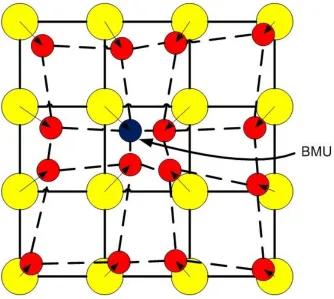
Figure 3. 2 Analogy of the SOM concept [45, 46]. ... 24
Figure 3. 3 Update stage of SOM algorithm. ... 25
Chapter 4 Figure 4. 1 SOM operational flow - OpenCL FPGA. ... 31
Chapter 5 Figure 5. 1 Visual representation of sample dataset for computation... 38
Figure 5. 2 Block Diagram of Inferred RTL Circuit for SOM FPGA implementation. ... 39
Figure 5. 3 State-Machine view of SOM FPGA design. ... 39
xi
xii
Figure 5. 17 Comparison of execution time for SOM implementation between CPU and FPGA. ... 57 Figure 5. 18 Comparison of throughput for SOM implementation between CPU and FPGA. ... 57 Figure 5. 19 Speedup comparison between FPGA and CPU... 58 Figure 5. 20 Comparison of execution time for SOM implementation between GPU and FPGA. ... 59 Figure 5. 21 Comparison of throughput for SOM implementation between GPU and FPGA. ... 59 Figure 5. 22 Speedup comparison between FPGA and GPU ... 60 Figure 5. 23 Comparison of throughput for SOM implementation between Stratix V and Arria 10 FPGAs for different map sizes. ... 61 Figure 5. 24 Comparison of throughput for SOM implementation between Stratix V and Arria 10 FPGAs for different dimensions. ... 61 Figure 5. 25 Stratix V FPGA resource utilization for different map sizes. ... 64 Figure 5. 26 Arria 10 FPGA resource utilization for different map sizes. ... 64 Figure 5. 27 Stratix V FPGA clock frequency kernel (fmax) for different input sizes.65
Figure 5. 28 Arria 10 FPGA clock frequency kernel (fmax) for different input sizes.65
xiii
xiv
List of Abbreviations
ML Machine Learning
AI Artificial Intelligence
SOM Self-Organizing Map
ANN Artificial Neural Network
FPGA Field-Programmable Gate Array
HDL Hardware Description Language
SDK Software Development Kit
IFSO Intel FPGA SDK for OpenCL
OpenCL Open Computing Language
HLS High-Level Synthesis
HLL High-Level Language
CPU Central Processing Unit
GPU Graphics Processing Unit
HPC High Performance Computing
IT Information Technology
VHDL VHSIC Hardware Description Language
VHSIC Very High Speed Integrated Circuit
AOC Altera Offline Compiler
CUDA Compute Unit Device Architecture
xv
BMU Best Matching Unit
API Application Programming Interface
DPLL Digital Phase-Locked Loop
TSP Travelling Salesman Problem
IP Intellectual Property
PCIe Peripheral Component Interconnect Express
DMA Direct Memory Access
CAD Computer-Aided Design
DDR Double Data Rate
SDRAM Synchronous Direct Random Access Memory
ALM Arithmetic Logic Module
I/O Input/Output
DSP Digital Signal Processing
RTL Register Transfer Level
PLL Phase-Lock Loop
LB Logic Blocks
LE Logic Elements
FLOPS Floating Point Operations Per Second
LU Logic Utilization
ALUTs Adaptive Look-Up Tables
xvi
PE Processing Element
SIMD Single Instruction Multiple Data
SPMD Single Program Multiple Data
SISD Single Instruction Stream Single Data Stream
MISD Multiple Instruction Single Data
1
Chapter 1. Introduction
1.1 Motivation
The demand for ML has been increasing at an exponential rate due to its ability to provide actionable insights and achieve key goals in industry and business organizations. ML algorithms have been widely used in applications involving analysis of large amounts of data in order to find patterns, make predictions, etc. One of the most important characteristics of ML is its ability to solve complex computationally intensive problems efficiently. Self-Organizing Map (SOM) [1] is an unsupervised ML algorithm and is a form of ANN. SOM, being computationally intensive, consumes a lot of hardware resources, power and takes longer execution time as the dataset size increases. The inherently parallel nature of the algorithm makes it suitable for implementation in many core and multi-core architectures. A lot of research has been done on porting ML algorithms to parallel and heterogeneous platforms [2 - 5].
2
FPGAs are programmable logic devices that provides greater flexibility and high throughput. The designs implemented in FPGA are mainly done using HDLs such as Verilog and VHSIC Hardware Description Language (VHDL) requiring extensive hardware knowledge thereby increasing the development time and cost. To exploit the potential of FPGAs fully and to make it accessible to all software developers, HLS tools such as IFSO [8] provides the opportunity to program FPGAs using HLL such as OpenCL, C and C++ without requiring extensive hardware knowledge thus efficiently accelerating computationally intensive tasks. Optimized Verilog modules are automatically synthesized into FPGA hardware binaries to be able to run on FPGA boards from HLL using the Altera Offline Compiler (AOC). Since IFSO makes the use of FPGAs accessible to all developers without requiring extensive hardware knowledge, the development and deployment of a design and the time to market for HLS-based design is significantly lower compared to RTL-based design [2, 3, and 9]. FPGAs provide the benefit of low power consumption and the fact that pipelines can be efficiently customized in FPGAs, fine-tuned for the algorithm to be accelerated, makes FPGAs a better choice compared to CPUs and GPUs.
3
kernel code. The host is responsible for initializing the device for OpenCL computation, managing hardware resources such as assigning device buffers, memory synchronization and calling the execution of kernels, whereas the computational part of the algorithm for acceleration is coded on to the kernels. The host source code is written using C/C++ and executed on the host CPU using the standard C/C++ compiler whereas the kernel code is written in OpenCL and compiled using AOC into FPGA image to be executed on the desired FPGA hardware. As the kernels take a long time to compile, they are compiled offline using AOC before the execution starts [12 - 14].
However, there are some drawbacks to using HLS. In some cases hardware synthesis using HLS may not be as efficient as hardware designed by expert skilled engineers using HDL, due to the automatic generation of the design by the software. Furthermore, due to the architectural limitations of FPGAs not all algorithms will be efficient for acceleration using HLS.
1.2 Thesis Objective
4
1. The fundamentals of parallel programming and IFSO were studied.
2. The SOM algorithm was implemented on CPU and GPU (using CUDA) for comparison of performance and power consumption with FPGAs.
3. Improvements were made in the baseline FPGA implementation by restructuring the operational flow of the SOM implementation, optimized for acceleration using IFSO.
4. An analysis of speedup in terms of execution time and throughput, resource utilization and power consumption was conducted between:
a. FPGAs and CPU b. FPGAs and GPU
c. Stratix V and Arria 10 FPGAs.
5 1.3 Thesis Outline
The remainder of this research is organized as follows:
In Chapter 2, we discuss High-Performance Computing (HPC), FPGAs, HLS, OpenCL and IFSO.
In Chapter 3, we discuss the SOM algorithm in brief and provide a review of the previously published SOM implementations targeting FPGA, CPU and GPU - based HPC platforms.
In Chapter 4, we present an optimized operational flow designed for SOM OpenCL FPGA implementation.
In Chapter 5, we present the synthesis results obtained for SOM implementation on FPGAs and compare the results with our own CPU and GPU implementations and previously published SOM research targeting CPUs and GPUs.
6
Chapter 2. Computing Platforms and CAD Tools
This chapter gives a brief introduction to High Performance computing (HPC) and HPC platforms, FPGAs, HLS, OpenCL and IFSO.
2.1 High-Performance Computing (HPC)
7
Figure 2. 1 High Performance Computing overview and applications [17]
An HPC architecture consists of compute servers called nodes networked to form clusters and a data storage facility as shown in Fig. 2.2. Each of the nodes in a cluster can communicate with each other and the data storage facility to provide maximum performance in solving computationally intensive problems. The nodes operate on the complex task in a parallel manner thereby boosting speed of execution. Hence, organizations have focused on using parallel computing and multi core designs in their Information Technology (IT) infrastructures to obtain efficient, reliable, fast and accurate solutions.
Figure 2. 2 High Performance Computing Architecture [15].
8
might run more efficiently on CPU compared to other platforms. Heterogeneous Computing (HC) overcomes this constraint by allowing the use of multiple types of processors, coprocessors and cores to execute particular tasks [18, 19]. For example, the sequential part of the task can be computed on CPU whereas the parallel part of the task can be assigned to be executed on a GPU or FPGA.
Parallel computing is the simultaneous execution of a complex task, which has been broken down into several smaller tasks and assigned to each compute unit for execution at the same time [20]. Parallel computing or parallelism can be divided into:
Bit-Level Parallelism: Parallelism is achieved by increasing the processor word
size [21]. For example adding two 16-bit numbers using 16-bit processor instead of an 8-bit processor.
Instruction-Level Parallelism: Parallelism is achieved by instruction pipelining,
superscalar execution, out-of-order execution, register renaming, speculative execution and branch prediction techniques [22]. In Instruction-Level Parallelism, several instructions are executed per clock cycle by the processor.
Data-Level Parallelism: Parallelism is achieved by distributing the data across
several compute units (i.e. nodes) for parallel execution of data. In other words is the simultaneous execution of the same task by each processor in a multi-processor environment on different distributed data [23].
Task-Level Parallelism: Parallelism is similar in this case to data-level parallelism
9
[24]. Different tasks are assigned to each processor using the same data for execution.
Traditionally, multi-core CPUs were used as HPC clusters. CPU employs instruction-level parallelism and due to its high clock frequency, it is optimized for latency. In order to minimize memory operations, CPUs employ complicated caching schemes and have large amount of on-chip caches. GPUs on the other hand are optimized for throughput and is now being used in HPC clusters. GPUs also makes use of caches similar to CPU to minimize memory access but has far fewer caches compared to CPUs. GPU uses its high memory bandwidth and parallel execution capability to maximize throughput. The use of programming APIs such as OpenCL and CUDA have made it possible for developers to easily program GPUs for computation. However, one of the drawbacks of using GPUs is its high power consumption. FPGAs have reconfigurable resources and can be reprogrammed achieving high throughput at low power consumption, which makes FPGAs a good candidate for HPC [25].
2.3 Field-Programmable Gate Array (FPGA)
10
Figure 2. 3 FPGA Architecture [28]
11 (a)
(b)
Figure 2. 4 (a) Stratix V [29] and (b) Arria 10 [30] FPGA Layout.
12
These vendors also provides the option for developers to design their own accelerator by changing the reference board design [33]. The accelerator cards used in these research are Nallatech 385 (Stratix V GX A7) [34] and Nallatech 385A (Arria 10 GX 10AX115) [35]. The boards include 8GB of DDR3 SDRAM memory, with x8 Gen 3 interface. The Stratix V A7 FPGA (5SGXMA7H2F35C2) is a 28nm technology consisting of 622K Logic Elements, 234,720 ALMs, 939K Registers 664 I/Os, 2560 M20K memory blocks and 256 DSP blocks. The Arria 10 FPGA (10AX115N3F40E2SG) is a 20nm technology consisting of 1150K Logic Elements, 427,200 ALMs, 1708800 Registers, 826 I/Os, 2713 M20K memory blocks and 1518 DSP blocks.
2.4 High-Level Synthesis (HLS)
FPGAs when programmed and configured properly according to the task can achieve significant increase in performance. In-order to program FPGAs, traditionally HDL such as Verilog and VHDL are used to generate hardware design at Register Transfer Level (RTL) or gate-level. However, programming the FPGA using HDL requires developers to have extensive hardware knowledge which increases the development time and cost. As HDL requires skilled developers for programming FPGAs, most of the organizations use CPUs and GPUs as they can be programmed easily instead of FPGAs.
13
directly into optimized HDL for implementation in FPGAs. In [37], a detailed analysis of recent HLS tools has been provided. Table 2.1 gives an overview of some of the currently available HLS tools. For our research, we will be using IFSO.
Table 2. 1 Overview of currently available HLS CAD Tool [37]
Owner Compiler License Input Output
Intel
Intel FPGA SDK for OpenCL
Commercial C/C++ and
OpenCL Verilog
Xilinx VivadoHLS Commercial C/C++
SystemC
VHDL/Verilog SystemC University of
Toronto LegUp Academic C Verilog
Cadence CtoS Commercial SystemC
TLM/C++ Verilog SystemC Mentor Graphics DK Design
Suite Commercial Handel-C
VHDL Verilog
Synopsys Synphony C Commercial C/C++
SystemC VHDL/Verilog SystemC Delft University of Technology
DWARV Academic C Subset VHDL
2.5 Open Computing Language (OpenCL)
14
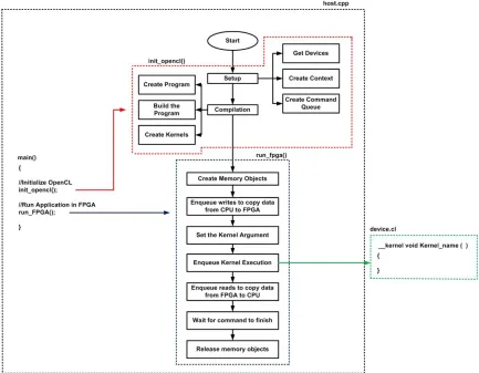
intensive tasks to be computed on one or more OpenCL-compliant devices are called kernels. The kernels are sent to the device(s) from the host. OpenCL uses a hierarchy of model [40] –
Platform Model
Memory Model
Execution Model
Programming Model
The platform model represents the host connected to the OpenCL devices as shown in Fig 2.5. The OpenCL devices are composed of Compute Units (CUs), which are composed of Processing Elements (PEs). Computation in OpenCL devices are done on the PEs.
Figure 2. 5 OpenCL Platform Model [40]
Fig 2.6 shows the memory model for OpenCL. The memory model specifies four memory regions that can be accessed:
Global Memory: The global memory can be accessed by host through
15
capabilities to all work-items in all work groups. It is the memory with largest capacity and has longer access latency and is sensitive to data access patterns.
Local Memory: A memory region that is specific to all the work-items
within a particular work-group. Local memory has lower latency compared to global memory.
Constant Memory: It is a special type of global memory, which remains
constant during kernel execution. Only the host can read/write into the constant memory, the kernels can only read data from the constant memory.
Private Memory: It is a memory region that is assigned for a particular
work-item.
16
The execution model consists of the kernel program and the host program. The execution is managed by the host by defining the context and the command queue. The context contains the following information: devices, kernels, memory objects and program objects. The programming model of OpenCL supports task as well as data based parallelism.
2.6 Intel FPGA SDK for OpenCL (IFSO)
IFSO is a HLS tool that enables developers to execute parallel computing programs easily and efficiently. It synthesizes the code written in OpenCL into optimized RTL Verilog code. The Verilog code can then be converted into FPGA hardware image by the Intel Quartus design software integrated with the IFSO tool. CPUs and GPUs use Single Instruction Multiple Data (SIMD) and/or Single Program Multiple Data (SPMD) model. IFSO allows FPGAs to support SIMD, Single Instruction Stream Single Data Stream (SISD), Multiple Instruction Single Data (MISD) and Multiple Instruction Multiple Data (MIMD) individually or in combination for computation. IFSO supports all features of OpenCL 1.0 and some features of OpenCL 1.2 and OpenCL 2.0 enabling the tool to accelerate algorithms efficiently.
17
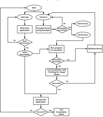
hours. Hence, the kernel source code is first compiled using the AOC. In order to check the functionality of the kernel code, it is first compiled using an emulator integrated with the IFSO tool using the command,
aoc -march=emulator --board <board_identifier> -g device/kernel.cl -o bin/kernel.aocx -v --report
Successful emulation of the kernel indicates that the kernel.cl program has no syntax, functionality, logic and stall problems. The host code is then compiled into an executable file using the standard C/C++ compiler using the command,
make –f Makefile
18
The functionality of the program is then checked using the executable file and emulated kernel files. After successful emulation, a full compilation of the application with profiling for optimization is done in AOC using the command,
aoc --board <board_identifier> --<optimization_flags> -g device/kernel.cl -o
bin/kernel.aocx -v –report
19
Figure 2. 8 Intel FPGA SDK for OpenCL (IFSO) Programming model.
2.6 Optimization Techniques - IFSO
The IFSO supports various optimization techniques for the acceleration/implementation of the algorithms directly onto the FPGA boards [13, 14].
Data Parallelism: In data parallelism, work-items in a work-group are accessed by
kernels using the SPMD/SIMD model. Each work-item executes the same operation on different data. In data parallelism, the highest throughput is achieved by the loops having no dependencies.
Task Parallelism: Task Parallelism is achieved by running the kernels using
20
AOC is achieved using multiple asynchronous command queues. Task parallelism requires the inclusion of explicit synchronization point. In task parallelism, the highest throughput is obtained when the application to be implemented on the FPGA is divided into multiple kernels.
Vectorising Work-items: Vectorising allows SIMD mode execution of read/write
as well as arithmetic/logic operations. It reduces memory access as the compiler creates kernel data path based on the number of vectors and increases memory read/write efficiency.
Loop Unrolling: Unrolling loops fully or partially by including #pragma unroll N,
where N denotes the unroll factor, before loop starts, increases the throughput of the kernel. However, increased performance comes at a cost of increased hardware resource usage as the resource usage changes based on the unrolling factor.
Compute Units (CUs): Multiple kernel compute units creates multiple copies of
the same kernel hardware for implementation simultaneously. It increases the data processing efficiency of the kernel but can cause bottlenecks in communication as the CUs share the same global memory.
Aligning Memory: Aligning Memory allows Direct Memory Access (DMA)
transfer of data to and from the FPGA increasing the data transfer efficiency. Memory alignment of host side buffers has to be at least 64-bytes aligned.
Caching Local Memory: Local memory has high bandwidth and low latency
21
memory before computation starts provides the work-items easy access to the data thereby increasing throughput.
Memory Coalescing: Memory coalescing is especially important when
reading/writing data from global memory repeatedly causing performance degradation. Memory coalescing reduces the number of memory access thereby improving memory efficiency.
Channels: Channels are First-In-First-Out (FIFO) based bus integrated in OpenCL
and supported by Intel that allows efficient data transfer between the kernels in FPGA compared to the GPU, where data transfer between kernels is achieved only through global memory. FIFOs store data in on-chip memory and has high bandwidth. Channels allow the consumer kernel to launch as soon as the producer kernel has data available for transfer. However, vectorization of work-items and creation of CUs is not possible using channels.
22
Chapter 3. Self-Organizing Map Algorithm (SOM)
3.1 Overview
In this research, we focused on the implementation and acceleration of the SOM algorithm. This chapter will first give an overview of the SOM algorithm and then will discuss some of the previous published research related to the implementation and acceleration of the SOM algorithm using HPC platforms.
3.2 Self-Organizing Map (SOM)
23
Figure 3. 1 SOM architecture.
24
Figure 3. 2 Analogy of the SOM concept [45, 46].
25
Figure 3. 3 Update stage of SOM algorithm.
Table 3. 1 Pseudo-code of SOM algorithm
ALGORITHM 1. Self-Organizing Map Algorithm
Input: Map Size (M), Dimension (D), Input Size, Initial Cluster, Dataset
Output: Resultant Cluster from dataset
for all count ϵ 0 to Max_Iteration do //Get input vector
for all i ϵ 0 to D
//Compute Euclidean distance dj between the input
//vector and each output node j
21
N
j i ij
i
d x t w t
//where,
//i and j are input and output nodes
//wij represents the weight of the connected nodes
//t represents the time end for
26
dist_index
//That node becomes the Best Matching Unit (BMU) or the //winner neuron
BMU ← dist_index
for all i ϵ 0 to M*M*D do
//Update the weight of the nodes in the map wijt 1 wij t t
x ti 1 wij t
//where,
// is the neighborhood reduction coefficient which
//decreases over time. end for
Reduce neighborhood size Reduce learning rate end for
The computation of Euclidean distance, finding the winning neuron/BMU and the update of weights of the neurons in the kohonen layer repeats several times until convergence is reached and thus accounts for most of the execution time. Euclidean distance step and the update step involves going through all the coordinates of the input vector and is the most computationally intensive part of the algorithm. The computational complexity of conventional SOM depends on the input vector size, N and the number of document presentation cycles (i.e. Euclidean distance computation stage), C and is given as (O NC) [47].
27 3.3 Related Works
Extensive research has been done on the acceleration of SOM algorithm on CPU, GPU and FPGA.
In [54], a novel implementation of SOM was conducted on GPU using two different Application Programming Interfaces (APIs), OpenCL and CUDA. Two different environments were used for evaluation, a Zotac GeGorce GT 220 on AMD Athlon 64 X2 Dual Core processor 5400+ and the Sharcnet cluster Angel consisting of 11 Nvidia Tesla S1070 GPU servers (each server consisting of 4 GPUs). Speedup achieved was in the range of 3 to 32 for various map and training data size. Experimental evaluation also showed that CUDA implementation outperformed OpenCL implementation.
In [55], a massively parallel version of SOM was implemented on Intel core 2 Duo 2.66GHz platform equipped with Nvidia GeForce 9600GT achieving speedup of 44x compared to CPU. The implementation was divided into three device kernel code calls to achieve parallelism.
28
In [57] a multi-pass method was used to find the location of the winner neuron and the update stage is then performed in reference to that position. Its dependence on low level textures enables efficient use of pipelines in solving large datasets. The SOM implementation was conducted on Intel Pentium 4, 2.4 GHz platform equipped with ATI 9550 and Nvidia 5700 GPU. In this implementation, GPU outperformed CPU especially for large datasets. The unique feature of this research was the accuracy resulting from the use of floating-point computation and the use of commodity graphics hardware which is easily available and widely used.
In [7], a parallel implementation of SOM was proposed using OpenCL on GPU. In this implementation, Manhattan distance was proposed compared to Euclidean distance to find the BMU. The concept of this research and the visual representation technique will be used while conducting our research. Comparison of performance of the parallel SOM implementation was conducted on AMD Operton 6366HE 1.8GHz processor, Intel core i7-2600 3.4GHz processor and Nvidia GeForce GTX 590 GPU. The output of the implementations were validated against a widely used package, SOM_PAK. OpenCL GPU implementation achieved speedup of upto 10x compared to SOM_PAK implementation on CPU.
29
In [59] the SOM algorithm was applied to the Travelling Salesman Problem (TSP) for a robotic mobile agent application employing embedded parallel pipeline solution (i.e. parallel pipeline architecture and parallel computation of the output and the weight update). Real-time testing of the system was achieved by generating an IP core and integrating it to a Microblaze processor bus system. The implementation was done on VHDL and the solution on FPGA showed better performance compared to CPU.
30
Chapter 4. Optimized OpenCL Model for FPGA Implementation
4.1 Overview
The aim of this chapter is to discuss the operation flow that we implemented in our research towards achieving high throughput and reduced power consumption using the IFSO HLS tool.
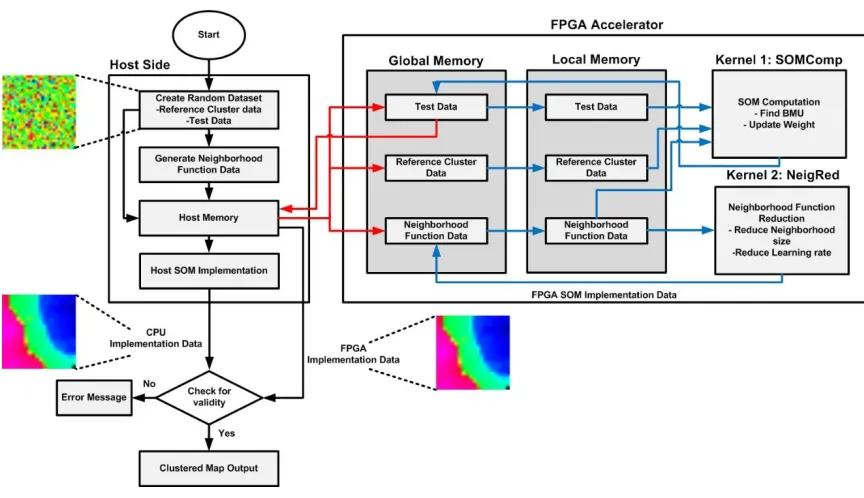
4.2 SOM Model for FPGA OpenCL Implementation
31
completed if the host side implementation matches with that of the FPGA implementation.
Figure 4. 1 SOM operational flow - OpenCL FPGA.
32
We decided to divide our implementation into two device kernel code calls. The first kernel (i.e. SOMComp kernel) Algorithm 2, takes care of the finding the winner neuron/BMU and the updating of weights of the BMU and surrounding neurons according to the neighborhood size and the learning rate. In contrast to the Euclidean distance equation (1) used in the conventional SOM we decided to use Manhattan Distance, equation (2) as suggested in [2 and 7] to find the BMU. Manhattan distance calculates the sum of the absolute value of the difference between two points thus requiring less resources compared to Euclidean distance computation by eliminating complex square and square root operations.
21
N
j i ij
i
d x t w t
(1)
1
N
j i ij
i
d x t w t
(2)2 2 ( ) 2 2 S G e NR G (3)
33
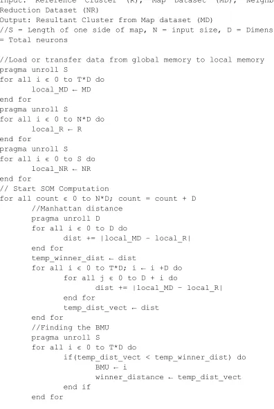
Table 4. 1 Pseudo-code of kernel 1 for SOM algorithm
ALGORITHM 2. Kernel 1 – SOMComp
Input: Reference Cluster (R), Map Dataset (MD), Neighborhood Reduction Dataset (NR)
Output: Resultant Cluster from Map dataset (MD)
//S = Length of one side of map, N = input size, D = Dimension, T = Total neurons
//Load or transfer data from global memory to local memory pragma unroll S
for all i ϵ 0 to T*D do local_MD ← MD end for
pragma unroll S
for all i ϵ 0 to N*D do local_R ← R end for
pragma unroll S
for all i ϵ 0 to S do local_NR ← NR end for
// Start SOM Computation
for all count ϵ 0 to N*D; count = count + D //Manhattan distance
pragma unroll D for all i ϵ 0 to D do
dist += |local_MD – local_R| end for
temp_winner_dist ← dist
for all i ϵ 0 to T*D; i ← i +D do for all j ϵ 0 to D + i do
dist += |local_MD – local_R| end for
temp_dist_vect ← dist end for
//Finding the BMU pragma unroll S
for all i ϵ 0 to T*D do
if(temp_dist_vect < temp_winner_dist) do BMU ← i
winner_distance ← temp_dist_vect end if
34
//Update weights of BMU and neighboring neurons for all i ϵ 0 to T*D do
local_MD ← local_MD – ((local_MD – local_R) * local_NR)
end for end for
//Load or transfer data from local memory to global memory for all i ϵ 0 to T*D do
MD ← local_MD end for
The second kernel (i.e. NeigRed kernel) Algorithm 3, takes care of reducing the neighborhood size and the learning rate for next iterations of the SOM implementation by simply shifting all the element in the NR vector to the element before it and filling the end of the vector with zero.
Table 4. 2 Pseudo-code of kernel 2 for SOM algorithm
Algorithm 3. Kernel 2 – NeigRed
Input: Neighborhood Reduction Dataset (NR) Output: Neighborhood Reduction Dataset (NR) //S = Length of one side of map
//Load or transfer data from global memory to local memory pragma unroll S
for all i ϵ 0 to S local_NR ← NR end for
Pragma unroll S for all i ϵ 1 to S
temp ← local_NR[i] local_NR[i - 1] ← temp end for
35
//Load or transfer data from local memory to global memory pragma unroll S
for all i ϵ 0 to S NR ← local_NR end for
36
Chapter 5. Experimental Results and Analysis
5.1 Overview
The aim of this chapter is to evaluate the acceleration results obtained for the proposed SOM algorithm on IFSO. We start by outlining the experimental setup for the implementation, dataset used, synthesis results and finally we compare the performance of our SOM-FPGA implementation in terms of speedup (execution time and throughput) and power consumption against other SOM implementations using CPU and GPU presented in previously published research.
5.2 Experimental Setup
37
GB/s of memory bandwidth and 384 Nvidia CUDA® cores and implementation result from [7] using Nvidia GeForce GTX 590 (40nm process) GPU.
5.3 Dataset Generation
For our research, we conducted multiple tests with different map sizes (8x8 - 64 neurons, 12x12 – 144 neurons, 16x16 – 256 neurons, 20x20 – 400 neurons and 24x24 – 576 neurons respectively), input sizes (1024, 2048, 3072, 4096 and 5120 respectively) and dimensions (3, 4, 5 and 6 respectively). We generated random floating-point data from 0 to 10000(unsigned) and used it as dataset for computations. We selected different map sizes, input sizes and dimensions in order to evaluate its effect on FPGA performance compared to CPU and GPU. The dataset was generated in order to have similar parameter setting as that proposed in previous research, which will allow us to compare our FPGA implementation with the results published in [7]. Fig 5.1 shows an example of the dataset visualized by pixels using technique mentioned in [7 and 64] where each pixel in the map represents a neuron.
38
Figure 5. 1 Visual representation of sample dataset for computation.
5.4 Synthesis Results
39
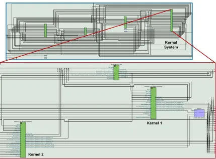
Figure 5. 2 Block Diagram of Inferred RTL Circuit for SOM FPGA implementation.
Figure 5. 3 State-Machine view of SOM FPGA design.
40
of the FPGA design. Chip planner provides a visual display of the device resources, illustrating the arrangement of the resource atoms (i.e. Arithmetic Logic Modules (ALMs), Phase-Lock Loops (PLLs), DSP blocks, Memory blocks and I/O elements) in the device architecture. Fig. 5.4 shows the chip view of our SOM design on both Stratix V and Arria 10 FPGAs. The blocks labelled as board_region, ddr_region, board_inst and
freezer_wrapper_inst denotes logic lock regions. The light green (i.e. vertical lines) represent the memory cells and the blue cells represents the Logic Blocks (LBs). Each LB consists of 16 individual Logic Elements (LEs). LBs utilized by our SOM design are indicated by a deeper blue shade.
41 (b)
Figure 5. 4 Chip view of SOM design (a) Stratix V and (b) Arria 10.
42 (a)
(b)
Figure 5. 5 Chip view indicating routing congestion of SOM design (a) Stratix V and (b)
43
Fig. 5.6 represents the power map of the SOM FPGA design indicating the High-Speed/Low-Power Tiles consisting of ALMs for both Stratix V and Arria 10 FPGAs. The tiles are differentiated by contrasting colors, where the yellow color represents High-Speed Tiles and deep blue color represents Low-Power Tiles.
44 (b)
Figure 5. 6 Power Map of SOM design (a) Stratix V and (b) Arria 10.
5.5 Performance Analysis
The datasets were tested by launching the host program with different map sizes, input sizes and dimensions separately for both FPGA and GPU implementations. Automated test scripts were used for running the program and for generating and comparing experimental results in this research. The performance for different tests is measured by execution time in seconds (s), throughput in Floating Point Operations Per Second (FLOPS) and power in Watts (W).
5.5.1 Implementation in CPU
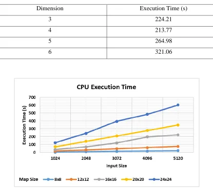
45
execution time for the SOM-CPU algorithm implementation for a map size of 16x16 with 5120 inputs and varying dimensions.
Table 5. 1 SOM-CPU execution time for different map and input sizes
Input size Execution time (s) for different Map Sizes
8x8 12x12 16x16 20x20 24x24
1024 5.02 16.32 35.50 71.43 122.92
2048 9.24 31.39 69.47 140.35 242.64
3072 13.62 46.09 120.60 209.66 396.08
4096 17.81 60.96 196.44 278.91 485.25
5120 22.02 76.02 224.21 349.11 603.87
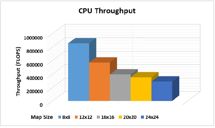
Table 5. 2 SOM-CPU throughput for different map and input sizes
Input size Throughput (FLOPS) for different Map Sizes
8x8 12x12 16x16 20x20 24x24
1024 783298.80 542283.79 443097.73 344061.94 287908.62 2048 851209.01 563669.72 452792.12 350212.68 291698.46 3072 866368.98 575825.05 391249.97 351655.06 268046.99 4096 883333.71 580506.86 320273.67 352457.78 291723.10 5120 893063.82 581910.02 350753.75 351983.78 293021.04 Average
46
Table 5. 3 SOM-CPU Implementation for different dimensions
Dimension Execution Time (s)
3 224.21
4 213.77
5 264.98
6 321.06
Figure 5. 7 Raw execution time for SOM on AMD Athlon II CPU for different map and
47
Figure 5. 8 Raw throughput for SOM on AMD Athlon II CPU for different map and input
sizes.
The execution result of the SOM algorithm in CPU are shown in Fig 5.7 in terms of execution time (s) and Fig. 5.8 in terms of throughput (FLOPS). It can be observed that as the map size and input size increases, the execution time increases and the throughput decreases.
5.5.2 Implementation in GPU
48
Table 5. 4 SOM-GPU execution time for different map and input sizes
Input size Execution time (s) for different Map Sizes
8x8 12x12 16x16 20x20 24x24
1024 8.75 31.99 69.25 149.04 257.73
2048 17.49 63.96 138.49 298.18 515.55
3072 26.23 95.96 207.73 447.31 773.31
4096 34.97 127.96 276.97 596.34 1031.07
5120 43.73 159.98 346.32 745.43 1288.93
Table 5. 5 SOM-GPU throughput for different map and input sizes
Input size Throughput (FLOPS) for different Map Sizes
8x8 12x12 16x16 20x20 24x24
1024 449543.84 276601.01 227131.66 164893.12 137311.54 2048 449723.80 276652.91 227149.70 164839.48 137289.43 3072 449766.66 276598.13 227151.34 164823.45 137290.76 4096 449788.10 276557.78 227149.70 164845.56 137292.10 5120 449646.66 276521.48 227081.81 164844.67 137281.92 Average
Throughput 449693.81 276586.26 227132.8392 164849.25 137293.15
Table 5. 6 SOM-GPU implementation for different dimensions
Dimension Execution Time (s)
3 346.32
4 322.78
5 435.86
49
The execution result of the SOM algorithm in GPU are shown in Fig 5.9 in terms of execution time (s) and Fig. 5.10 in terms of throughput (FLOPS). It can be observed that as the map size and input size increases, the execution time increases and the throughput decreases.
Figure 5. 9 Raw execution time for SOM on Nvidia Quadro K620 GPU for different map
and input sizes.
Figure 5. 10 Raw throughput for SOM on Nvidia Quadro K620 GPU for different map
50 5.5.3 Implementation in FPGA
The SOM algorithm was implemented in Intel FPGA SDK for OpenCL on Stratix V and Arria 10 FPGA accelerator boards. Table 5.7 and Table 5.8, shows the execution time for the SOM-FPGA algorithm implementation on Stratix V and Arria 10 FPGA for different map and input sizes. Table 5.9 and Table 5.10, shows the throughput for the SOM-FPGA algorithm implementation on Stratix V and Arria 10 FPGA for different map and input sizes. Table 5.11 and Table 5.12, shows execution time for the SOM-FPGA algorithm implementation on Stratix V and Arria 10 SOM-FPGA for a map size of 16x16 with 5120 inputs and varying dimensions. The execution result for the SOM algorithm in FPGA are shown in Fig 5.11 and Fig. 5.12 in terms of execution time (s) and Fig. 5.13 and Fig. 5.14 in terms of throughput (FLOPS). It can be observed that as the map size and input size increases, the execution time increases and the throughput decreases.
Table 5. 7 SOM-FPGA execution time on Stratix V FPGA for different map and input
sizes
Input size Execution time (s) for different Map Sizes
8x8 12x12 16x16 20x20 24x24
1024 3.74 15.38 29.18 55.29 97.56
2048 7.44 33.62 58.80 110.25 210.04
3072 12.35 40.78 98.50 188.83 330.19
4096 16.34 54.60 128.71 251.76 436.99
51
Table 5. 8 SOM-FPGA execution time on Arria 10 FPGA for different map and input
sizes
Input size Execution time (s) for different Map Sizes
8x8 12x12 16x16 20x20 24x24
1024 3.43 12.38 28.13 53.77 87.33
2048 7.55 32.58 54.07 107.10 185.25
3072 10.37 34.70 81.57 159.74 288.66
4096 14.27 46.59 107.55 214.65 384.14
5120 17.97 56.56 137.63 280.17 477.04
Table 5. 9 SOM-FPGA throughput on Stratix V FPGA for different map and input sizes
Input size Throughput (FLOPS) for different Map Sizes
8x8 12x12 16x16 20x20 24x24
1024 1050219.94 575399.50 539116.03 444479.11 362740.28 2048 1057612.24 526383.08 534990.29 445831.09 336984.89 3072 955584.16 650858.79 479060.68 390442.40 321539.92 4096 962346.13 648118.12 488813.88 390469.28 323937.85 5120 1007934.99 683954.25 493934.88 390490.20 333194.28 Average
52
Table 5. 10 SOM-FPGA throughput on Arria 10 FPGA for different map and input sizes
Input size Throughput (FLOPS) for different Map Sizes
8x8 12x12 16x16 20x20 24x24
1024 1148012.90 714396.11 559115.89 457022.57 405217.21 2048 1041028.96 543040.52 581822.31 458950.62 382067.60 3072 1137330.22 764883.45 578443.42 461558.66 367798.62 4096 1102357.37 759549.68 584962.40 457974.16 368504.48 5120 1094182.46 782075.46 571416.74 438588.87 370927.38 Average
Throughput 1104582.38 712789.04 575152.15 454818.98 378903.06
Table 5. 11 SOM-FPGA implementation on Stratix V FPGA for different dimensions
Dimension Execution Time (s)
3 159.22
4 97.03
5 170.71
6 198.52
Table 5. 12 SOM-FPGA implementation on Arria 10 FPGA for different dimensions
Dimension Execution Time (s)
3 137.63
4 75.72
5 152.03
53
Figure 5. 11 Raw execution time for SOM on Stratix V FPGA for different map and input
sizes.
Figure 5. 12 Raw execution time for SOM on Arria 10 FPGA for different map and input
54
Figure 5. 13 Raw throughput for SOM on Stratix V FPGA for different map and input
sizes.
Figure 5. 14 Raw throughput for SOM on Arria 10 FPGA for different map and input
55
5.5.4 Performance Comparison between CPU and FPGA
Fig. 5.15 and Fig. 5.16, shows the execution time and throughput (FLOPS) comparison for different map sizes and dimensions for AMD Athlon II CPU, Stratix V FPGA and Arria 10 FPGA respectively. It is observed that for all map sizes Arria 10 FPGA gives the highest throughput followed by Stratix V FPGA, AMD Athlon II CPU gives the lowest throughput in all cases compared to the FPGA devices. The implementation in Fig 5.16 by varying dimensions was done for map size of 16x16 – 256 neurons with input size of 5120 points.
Figure 5. 15 Comparison of throughput for SOM implementation on AMD Athlon II
56
Figure 5. 16 Comparison of throughput for SOM implementation on AMD Athlon II
CPU, Stratix V and Arria 10 FPGAs for different dimensions.
57
Figure 5. 17 Comparison of execution time for SOM implementation between CPU and
FPGA.
Figure 5. 18 Comparison of throughput for SOM implementation between CPU and
58
Figure 5. 19 Speedup comparison between FPGA and CPU.
5.5.5 Performance Comparison between GPU and FPGA
59
Figure 5. 20 Comparison of execution time for SOM implementation between GPU and
FPGA.
Figure 5. 21 Comparison of throughput for SOM implementation between GPU and
60
Figure 5. 22 Speedup comparison between FPGA and GPU
5.5.6 Performance Comparison between FPGAs
61
Figure 5. 23 Comparison of throughput for SOM implementation between Stratix V and
Arria 10 FPGAs for different map sizes.
Figure 5. 24 Comparison of throughput for SOM implementation between Stratix V and
62 5.6 Resource Utilization
Evaluation of resource utilized by the kernels are conducted by compiling the kernel using the AOC compiler for different data features such as map and input sizes and dimensions. The clock frequency (Kernel fmax) and hardware utilization such as
63
Table 5. 13 Stratix V FPGA resource utilization for different map sizes
Map Size Logic
Utilization ALUTs
Dedicated Logic Registers
Memory
Blocks DSP Blocks
8x8 28 17 12 26 5
12x12 30 18 13 29 7
16x16 30 17 14 27 5
20x20 31 19 14 33 7
24x24 32 19 14 32 7
Table 5. 14 Arria 10 FPGA resource utilization for different map sizes
Map Size Logic
Utilization ALUTs
Dedicated Logic Registers
Memory
Blocks DSP Blocks
8x8 39 15 24 22 6
12x12 40 16 25 24 7
16x16 40 15 25 23 6
20x20 41 16 25 29 7
64
Figure 5. 25 Stratix V FPGA resource utilization for different map sizes.
65
Figure 5. 27 Stratix V FPGA clock frequency kernel (fmax) for different input sizes.
66
Table 5. 15 Stratix V FPGA resource utilization for different dimensions
Map Size Logic
Utilization ALUTs
Dedicated Logic Registers
Memory
Blocks DSP Blocks
8x8 30 17 14 27 5
12x12 28 17 13 25 0
16x16 31 18 14 31 5
20x20 31 18 14 31 5
24x24 30 17 14 27 5
Table 5. 16 Arria 10 FPGA resource utilization for different dimensions
Map Size Logic
Utilization ALUTs
Dedicated Logic Registers
Memory
Blocks DSP Blocks
8x8 40 15 25 23 6
12x12 39 15 24 21 6
16x16 41 16 25 27 7
20x20 41 16 25 27 7
67
Figure 5. 29 Stratix V FPGA resource utilization for different dimensions.
68 5.7 Energy Efficiency
In order to calculate the power consumption by various HPC platforms implementing the SOM algorithm we used “Watts up? Pro” power meter [65], which can be used to obtain true power consumed by the device with an accuracy of 1.5%. Table 5.17 shows the power consumption for two CPUs and FPGAs and GPU during the idle mode and program execution mode. The idle power corresponds to the power of the workstations when no computational tasks are assigned to them. The idle + execution power corresponds to the power obtained during the SOM algorithm execution in the respective devices. The actual execution power of the SOM algorithm was obtained by subtracting the Idle Power from the (Idle + Execution Power).
Table 5. 17 Power Consumption of CPUs, GPU and FPGAs.
System
CPU with Stratix V Board
CPU with Arria 10 Board
CPU with Nvidia Quadro K620 Board CPU only CPU with Board CPU only CPU with Board CPU only CPU with Board
Idle Power (W) 76.80 76.80 139.60 139.60 76.80 76.80 Idle + Execution
Power (W) 107.00 77.65 175.50 141.87 107.00 112.95 Actual Execution
69
Figure 5. 31 SOM algorithm execution power for CPU, GPU and FPGAs.
70
Figure 5. 32 Comparison of efficiency (i.e. in terms of power) obtained using FPGA compared to CPU and GPU.
5.8 Verification
71
For the purpose of verification of our implementations, we employed a way to visually represent our resultant clustered dataset similar to the way implemented in [7 and 59]. Similar visual representations were obtained in case of CPU, GPU and FPGA for all data sets indicating the correctness our SOM implementation. Sample visual representation of the resultant clustered data obtained from CPU, GPU and FPGA is shown in Fig. 5.33.
CPU GPU FPGA
Sample 1
Sample 2
Figure 5. 33 Visual representation of SOM resultant clustered data obtained from HPC
72
Chapter 6 Conclusion
An optimized FPGA based acceleration of SOM algorithm was implemented using IFSO. HLS implementation using Stratix V and Arria 10 FPGAs of SOM was evaluated against other HPC platforms such as CPUs and GPUs. We had to efficiently restructure the operational flow of the SOM algorithm to fully take advantage of the parallel nature of the algorithm.
Our FPGA implementation using Stratix V and Arria 10 was able to achieve speedup of 16.55x and 19.15x Vs AMD Operton CPU, 1.41x and 1.63x Vs AMD Athlon II CPU and 2.53x and 2.93x Vs Intel CPU respectively. Compared to Nvidia Quadro K620 GPU, our implementation using Stratix V and Arria 10 FPGA, achieved speedup of 2.18x and 2.52x respectively. Moreover, Arria 10 FPGA achieved speedup of 1.12x compared to Stratix V FPGA. In terms of power, Stratix V and Arria 10 are 35.53x and 15.82x more power efficient compared to CPU and 42.53x and 15.93x more power efficient compared to Nvidia Quadro K620 GPU.
73
References
[1]H. Hikawa and Y. Maeda, "Improved Learning Performance of Hardware Self-Organizing Map Using a Novel Neighborhood Function," in IEEE Transactions on Neural Networks and Learning Systems, vol. 26, no. 11, pp. 2861-2873, Nov. 2015. doi: 10.1109/TNNLS.2015.2398932.
[2]Qing Y. Tang and Mohammed A. S. Khalid. 2016. Acceleration of k-Means Algorithm Using Altera SDK for OpenCL. ACM Trans. Reconfigurable Technol. Syst. 10, 1, Article 6 (September 2016), 19 pages. DOI: https://doi.org/10.1145/2964910.
[3]Momen, Mohammad Abdul. "FPGA-Based Acceleration of Expectation Maximization Algorithm using High Level Synthesis." MASc Thesis, University of Windsor, 2017. [4]Yixing Li, Zichuan Liu, Kai Xu, Hao Yu, and Fengbo Ren. 2018. A
GPU-Outperforming FPGA Accelerator Architecture for Binary Convolutional Neural Networks. J. Emerg. Technol. Comput. Syst. 14, 2, Article 18 (July 2018), 16 pages. DOI: https://doi.org/10.1145/3154839.
[5]Kaiyuan Guo, Shulin Zeng, Jincheng Yu, Yu Wang, and Huazhong Yang. 2019. [DL] A Survey of FPGA-based Neural Network Inference Accelerators. ACM Trans. Reconfigurable Technol. Syst. 12, 1, Article 2 (March 2019), 26 pages. DOI: https://doi.org/10.1145/3289185.
74
[7]Davidson, Gavin. "A parallel implementation of the self organising map using OpenCL." Level 4 Project, School of Computing Science, University of Glasgow (2015).
[8]Intel FPGA SDK for OpenCL, [Online] Available from -
https://www.intel.com/content/www/us/en/software/programmable/sdk-for-opencl/overview.html. [Accessed August 13, 2019]
[9]Luthra, Siddhant. "High level synthesis and evaluation of an automotive radar signal processing algorithm for fpgas." MASc Thesis, University of Windsor, 2017.
[10]The Khronos Group Inc., [Online] Available from - https://www.khronos.org/. [Accessed August 13, 2019].
[11]Sanders, Jason, and Edward Kandrot. CUDA by example: an introduction to general-purpose GPU programming. Addison-Wesley Professional, 2010.
[12]Altera SDK for OpenCL – Getting Started Guide. [Online] Available from -https://www.intel.com/content/dam/www/programmable/us/en/pdfs/literature/hb/open
cl-sdk/archives/ug-aocl-getting-started-16.0.pdf. [Accessed August 13, 2019].
[13]Altera SDK for OpenCL – Programming Guide.[Online] Available from - https://www.intel.com/content/dam/www/programmable/us/en/pdfs/literature/hb/open
cl-sdk/archives/aocl-programming-guide-15.1.pdf. [Accessed August 13, 2019]. [14]Altera SDK for OpenCL – Best Practices Guide. [Online] Available from
-https://www.intel.com/content/dam/www/programmable/us/en/pdfs/literature/hb/open
75
[15]What Is High-Performance Computing? [Online] Available from - https://www.netapp.com/us/info/what-is-high-performance-computing.aspx.
[Accessed August 20, 2019]
[16]Geshi, M. (2019). The Art of High Performance Computing for Computational Science, Vol. 1. Springer.
[17]About High-Performance Computing (HPC). [Online] Available from - https://www.ichec.ie/news/press-corner/about-high-performance-computing-hpc. [Accessed August 20, 2019].
[18]Shan, Amar. "Heterogeneous processing: a strategy for augmenting moore's law." Linux Journal 2006, no. 142 (2006): 7.
[19]Zahran, M. (2019). Heterogeneous Computing: Hardware and Software Perspectives. Morgan & Claypool.
[20]Gottlieb, Allan, and G. Almasi. Highly parallel computing. Redwood City, CA: Benjamin/Cummings, 1989.
[21]Bit-level parallelism. [Online] Available from - https://en.wikipedia.org/wiki/Bit-level_parallelism. [Accessed August 20, 2019].
[22]Instruction-level parallelism [Online] Available from - https://en.wikipedia.org/wiki/Instruction-level_parallelism. [Accessed August 20, 2019].
[23]Data-level parallelism. [Online] Available from -
https://en.wikipedia.org/wiki/Data_parallelism. [Accessed August 20, 2019].
[24]Task-level parallelism. [Online] Available from -
76
[25]Inta, Ra, David J. Bowman, and Susan M. Scott. "The Chimera: an off-the-shelf CPU/GPGPU/FPGA hybrid computing platform." International Journal of Reconfigurable Computing 2012 (2012): 2.
[26]Waidyasooriya, H. M., Hariyama, M., & Uchiyama, K. (2018). Design of FPGA-based computing systems with OpenCL. Springer International Publishing.
[27]Parab, J. S., Gad, R. S., & Naik, G. M. (2018). Hands-on Experience with Altera FPGA Development Boards. Springer.
[28]FPGA Architecture. [Online] Available from - https://allaboutfpga.com/fpga-architecture/.[Accessed August 20, 2019].
[29]Stratix V FPGA Features. [Online] Available from -
https://www.intel.com/content/www/us/en/products/programmable/fpga/stratix-v/features.html. [Accessed August 20, 2019].
[30]Arria 10 FPGA Features. [Online] Available from -
https://www.intel.co.uk/content/www/uk/en/products/programmable/fpga/arria-10/features.html. [Accessed August 20, 2019].
[31]Terasic [Online] Available from - https://www.terasic.com.tw/en/.[Accessed August 20, 2019].
[32]Bittware [Online] Available from - https://www.bittware.com. [Accessed August 20, 2019].
[33]Altera Corporation, “OpenCL Reference Platforms,” [Online]. [Accessed: Dec 01, 2015]
[34]Nallatech 385 –with Stratix V A7 FPGA PCIe Accelerator Card. [Online] Available
-77
https://www.intel.com/content/www/us/en/programmable/solutions/partners/partner-profile/isi-nallatech/board/385---with-stratix-v-a7-fpga-pcie-accelerator-card.html. [Accessed August 20, 2019]
[35]Nallatech 385A –with Arria 10 FPGA PCIe Accelerator Card. [Online] Available
from -
https://www.intel.com/content/www/us/en/programmable/solutions/partners/partner-profile/isi-nallatech/board/385a---pga-accelerator-card-with-arria-10-fpga.html. [Accessed August 20, 2019]
[36]Coussy, Philippe, and Adam Morawiec, eds. High-level synthesis: from algorithm to digital circuit. Springer Science & Business Media, 2008.
[37]Nane, Razvan, Vlad-Mihai Sima, Christian Pilato, Jongsok Choi, Blair Fort, Andrew Canis, Yu Ting Chen et al. "A survey and evaluation of FPGA high-level synthesis tools." IEEE Transactions on Computer-Aided Design of Integrated Circuits and Systems 35, no. 10 (2015): 1591-1604.
[38]Scarpino, M. (2011). OpenCL in action: how to accelerate graphics and computations. Manning Publications.
[39]The Khronos Group Inc. “OpenCL Overview” [online]. Available: https://www.khronos.org/opencl/. [Accessed August 20, 2019].
[40]A. Munshi, "The OpenCL specification," 2009 IEEE Hot Chips 21 Symposium (HCS), Stanford, CA, 2009, pp. 1-314.doi: 10.1109/HOTCHIPS.2009.7478342 [41]Janik, Ian, Qing Tang, and Mohammed Khalid. "An Overview of Altera SDK for

![Figure 3. 2 Analogy of the SOM concept [45, 46].](https://thumb-us.123doks.com/thumbv2/123dok_us/1342270.1167122/41.612.149.500.70.305/figure-analogy-som-concept.webp)