c
MULTITHREADED ARCHITECTURES FOR MANYCORE THROUGHPUT PROCESSORS
BY
DANIEL R. JOHNSON
DISSERTATION
Submitted in partial fulfillment of the requirements
for the degree of Doctor of Philosophy in Electrical and Computer Engineering in the Graduate College of the
University of Illinois at Urbana-Champaign, 2013
Urbana, Illinois
Doctoral Committee:
Professor Sanjay J. Patel, Chair Associate Professor Steven S. Lumetta Professor Wen-Mei W. Hwu
ABSTRACT
This dissertation describes work on the architecture of throughput-oriented accelerator processors.
First, we examine the limitations of current accelerator processors and identify an opportunity to enable high throughput while also providing a more general-purpose programming model. To address this opportunity, we present Rigel, a single-chip accelerator architecture with 1024 independent processing cores targeted at a broad class of data- and task-parallel com-putation. Enabled by the feasibility of large die sizes combined with in-creasing transistor densities, we show that such an aggressive design can be implemented in today’s process technology within acceptable area and power limits. We discuss our motivation for such a design and evaluate the perfor-mance scalability as well as power and area requirements. We also describe the Rigel memory system, including the Task Centric Memory Model soft-ware coherence protocol, the Cohesion hybrid memory model, and lazy atomic operations.
We describe the Rigel toolflow, a set of tools we have developed for eval-uating manycore accelerator architectures. The Rigel toolset includes an architectural simulator, LLVM-based compiler, parallel benchmarks, RTL models, and associated infrastructure scripts and toolflows. We have pre-pared an open-source release of portions of the resulting toolset for the use of the broader research community. Such a release will enable others to perform further work in the area of accelerator design.
We present multi-level scheduling, a technique developed for throughput-oriented graphics processing units (GPUs) designed to reduce complexity and energy consumption. Modern GPUs employ a large number of hardware threads to hide both long and short latencies. Supporting tens of thousands of hardware threads requires a complex scheduler and a large register file which is expensive to access in terms of energy and latency. With multi-level
scheduling, we divide threads into a smaller set of active threads to hide short latencies and larger set of pending threads for hiding long latencies to main memory. By reducing the concurrently active number of threads, we enable more efficient scheduler and register file structures.
Finally, we describe opportunities for employing similarhierarchical multi-threading techniques to MIMD accelerator designs such asRigel. We extend the originalRigelarchitecture with a new multithreaded microarchitecture. We propose a novel, flexible multithreading paradigm that allows the archi-tect a flexible way to scale the number of threads to match the requirements of targeted workloads. We show that this new multithreaded architecture can be implemented efficiently while providing more flexibility to the architect.
ACKNOWLEDGMENTS
Like all successful projects, the research presented in this dissertation bene-fited from many contributions, both small and large, from a variety of people. John Kelm was instrumental in the development of the Rigel project. John’s willingness to plow ahead in the face of uncertainty was key to spin-ning up our own set of tools from scratch. I’m thankful for the frequent intellectually stimulating conversations about architecture, computers, eco-nomics, all things technical, and more. I must also thank John for the beer. Matt Johnson’s hacker expertise was an invaluable asset across the project, from simulator to compiler to benchmarks.
Special thanks to all of the students and others who contributed to the RTL portion of the Rigel project: Bill Tuohy lent his expert hand in many ways to get a realistic RTL CAD flow set up, along with Jonathan Ashbrook. Voytek Truty implemented the floating-point units in the Rigel RTL and was a valuable team contributor to the RigelRTL project. Voytek’s unique sense of humor was always a bright spot for the two years we were officemates. We will always remember Trogdor in the testflow. Simon Venshtain worked on the RTL cache models, wrangled memory macros, and helped with the test and verification flow. Jeremey (Chia-jen Chang) worked on turning our RTL project into a taped out test chip! Jeremy took the RTL and toolflow I developed with Simon and Voytek and worked it into a tapeout-ready netlist for fabrication.
I would like to thank the various faculty I’ve had a chance to collaborate with and get to know through this project.
Sanjay, for instigating a large systems project and imposing no boundaries. I am grateful for having had the opportunity to work on a large systems project where nothing was taken as fixed, enabling me to dabble in architec-ture, software engineering, parallel application development, compilers, and RTL design and implementation.
Steve Lumetta, for always taking an interest in the work of students and providing positive, insightful advice, no matter the topic.
Matt Frank for helping to get theRigel project started on the right foot. Finally, Wen-Mei and Naresh for serving on my committee.
I would like to thank all of the remaining members of the Rigel team for their various contributions over time, including Stephen Kofsky, Neal Crago, Wooil Kim, and our collective class project partners who contributed to our work, especially those who acted as guinea pigs for our tools under development. Over time, many students helped in some fashion to develop, debug, and improve the various tools used in this research.
I thank my collaborators at NVIDIA Research, Mark Gebhart, David Tar-jan, and Steve Keckler, for their contributions to the GPU-related work pre-sented here. I would also like to thank NVIDIA for a generous Graduate Fellowship award during my last year of graduate school.
I thank my family for their continued support and encouragement.
Finally, I would like to thank my wife Melanie for her love and support throughput my graduate school career, and for managing to tolerate me throughout the long process that is graduate school.
TABLE OF CONTENTS
LIST OF ABBREVIATIONS . . . ix
CHAPTER 1 INTRODUCTION . . . 1
1.1 Motivation: Current Accelerator Limitations . . . 1
1.2 Rigel: A Programmable Manycore Accelerator . . . 2
1.3 Efficient, Flexible Multithreading . . . 3
CHAPTER 2 RIGEL: A 1024-CORE SINGLE CHIP ACCELER-ATOR ARCHITECTURE . . . 6
2.1 Motivation: Current Accelerator Limitations . . . 6
2.2 Rigel Accelerator Architecture Overview . . . 7
2.3 Caching and Memory Model . . . 13
2.4 ProgrammingRigel: The Rigel Task Model . . . 16
2.5 Evaluation: Area and Power . . . 18
2.6 Evaluation: Scalability . . . 19
2.7 VLSI Implementation and Test Chip . . . 19
CHAPTER 3 RIGEL MEMORY SYSTEM . . . 25
3.1 Parallel Application Characterization . . . 26
3.2 Software-managed Coherence with the Task-Centric Mem-ory Model . . . 31
3.3 Hybrid Coherence withCohesion . . . 34
3.4 Lazy Atomic Operations . . . 36
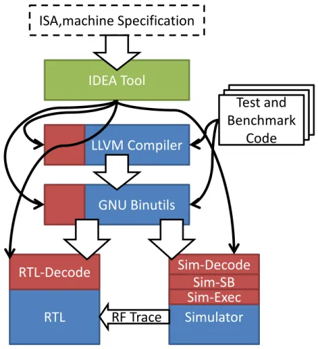
CHAPTER 4 AN EVALUATION INFRASTRUCTURE FOR MAS-SIVELY PARALLEL ACCELERATOR PROCESSORS . . . 47
4.1 Toolflow Objectives . . . 48
4.2 The Case for a Flexible, Integrated Evaluation Framework . . 48
4.3 Toolflow Components . . . 50
4.4 Tool Chain Integration: IDEA . . . 54
4.5 Timing Simulator . . . 55
4.6 Cluster . . . 56
4.7 Simulation Automation . . . 56
4.8 RTL Infrastructure . . . 57
4.10 Testing and Verification . . . 59
4.11 Summary . . . 60
CHAPTER 5 ENERGY-EFFICIENT THROUGHPUT ARCHI-TECTURES WITH MULTI-LEVEL SCHEDULING . . . 61
5.1 Introduction . . . 63 5.2 Background . . . 64 5.3 Microarchitecture . . . 70 5.4 Methodology . . . 78 5.5 Evaluation . . . 81 5.6 Conclusion . . . 92
CHAPTER 6 HIERARCHICAL MULTITHREADING . . . 94
6.1 Hierarchical Multithreaded Clusters . . . 96
6.2 A Multithreaded Microarchitecture for Rigel . . . 98
6.3 Hierarchical Multithreading . . . 104
6.4 Thread Pools: Migratory Hierarchical Multithreading . . . 110
6.5 Summary . . . 117
CHAPTER 7 RELATED WORK . . . 119
7.1 Throughput Processors . . . 119 7.2 Coherence . . . 121 7.3 Atomic Operations . . . 122 7.4 Hierarchical Multithreading . . . 122 7.5 Tools . . . 124 CHAPTER 8 CONCLUSIONS . . . 126
8.1 Rigel: Looking to the Future . . . 126
8.2 Energy Efficient Multithreading for GPUs . . . 129
8.3 Hierarchical Multithreading . . . 130
LIST OF ABBREVIATIONS
BSP Bulk Synchronous Parallel CMP Chip Multiprocessor CPU Central Processing Unit
DRAM Dynamic Random Access Memory FIFO First In, First Out
FPU Floating Point Unit
GDDR Graphics Double Data Rate GPU Graphics Processing Unit
GPGPU General-Purpose Graphics Processing Unit ILP Instruction Level Parallelism
ISA Instruction Set Architecture
MIMD Multiple Instruction Multiple Data RTL Register-Transfer Level
SIMD Single Instruction Multiple Data SIMT Single Instruction Multiple Thread SMP Symmetric Multiprocessor
SoC System on Chip
SPMD Single Program Multiple Data SRAM Static Random Access Memory VLIW Very Long Instruction Word VLSI Very Large Scale Integration
CHAPTER 1
INTRODUCTION
An insatiable appetite for performance on compute intensive data-parallel workloads in visual and scientific computing has driven the design of through-put-oriented parallel compute accelerators. For this work, we consider pro-grammableaccelerators in contrast to fixed-function or hardwired application-specific accelerator units. Such accelerators are designed to improve perfor-mance for specific classes of workloads by exploiting characteristics of the target domain and by limiting the generality of the programming model. While general-purpose processors tend to employ additional transistor re-sources to minimize latency (operationsec ), accelerators are designed to maximize throughput (operationssec ). Contemporary examples of compute accelerators in-clude graphics processing units (GPUs) [1], Cell [2], and Larrabee [3]. For a more complete discussion of throughput-oriented CMP and accelerator ar-chitectures, please see Chapter 7.
1.1
Motivation: Current Accelerator Limitations
Current accelerators generally expose restricted programming models which yield high performance for data-parallel applications with rigidly structured computation and memory access patterns, but present a more difficult tar-get for less regular parallel applications. The throughput-oriented archi-tectural design choices of accelerators often compromise the generality of the programming model. For instance, accelerators commonly achieve high throughput through the use of wide SIMD (single instruction, multiple data) processing elements, as opposed to the MIMD (multiple instruction, multi-ple data) model favored by general-purpose processors. For dense or regular data-parallel computations, SIMD hardware reduces the cost of perform-ing many computations by amortizperform-ing costs such as control and instruction
fetch across many processing elements, enabling an efficient hardware im-plementation. However, for applications that do not naturally map to the SIMD execution model, programmers must adapt their algorithms or suffer reduced efficiency, limiting the scope of applications which can achieve the hardware’s peak performance. The memory system is another area where accelerators commonly make compromises in support of hardware efficiency that limit programmability. Software-managed scratchpad memories yield denser hardware, tighter access latency guarantees, and consume less power than caches; however, they impose additional burden on either the program-mer or software tools. Multiple address spaces also increase the burden of development.
1.2
Rigel
: A Programmable Manycore Accelerator
TheRigelarchitecture was conceived in 2007 as an attempt to address some of the shortcomings of parallel computation accelerators while pushing the envelope on throughput-oriented designs. Broadly, the goals of the project are to
• Demonstrate the feasibility of a single-chip, massively parallel MIMD accelerator architecture with 1024 cores
• Achieve high computational density, or throughput (operations/secmm2 )
• Determine how to organize such a device to be programmer-friendly • Present a more general target to developers, increasing the scope of
parallel applications which can target the design
These goals drove our development of Rigel [4], a 1024-core single-chip accelerator architecture that targets a broad class of data- and task-parallel computation, especially visual computing workloads. With the Rigel de-sign, we aim to strike a balance between raw performance and ease of pro-grammability by adopting programming interface elements from general-purpose processors. Rigel is composed of 1024 independent, hierarchi-cally organized cores that use a fine-grained, dynamihierarchi-cally scheduled single-program, multiple-data (SPMD) execution model. Rigel adopts a single global address space and a fully cached memory hierarchy. Parallel work is expressed in a task-centric, bulk-synchronized manner using minimal
hard-ware support. Compared to existing accelerators, which contain domain-specific hardware, specialized memories, and restrictive programming mod-els, Rigel is more flexible and provides a more straightforward target for a broader set of applications. The Rigel architecture is described in more detail in Chapter 2.
The design of the Rigel memory system, particularly cache coherence, shaped many other aspects of the architecture. We observed that data shar-ing and communication patterns in parallel workloads can be leveraged in the design of memory systems for future manycore accelerators. Based on these insights, we developed both software and hardware mechanisms to manage coherence on parallel accelerator processors. We developed the Task-Centric Memory Model [5], a software protocol which works with hardware caches to maintain a coherent, single-address-space view of memory without hardware coherence support. We developed Lazy Atomic Operations as an extension to this model to take advantage of incoherent hardware caches for improving throughput on atomic operations. We developed Cohesion [6] as a bridge enabling effective use of both hardware and software coherence mechanisms, simplifying the integration of multiple memory models in heterogeneous or accelerator-based systems.
1.3
Efficient, Flexible Multithreading
Application characteristics and memory access behavior direct the level of threading and required latency hiding capabilities for an architecture. In throughput-oriented systems, multiple types of latencies must be hidden. A variety of short-term latencies limit performance, including pipeline hazards, functional unit latencies, cache access latency, resource contention, and lack of ILP. Traditional techniques for hiding shorter latencies, such as out-of-order processing to uncover ILP, incur a high cost in terms of area and power, undesirable for throughput-oriented designs. Additionally, long-latency op-erations including cache misses, global memory opop-erations such as atomics, and uncacheable memory accesess can introduce longer stalls.
A common solution for hiding latency and increasing throughput is hard-ware multithreading. Multithreaded systems provide hardhard-ware threads to hide both short and long latencies. These designs provide a relatively easy
path for programmers to achieve high throughput on their applications. While adding additional threads to an architecture can hide more latency and ease the burden on the programmer, hardware threads are not free. There is a large marginal cost to each hardware thread. Each hardware thread context requires additional resources, including register file storage and scheduling entries. On modern GPUs, a substantial portion of the die area is dedicated to register storage for thousands of hardware-resident threads [7]. Addition-ally, the design complexity of the pipeline, the thread scheduler, and other shared structures increases to handle the increased level of threading. Finally, over-threading causes additional contention for shared resources, which can hurt performance and throughput.
1.3.1
Power Efficient Throughput-Oriented Architectures
While aggressive throughput-oriented processors are feasible today, power is becoming an increasingly important limiter for high-performance designs [8] such as Rigel and graphics processors. Architects of future throughput processors must consider both power and performance. In Chapter 5, we describe work on energy-efficient mechanisms for managing large numbers of hardware-resident thread contexts in throughput processors.
We present multi-level scheduling, a technique developed for throughput-oriented graphics processors (GPUs) designed to reduce complexity and en-ergy consumption. Modern GPUs employ a large number of hardware threads to hide both long and short latencies. Supporting tens of thousands of hard-ware threads requires a complex scheduler and a large register file, which is expensive to access in terms of energy and latency. With multi-level schedul-ing, we divide threads into a smaller set of active threads to hide short latencies and larger set of pending threads for hiding long latencies to main memory. By reducing the concurrently active number of threads, we en-able both a lower complexity scheduler and more power-efficient register file structures.
1.3.2
Hierarchical Multithreading on Rigel
There is a wide design space between the simple, single-threaded processors originally employed by Rigel and the massively threaded processors em-ployed by modern GPUs. The level of threading desired for a given system is influenced by a variety of factors, especially for throughput-oriented accel-erator processors. Key applications and application domains have a heavy influence on the underlying architecture. For instance, graphics workloads stream through large datasets while rendering each frame and are effectively bandwidth limited, leading to large numbers of latency hiding threads in modern GPUs.
While a particular application or application domain may be matched to a specific degree of threading for a given design implementation, there is no single correct degree of multithreading. For a throughput-oriented system, the end goal is to select a design point that maximizes overall throughput.
We desire a flexible threading architecture for accelerators. We seek to take advantage of the disjoint latency classes that influence multithreaded designs to enable a more configurable multithreading paradigm. Our goal is a scal-able multithreading solution versus the typical point solutions employed by multithreaded designs today. It is desirable to consider an architecture that allows the architect to dial a knob for selecting the degree of multithreading. One knob adjusts the number of threads supported by execution pipelines, and another knob selects the number of threads available to hide memory latency.
In pursuit of this goal, we employ similar techniques as we evaluated for GPUs. We consider splitting thread contexts into two groups, L1 threads that are actively executing on a given core, and hardware-resident L2 threads that wait on memory requests and provide fast context switches.
We describe opportunities for employing similarhierarchical multithreading techniques to MIMD accelerator designs such as Rigel. We extend the originalRigelarchitecture with a new multithreaded microarchitecture. We propose a novel flexible multithreading paradigm allowing the architect a flexible way to scale the number of threads to match the requirements of targeted workloads. We show that this new multithreading paradigm can be implemented efficiently while providing more flexibility to the architect.
CHAPTER 2
RIGEL: A 1024-CORE SINGLE CHIP
ACCELERATOR ARCHITECTURE
In this chapter, we provide a description of theRigel 1024 core accelerator architecture. We describe previous work for throughput-oriented processing designs. We detail the motivation for and objectives of theRigeldesign. We describe the cores and clustered core organization, the caches and memory system, and Rigel’s task-based programming model.
This work has been most recently published in [9], and parts have been previously published in [4, 10, 5, 11, 6, 12].
2.1
Motivation: Current Accelerator Limitations
Current accelerators generally expose restricted programming models which yield high performance for data-parallel applications with rigidly structured computation and memory access patterns, but present a more difficult tar-get for less regular parallel applications. The throughput-oriented architec-tural choices of accelerators often compromise the generality of the program-ming model. For instance, accelerators commonly achieve high throughput through the use of SIMD (single instruction, multiple data) processing ele-ments as opposed to the MIMD (multiple instruction, multiple data) model. For dense or regular data-parallel computations, SIMD hardware reduces the cost of performing many computations by amortizing costs such as con-trol and instruction fetch across many processing elements. However, when applications do not naturally map to the SIMD execution model, program-mers must adapt their algorithms or suffer reduced efficiency. SIMD then limits the scope of applications which can achieve the hardware’s peak per-formance. The memory system is another area where accelerators commonly make compromises in support of hardware efficiency that limit programmabil-ity. Software-managed scratchpad memories yield denser hardware, provide
tighter access latency guarantees, and consume less power than caches; how-ever, they impose an additional burden on either the programmer or software tools. Additionally, managing the multiple address spaces often associated with accelerator memories requires copy operations and more explicit manual memory management.
2.2
Rigel
Accelerator Architecture Overview
In this section, we provide an overview of theRigelaccelerator architecture. We describe our design objectives, the major components of our design, and some possible alternative organizations.
2.2.1
Objectives
The Rigel architecture was conceived as an attempt to address some of the shortcomings of parallel computation accelerators while pushing the envelope on throughput-oriented designs.
Broadly, the goals of theRigel project were to
• Determine the feasibility of a single-chip, massively parallel MIMD gen-eralized computation accelerator
• Achieve high computation density, or throughput (operations/secmm2 )
• Determine how to organize such a device to be programmer-friendly • Present a more general target to developers, increasing the scope of
parallel applications which can target the design
• Address the limitations of existing accelerator architectures
2.2.2
Rigel
: A Programmable Manycore Accelerator
Architecture
These objectives drove our development of Rigel [4], a 1024-core single-chip accelerator architecture designed to efficiently target a wide class of regular and irregular parallel applications, including data- and task-parallel
Rigel Architecture: Full Chip View
9
Figure 2.1: Block diagram of the Rigel processor.
computation. With the Rigel design, we aim to strike a balance between raw performance and ease of programmability by adopting programming in-terface elements from general-purpose processors. A block diagram of the Rigel accelerator architecture is shown in Figure 2.1. Rigel is composed of 1024 independent, hierarchically organized cores. Simple in-order cores em-phasize throughput over latency, but a MIMD execution model is chosen for flexibility over a potentially denser SIMD model. Rigel has a fully cached, single address space memory model with no chip-wide hardware-enforced coherence in the baseline configuration. Work distribution is managed in software in a bulk-synchronous fashion. Compared to existing accelerators, which rely on domain-specific hardware, multiple special-purpose memories, and limited programming models,Rigelis more flexible and provides a more straightforward development target for a broader range of parallel applica-tions.
Tradeoffs are made in Rigel’s low-level programming interface between generality and accelerator performance. The primary elements that we iden-tify as important for supporting our objectives include the execution model, the memory model, work distribution, synchronization, and locality man-agement. The Rigel execution model omits complex ILP-oriented cores in favor of simple, area-optimized in-order cores to improve full-chip through-put. However, a more flexible MIMD model is chosen over denser SIMD hardware. A degree of multithreading is beneficial in improving throughput
Table 2.1: Comparison of Rigel to other contemporary accelerator architectures
Rigel GPU Cell Larrabee
Vectors 1× (MIMD) 32× (SIMT) 4× (SIMD) 16× (SIMD)
Memory Fully Special DMA + Fully
Cached Purpose Scratchpad Cached Address Space Single Multiple Multiple Single
Thread Count Some (1-4) Heavy None Some (4)
(per core) (10s-100s)
Core Count 1024 10s-100s 8-10 10s
Coherence HW/SW None None HW
Hybrid
Work Software Hardware Software Software
Distribution
Specialized None Significant None Some
Hardware (graphics) (texture)
and is under investigation. Unlike many accelerators,Rigelpresents a single global address space similar to general purpose CMPs. Rigel supports soft-ware work distribution in the form of task queues based on the common BSP execution model. Rigel supports global synchronization through software barriers and through atomic hardware primitives. Rigel supports a variety of memory operations to aid in locality management, including prefetches, local and global memory operations, and explicit cache management instruc-tions.
Table 2.1 compares the Rigel design point to several other notable ac-celerator processors, and Table 2.2 summarizes our design parameters. The various components of the Rigel accelerator architecture are discussed in more detail below.
2.2.3
Core
The fundamental processing element of Rigel is a dual-issue in-order core optimized for area rather than ILP. Cores support a custom 32-bit RISC-like instruction set. Each core has a standard integer pipeline, a fully pipelined single-precision floating-point unit, load-store pipeline, and 32-entry 32-bit
Table 2.2: Simulated parameters for the Rigel architecture
Cores 1024, 2-wide issue, in-order
1.5 GHz
1 single-precision floating-point unit 1 integer unit
1 memory unit
L1 I-Cache 2 kB, 2-way associative
L1 D-Cache 1 kB, 2-way associative kB
L2 (Cluster) Cache Unified, 1 per 8-core cluster 64 kB, 16-way L3 (Global) Cache Globally shared, 4 MB total, 32 8-way banks
DRAM 8 32-bit channels, GDDR5
DRAM Bandwidth 192 GB/s
general-purpose register file. A set of special purpose registers serve to pro-vide configuration information such as unique core IDs. In contrast to SIMD or SIMT machines, each pipeline has an independent front end and instruc-tion fetch unit, allowing all cores to simultaneously execute fully independent instruction streams in a MIMD fashion. Each core has a small L1 instruction cache and L1 data cache. The baseline core microarchitecture is illustrated in Figure 2.2.
2.2.4
Cluster
Cores are organized intro groups called clusters. A cluster contains a collec-tion of cores attached to a shared unified cluster cache. Figure 2.1 illustrates the cluster on the left side. The baseline Rigel configuration contains eight cores per cluster, with cores connected to the cluster cache via a shared bus. The interconnect between cores and the cluster cache is a split-phase bus, enabling simultaneous requests and responses. Clusters allow efficient communication among their cores via the shared cluster cache. Core-private caches are kept coherent across their containing cluster. Clusters also im-plement local atomics, load-linked and store-conditional. The cores, cluster cache, core-to-cluster-cache interconnect and the cluster-to-global intercon-nect logic make up a single Rigel cluster.
Exec
Fetch Decode Exec 1
(Int) Mem FPU 1 CCRead RegFile L1 I-Cache L1 D-Cache WB Mem2 Score- Board Bypass Network Exec 2
FPU 2 FPU 3 FPU 4
ClusterNet (Bus) ClusterNet (Arb) (empty) (empty) SPRF FP Accumulator RegFile
Mem FPU CCRead
Agen
2.2.5
Tile
Clusters are connected and grouped logically into a tile. The tile unit serves primarily as a unit of VLSI replication. In the 1024-core baseline configura-tion of Rigel, eight tiles of 16 clusters each are distributed across the chip. Clusters within a tile share resources on a bi-directional tree-structured inter-connect. A tree-structured interconnect is chosen as opposed to a mesh due to the intended use pattern. Communication between cores takes place via shared caches, not through explicit message passing. The interconnect serves to connect cores to memory, not to enable arbitrary core-to-core communi-cation or coherence traffic. Tiles are distributed across the chip, attached to global cachebanks via a multi-stage switch interconnect. Figure 2.1 illus-trates the tile and top-level organization on the right side.
2.2.6
Global Cache
The global cache is Rigel’s last-level shared cache and provides buffering for several high-bandwidth memory controllers. Our initial 1024-core design includes 8 GDDR memory controllers and 32 global cache banks. The global cache provides a point of coherence for memory accesses; each address may be cached in only a single location in the last-level global cache. Shared data made visible in the global cache is visible to all cores on the chip. By default, global cache misses which access DRAM result in the returned data being cached in the global cache. However, memory operations which bypass caching in the global cache are optionally available. Additionally, global atomic operations are performed at the global cache.
2.2.7
Alternate Organizations
While Rigel selects a particular set of design points, a number of promising alternatives to the baseline Rigel architecture exist.
At the cluster level, a rich design space exists in the interconnection of cores and caches as well as in core microarchitecture and degree of thread-ing. We explore only a subset of this space. The cluster-level shared cache interconnection was implemented as a split-phase shared bus in the baseline Rigeldesign as cores are single threaded and core-level caches service a large
fraction of memory traffic, reducing required bandwidth to the cluster cache. However, as more cores share the cluster cache, bandwidth demands grow. Additionally, some application classes naturally demand more bandwidth or are simply less amenable to caching. Notable variations on the cluster design include a multi-banked cache interconnected to cores by a crossbar structure as well as alternate core microarchitectures, including multithreading.
At the tile and chip level, the network-on-chip and last-level global cache organization present a number of design alternatives. While we selected our design point based on intended use cases, there are compelling arguments for alternative designs. One notable alternate design point for the tile and global cache is to include global cache banks paired with tiles, and interconnect tiles as a mesh. Each tile would be associated with fixed memory controller and global cache resources in a NUCA organization. Such a design may have desirable VLSI replication properties due to regularity.
Exhaustive exploration of all design alternatives is beyond the scope of this dissertation as well as the Rigel project.
2.3
Caching and Memory Model
All cores on the Rigel processor share a single global address space. Cores within a cluster have the same view of memory via the shared cluster cache, while cluster caches in our baseline architecture are not explicitly kept co-herent with one another. The low-level hardware operations and software model for maintaining coherence are discussed further in Chapter 3. The global cache provides a point of coherence for when software needs to syn-chronize or otherwise safely share data between separate clusters. Due to the incoherent nature of the cache hierarchy, Rigel implements two classes of memory operations: local and global.
2.3.1
Local Memory Operations
Local memory operations are the standard path to memory on theRigel ar-chitecture. Local operations are fully cached at the cluster cache, but arenot kept coherent by hardware between clusters. Local loads and stores generally constitute the majority of memory operations, providing high bandwidth and
low latency access via the cache hierarchy. Local memory operations are used for accessing read-only data, private data such as the stack, and data shared with cores in the same cluster.
Local stores are not visible outside of the cluster until either an eviction or explicit writeback occurs. Values evicted from the cluster cache are written back to the last-level global cache, and cluster cache misses are serviced by the global cache if the required data is present. By default, local loads that initially miss in the on-chip caches are also cached in the global cache to improve performance for read-shared data.
The cluster caches and the global cache are neither inclusive nor exclusive. Local store operations are not guaranteed to be globally visible without ex-plicit synchronization, and local loads may return inconsistent data values if improperly used to access write-shared data without synchronization. Per-word dirty bits are maintained for the cluster cache to mitigate the effects of false sharing within cachelines.
2.3.2
Global Memory Operations
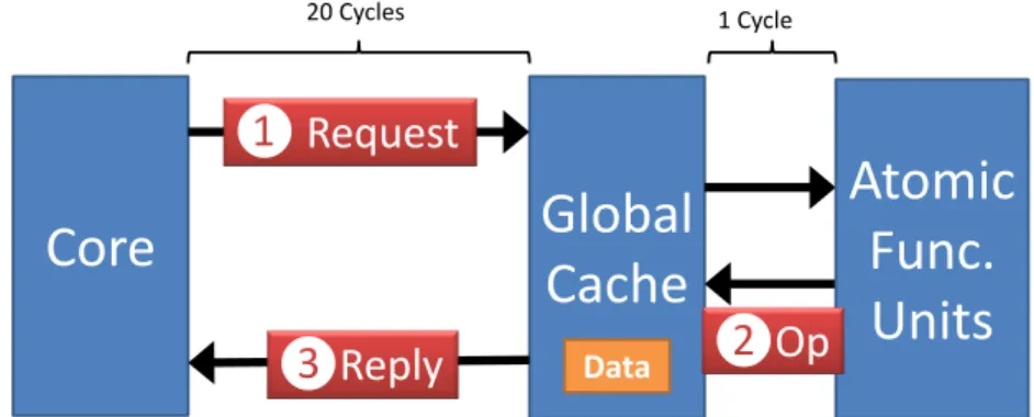
Global loads, stores, and atomics on Rigel always bypass core-level and cluster caches and complete at the last-level global cache. Memory locations operated on solely by global memory operations are trivially kept coherent across the chip because they may be cached in only a single location. Global operations are key to supporting synchronization, fine-grained inter-cluster communication and data sharing, system software features, and resource management. The cost of global memory operations is high compared to local operations due to increased latency, reduced read and write bandwidth, and contention on the shared global interconnect.
Rigel also implements a set of atomic operations (arithmetic, bitwise, min/max, exchange) that complete at the global cache.
2.3.3
Coherence
A key design consideration for a 1024-core accelerator processor is what the memory system should look like, including coherence. In analyzing the data sharing and communication patterns of visual computing workloads, we
ob-serve that such patterns can be leveraged in the design of memory systems for future manycore accelerators. Based on these insights, we developed both software and hardware mechanisms to manage coherence on parallel accelerator processors. We developed the Task-Centric Memory Model [5], a software protocol which works in concert with hardware caches to main-tain a coherent, single-address-space view of memory without the need for hardware coherence. We then developed Cohesion [6] as a mechanism to support hybrid coherence with both hardware and software-managed cache coherence features, enabling multiple memory models in heterogeneous or accelerator-based systems.
In the baselineRigel architecture, software must enforce coherence when inter-cluster read-write sharing exists. Coherence enforcement may be ac-complished by colocating sharers within a single coherent cluster, by using global memory accesses for shared data, or by forcing the writer to explicitly flush shared data before allowing the reader to access it. Explicit instructions for actions such as flushing and eviction are provided for cache management. Colocating sharers is not always possible, and using global accesses for all shared data is undesirable for performance reasons, because global cache and interconnect bandwidth is more limited. Instead, we develop a software algorithm to maintain coherence in a coarse-grained manner.
The cache coherence mechanism on Rigel is not implemented in hard-ware, but instead exploits the sharing patterns present in accelerator work-loads to enforce coherence in software. The sharing patterns present in our target workloads allow Rigel to leverage local caches for storing output write data between barriers before lazily making modifications globally visi-ble. Most data sharing on accelerator workloads occurs not between barriers but across barriers. Lazy updates can be performed as long as coherence ac-tions performed to write-output data are completed when a barrier is reached. Rigel enables software management of cache coherence in two ways. First, by providing instructions for explicit cluster cache management that include cache flushes and invalidate operations. Explicit cluster cache flushes up-date the value at the global cache, but do not upup-date or invaliup-date cached copies that may be held by other clusters. Second, broadcast invalidation and broadcast update operations allow software to implement data synchro-nization and wakeup operations that rely on invalidation or update-based
The topic of coherence is explored in more detail in Chapter 3.
2.4
Programming
Rigel
: The
Rigel
Task Model
Rigel is not restricted to running software written in a particular hardware-specific paradigm, but instead has the ability to run standard C code. We target Rigel using the LLVM compiler framework and a custom backend.
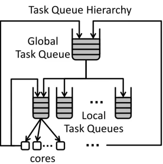
Rigel applications are developed using the Rigel Task Model (RTM), a simple bulk-synchronous parallel (BSP)[13], task-based work distribution library that we have developed. We implement task management primarily in software using hierarchical queues, enabling flexibility in work distribution and scheduling policies, and using minimal specialized hardware in the form of atomics, global memory accesses, and broadcasts.
Applications are written in RTM using a SPMD execution paradigm where all cores execute a single shared binary, but with arbitrary control flow per core. The programmer defines parallel work units, referred to as tasks, that are managed via queues by the RTM runtime. All threads may both enqueue and deque work at any time.
We define aninterval as the time between two global synchronization barri-ers. During an interval, worker threads can both produce and consume work units. There is no specified execution ordering for tasks within an interval. RTM task queues act as barriers when empty to provide global synchroniza-tion points. When a worker thread attempts to dequeue new work and finds an empty queue, the thread continues to poll for additional work. When all threads have reached this state and no additional work remains, a barrier has been reached. The last thread to enter the barrier notifies the remaining threads. For Rigel, barriers represent a point at which any locally cached non-private data should be flushed and made globally coherent before the start of a new interval. Figures 2.3 and 2.4 illustrate the BSP model we implement along with our hierarchical task queues.
Communication
Execution
Barrier
Task Execution
Idle Time
Ti meIn
te
rv
al
…
…
Local
Task Queues
Global
Task Queue
cores
…
Task Queue Hierarchy
Figure 2.3: The Rigel Task Model consists of hierarchical task queues. Depending on the configuration, cores may produce tasks into either local or global queues. Groups of tasks are removed from the global queue and placed into local queues for faster access and less contention.
Communication
Execution
Barrier
Task Execution
Idle Time
Ti
me
In
te
rv
al
…
…
Local
Task Queues
Global
Task Queue
cores
…
Task Queue Hierarchy
Figure 2.4: The BSP execution model of the Rigel Task Model. An interval is defined as the time between two barriers.
GCache 30mm2 (10%) Other Logic 30mm2 (9%) Overhead 53mm2
(17%) Cluster Cache SRAM
75mm2 (23%) Logic (Core+Cache) 112mm2 (35%) Register Files 20mm2 (6%) Clusters 207mm2 (67%)
Figure 2.5: Area estimates for the Rigel design.
2.5
Evaluation: Area and Power
To demonstrate feasibility of Rigel on current process technology, we pro-vide area and power estimates on a commercial 45 nm process. Our estimates are derived from synthesized Verilog, compiled SRAM arrays, IP compo-nents, and die plot analysis of other 45 nm designs. Core pipeline area is estimated from a functionally correct synthesized RTL model, including a single-precision floating-point unit. SRAM estimates are based on macros generated by a commercial memory compiler. Memory controller estimates are based on die plot analysis.
Figure 2.5 shows a breakdown of area estimates for the Rigel design. Cluster caches are 64 kB each and global cache banks total 4 MB. “Other Logic” encompasses interconnect as well as memory controller and global cache controller logic. For a conservative estimate, we include a 20% charge for additional overheads to account for some underestimation. The resulting 320 mm2 is reasonable for implementation in current process technologies,
and leaves space for additional SRAM cache, double-precision floating-point units, or more aggressive memory controllers.
Typical power consumption of the design with realistic activity factors for all components at 1.2 GHz is expected to be in the range of 99 W, though peak power consumption beyond 100 W is possible at high utilization. Our estimate is based on power consumption data for compiled SRAMs, postsyn-thesis power reports for logic, leakage, and clock tree of cluster components, estimates for interconnect and I/O pin power, and a 20% charge for addi-tional power overhead. The figure is similar to modern GPUs from NVIDIA
Table 2.3: Description of our data- and task-parallel workloads Benchmark Description
cg Conjugate gradient linear solver dmm Blocked dense matrix multiplication
fft 2D complex-to-complex radix-2 fast Fourier transform gjk Gilbert-Johnson-Keerthi 3D collision detection
heat 2D 5-point iterative, out-of-place stencil computation kmeans K-means clustering
march Marching cubes polygonization of 3D volumetric data mri Magnetic resonance image reconstruction (FHD matrix) sobel Sobel edge detection
stencil 3D 7-point iterative, out-of-place stencil computation
which consume around 150 W [14], while modern high-end CPUs can con-sume nearly as much.
2.6
Evaluation: Scalability
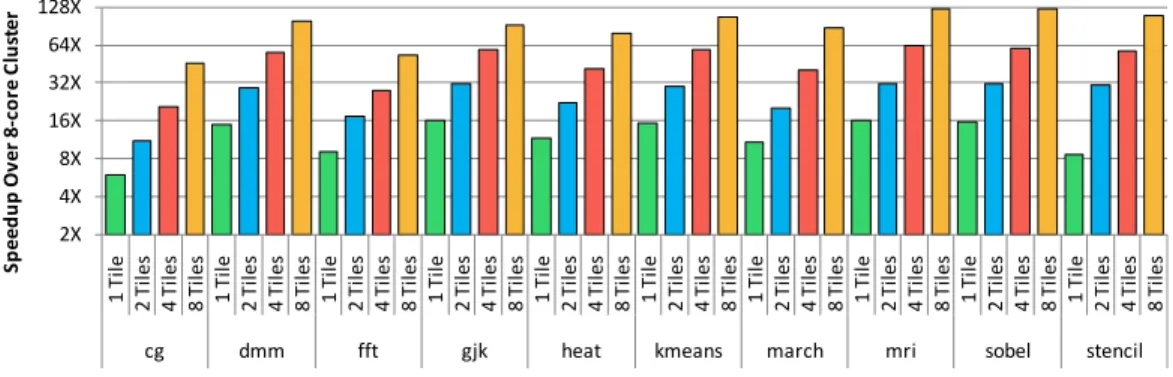
We evaluate Rigel based on a variety of parallel applications and kernels drawn from visual and scientific computing. Most benchmarks are written in a bulk-synchronous style using RTM for dynamic work distribution, but stencilstatically allocates work to threads. While all of our applications ex-hibit abundant data parallelism, the structure varies from dense (dmm,sobel) to sparse (cg) to irregular task-parallel (gjk) and includes diverse communi-cation patterns (kmeans,fft,heat,stencil). Table 2.3 describes our set of benchmark codes.
Figure 2.6 shows the kernel scalability for a variety of parallel applications up to 1024 cores. Across our selection of benchmarks, we observe an average speedup of 84× (harmonic mean) at 1024 cores compared to one eight-core cluster (128× speedup is ideal).
2.7
VLSI Implementation and Test Chip
The original goal of the Rigel project was to design and develop an archi-tecture that was implementable in contemporary fabrication process
tech-2X 4X 8X 16X 32X 64X 128X 1 T il e 2 Ti le s 4 Ti le s 8 T ile s 1 Ti le 2 T ile s 4 T ile s 8 Ti le s 1 T il e 2 T ile s 4 Ti le s 8 T ile s 1 Ti le 2 Ti le s 4 T ile s 8 Ti le s 1 Ti le 2 T ile s 4 Ti le s 8 T ile s 1 T il e 2 Ti le s 4 T ile s 8 T ile s 1 Ti le 2 T ile s 4 Ti le s 8 Ti le s 1 T il e 2 Ti le s 4 Ti le s 8 T ile s 1 Ti le 2 T ile s 4 T ile s 8 Ti le s 1 T il e 2 T ile s 4 Ti le s 8 T ile s
cg dmm fft gjk heat kmeans march mri sobel stencil
Sp eed u p O ver 8 -c o re C lu st er
Figure 2.6: Benchmark scalability on Rigel with 1, 2, 4, and 8 128-core tiles (128, 256, 512, and 1024 cores). Speedups are relative to a single eight-core cluster. 128×represents linear scaling at 1024 cores. Benchmark binaries and datasets are identical across all system sizes Global cache resources and memory controllers (and thus memory bandwidth) are scaled with the number of tiles.
architectural research ideas to be explored along with the full software and application stack to be explored on real hardware. Such a test platform was envisioned to enable interaction with domain experts in a more productive relationship than severely performance-limited simulation allows.
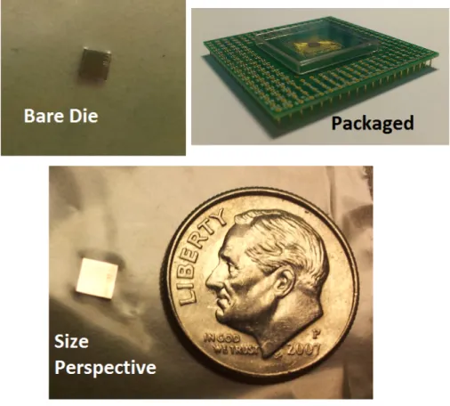
While the original goal of a full-scaleRigel test vehicle was not achieved, our fledgling RTL implementation was taped out in much smaller form as a 90 nm multicore processor. Figure 2.7 illustrates the fabricated die, both bare and packaged, and provides a scale comparison with a dime.
Though this test chip does not enable the original grand vision for a mas-sively parallel hardware platform for architecture and software research, it represents a significant achievement for the small number of students who enabled the project. It also provides validation of the underlying design and implementation that were used as the foundations of area and power esti-mates for the full Rigel design. Unfortunately, the older 90 nm process coupled with a design tuned for a newer process mean that actual area and power data from the test chip are not very applicable to the 45 nm intended design point. To fit within the constrained footprint, much smaller SRAMs were selected for caches, and an on-chip main memory array was added due to lack of proper memory controllers.
Table 2.4 enumerates some key parameters of the test chip. The test chip implemented a pair of reducedRigelclusters with two cores each for a total of four cores. Each core has independent L1 instruction and data caches.
Figure 2.7: Bare and packaged test chip die. The bare die is shown next to a dime for size comparison.
Table 2.4: Rigel test chip characteristics
Process Technology TSMC 90 nm
Die Area 3×32 mm
Frequency ˜125 MHz
Power Supply 1.0 V
Power Consumption (estimated) 100 to 230 mW
Cores 4 SRAM 16 kB cluster cache 0 6% cluster cache 1 6% main memory 19% I/O port 25% pipeline 0 11% pipeline 1 11% pipeline 2 11% pipeline 3 11% Pipelines 44%
Figure 2.8: Area breakdown data for the test chip implementation. Each cluster has a shared L2 cluster cache. For the test chip, an on-chip SRAM array serves as main memory. Figures 2.8 and 2.9 break down the estimated area and power for the test chip based on results from synthesis, place and route.
Figure 2.7 illustrates the fabricated die, both bare and packaged, and pro-vides a scale comparison with a dime. Figure 2.10 shows a wireplot. Fig-ure 2.11 shows a die plot of the test chip and labels key large blocks, including cores and caches. The chip was taped out in TSMC 90 nm technology in 2012, and as of this writing awaits bringup testing.
clock tree 7% cluster cache 0 4% cluster cache 1 4% main memory 10% I/O port 19% pipeline 0 14% pipeline 1 14% pipeline 2 14% pipeline 3 14% Pipelines 56%
Figure 2.9: Test chip power estimate breakdown.
CHAPTER 3
RIGEL MEMORY SYSTEM
Memory system considerations played a key role in the development of the Rigel architecture and programming model. The nature of the Rigel ac-celerator architecture led to the development of several novel elements of the memory system.
A high-performance accelerator requires efficient mechanisms for safely sharing data. In cached architectures, programmers must be able to safely share data between multiple caches in a reliable and predictable manner. Traditionally, hardware cache coherence mechanisms enable such sharing. While scalable multiprocessor hardware coherence schemes exist, they were envisioned for machines with drastically different mixes of computation, com-munication, and storage resources than large scale chip multiprocessors such as Rigel.
First, we consider the coherence requirements for accelerator systems and workloads. We examine a variety of parallel workloads and observe common data sharing and communication patterns. We show that for a variety of accelerator workloads, regular and clearly defined data sharing patterns exist. Our target applications exhibit more structured data sharing patterns than those applications targeted by traditional systems.
These observations motivate our initial design goal for Rigel, to achieve both good performance and ease of programmability without hardware co-herent caches. We find that we can leverage these characteristics to move the burden of coherence management from hardware to software. To this end, we introduce the Task-Centric Memory Model [5, 11], a software pro-tocol that enables the programmer to maintain coherence with incoherent hardware caches.
While we show that coherence is not strictly required for good perfor-mance or ease of programmability for accelerators such as Rigel, hardware cache coherence nonetheless retains attractive benefits. We developed
Co-hesion [6, 12], a hybrid memory model to bridge hardware and software coherent models.
Finally, we describe lazy atomics operations, an extension to TCMM that takes advantage of incoherent hardware caches for improved atomic operation bandwidth.
This chapter is organized as follows. Section 3.1 describes observations on parallel application characteristics, including parallelism structure and sharing patterns. Section 3.2 describes the Task-Centric Memory Model. Section 3.3 describes hybrid hardware-software coherence with Cohesion. Section 3.4 describes lazy atomic operations.
3.1
Parallel Application Characterization
Accelerators impose different constraints on caches and coherence manage-ment than traditional general purpose chip multiprocessors. An opportunity exists, driven by the characteristics of parallel accelerator workloads, to ex-ploit these differing constraints. The design of the Rigel memory system is influenced by the sharing and communication patterns of parallel workloads targeted by accelerators. We consider two sets of applications developed for two different platforms, x86/pthreads and Rigel/RTM. We find that struc-tured, coarse-grained sharing is common and that most sharing takes place across global synchronization points (barriers). We also find that fine-grained data sharing between barriers is relatively uncommon.
Figure 3.1 illustrates the types of sharing patterns studied and defines the terms we use here: input, output, private, and conflict. Figure 3.2 illustrates the sharing patterns in a set of parallel x86 workloads, while Figure 3.3 il-lustrates similar patterns in several workloads running on Rigel.
3.1.1
Parallelism Structure
We observe that the programming styles adopted by developers for parallel accelerator applications often share a bulk synchronous structure [13]. Paral-lel applications are composed of a collection of concurrently executing, mostly unordered tasks operating on mostly data-parallel work units. We define an interval as the time period between two barriers. We find that tasks share
Barrier Barrier conflicts output input private
Figure 3.1: We define an interval as the time between two barriers. Each arrow represents an independent task. Input reads and output writes communicate data across barriers. Conflict accesses share data between two tasks in the same barrier interval. Reads and writes private to a task include stack acceses and temporary data structures.
minimal data within intervals. Instead, at barriers, modified state is made globally visible for the next interval of computation.
Updates made by a task within an interval can generally only be assumed to be visible after the current interval has completed. Sharing modified data within an interval requires explicit synchronization by the programmer. In a barrier-synchronized, mostly-data-parallel, task-based shared-memory pro-gramming model, coherence management is required to enable sharing; how-ever, the mechanisms found in conventional CMP architectures to support arbitrary sharing through cache coherence are of marginal utility.
We observe that popular programming models used for developing large-scale data-parallel applications do not depend on the hardware support for arbitrary sharing provided by conventional systems. However, a mechanism for enabling some data, such as task queues or shared data structures, to be shared is required. Second, the common structure present in these parallel applications is rooted in the programmer’s attempt to create scalable code in a manner that is conceptually simple; thus there is minimal sharing.
3.1.2
Sharing Patterns
Our next observation is that emerging applications targeting accelerator sys-tems have common data sharing and synchronization characteristics that can
Figure 3.2: Read and write sharing between independent tasks in the VISBench suite [15]. 0% 10% 20% 30% 40% 50% 60% 70% 80% 90% 100% Wr ite Rea d Wr ite Rea d Wr ite Rea d Wr ite Rea d Wr ite Rea d Wr ite Rea d Wr ite Rea d
CG DMM GJK HEAT KMEANS MRI SOBEL
Output Conflict Private Input
Figure 3.3: Characterization of memory accesses in task-based BSP applications. Inputreads and output writes communicate data across barriers. The majority of memory accesses are to data that is private to a task. Conflict accesses share data between two tasks in the same barrier interval, requiring hardware coherence or synchronization mechanisms such as atomic operations to maintain correctness, but are rare in our
guide the design of future accelerator architectures. We provide analysis of a set of parallel visual computing workloads from VISBench [15] and from the Rigel kernel benchmark suite. VISBench consists of a set of full applications that we run on the x86 platform. The Rigel benchmarks conjugate gradient solver (CG), Sobel edge detection, k-means clustering, and dense matrix mul-tiply (DMM) were written by hand and optimized for the Rigel architecture. GJK collision detection was ported from a freely available sequential version. Heat is ported from the Cilk [16] benchmark with optimizations applied for Rigel. MRI benchmark is a port of the VISBench medical imaging code.
Analysis of these workloads shows similar data sharing and synchronization patterns. Specifically, we investigate the sharing patterns of our workloads with respect to synchronization boundaries. Figure 3.1 illustrates the types of sharing patterns studied and illustrates the terms we use here: input, output, private, and conflict. Figure 3.2 shows the number of unique memory references that are shared across intervals, marked as input and output, and within an interval, marked as conflict, for VISBench applications. Figure 3.3 shows the same for the Rigel benchmark suite. Note that the results for MRI differ due to register spilling on x86, resulting in more private reads and writes (to the stack) on x86 compared to Rigel. We exclude work distribution related sharing from results to highlight application-level characteristics.
Figures 3.2 and 3.3 show the frequency of non-private loads and stores, which are data produced by one task and consumed by one or more other tasks. Non-private accesses are further broken down by whether values are shared between tasks within an interval, which we call conflict reads and writes, or across intervals, which we call input readsand output writes. The figures show that the majority of non-private loads are to data produced before the current interval began (input reads). At the same time, both conflict reads and writes to data shared within an interval are rare. Output writes, which are writes by a task in the current interval consumed by one or more tasks in the next interval, are more common in real applications than true shared writes, which require intra-interval synchronization; moreover, they constitute a small fraction of overall execution. Also note that the number of unique output writes is much smaller than the number of input reads in the figure due to one-to-many sharing across intervals.
3.1.3
Accelerator Workload Characteristics
We observe five common characteristics in accelerator workloads:
1. Large amounts of immutable, read-shared data are present within an interval. Examples of read-shared data from our workloads include input images and video or scene and model description data.
2. Synchronization is coarse grained. This in turn motivates our investi-gation of bulk coherence management at task boundaries. Indicative of this pattern are output writes and corresponding input reads in Fig-ure 3.2 and FigFig-ure 3.3, which demonstrate that modified data is often read by a task after the interval in which the data was written has ended.
3. There exists only small amounts of write-shared data within an inter-val, which indicates that tasks are highly data-parallel with few data dependences between tasks within an interval. The lack of data depen-dences is illustrated in Figure 3.2 and Figure 3.3 as a lack of conflict reads and writes. The conflicts that do exist are structured, such as the histogramming operations in k-means and the reduction operations in CG.
4. Fine-grained synchronization is present but rare. An example of such synchronization is atomic updates to shared data structures. We ob-serve that much of the fine-grained synchronization that we do find is used for task management and not for application code.
5. When write sharing within an interval does exist, it is usually between few sharers.
Collectively, these characteristics demonstrate that little coherence man-agement is required within an interval, indicating the potential for pushing coherence management into software to be logically performed at the end of an interval. At the same time, mechanisms must be present to enable small amounts of fine-grained synchronization and data sharing within an interval and to support task management efficiently. Our findings further motivate the use of shared caches that can amortize the costs associated with data ac-cess to read-shared data, a prevalent acac-cess pattern in our target workloads.
3.2
Software-managed Coherence with the
Task-Centric Memory Model
3.2.1
The Task-Centric Memory Model
Adopting a structured programming model enables us to implement software-managed cache coherence efficiently. We developed the Task-Centric Memory Model (TCMM) [5] as a contract describing the software actions necessary to ensure correctness in task-based BSP programs in the absence of hardware-enforced coherence.
Figure 3.4 illustrates the state transitions for a cacheline in our protocol. All blocks start in the clean state with no sharers or cached copies and may transition to immutable (read-only), shared as globally coherent, or private. State is implicit and must be tracked by the programmer. Cachedlocal memory operations may operate onprivateorimmutabledata, whereas uncached global operations are required for globally coherent data. Transitioning data between states requires first moving through the clean state.
Software cache coherence requires minimal hardware support in the form of instructions for explicitly writing back and invalidating data in private caches. We found that a small number of additional hardware mechanisms, such as broadcast support to accelerate global barriers and global atomic op-erations to facilitate infrequent intra-barrier sharing, greatly improved scal-ability over a na¨ıve design. With these relatively inexpensive mechanisms, TCMM was able to achieve performance within a few percent of idealized hardware coherence at 1024 cores. Future accelerators may improve upon TCMM by automating coherence actions in the compiler and scheduling co-herence actions to maximize cache locality.
3.2.2
Performance Evaluation
A simple implementation of TCMM which strictly adheres to the actions as described potentially requires large numbers of writebacks and invalidates at task boundaries. This flurry of traffic at task boundaries can cause conges-tion in the memory system and interfere with tasks performing useful work.
Immutable
Globally
Coherent
Private
(Dirty)
Clean
ε
Private
(Clean)
Inv L.LD L.LD L.ST WB L.LD, L.ST G.LD,G.ST,INV G.LD, G.ST L.LD, Inv L.LDε
Figure 3.4: State transitions for a cacheline under control of the
Task-Centric Memory Model protocol. G indicates global operations, L local operations, WB writebacks, INVinvalidates, no sharers, LD loads, and ST stores.
0.0x 0.2x 0.4x 0.6x 0.8x 1.0x
cg dmm heat kmeans mri sobel
Spe edup v s. Ide al H W Co he re nc e
LILW
LIEW
EILW
EIEW
Figure 3.5: Performance of TCMM for four policy combinations of
eager/lazy and invalidation/writeback relative to ideal (zero-cost) hardware coherence.
At the same time read-only data may be needlessly flushed, reducing the effectiveness of caching for read shared immutable data.
Coherence actions are not strictly required to be issued at task boundaries, Coherence actions can be deferred until the end of an interval to improve performance depending on task behavior. We definelazy actions to take place when a barrier is reached, while eager actions take place immediately upon task completion. We consider combinations of both eager and lazy writebacks and invalidates. For different applications or classes of data, different policies may be optimal.
Figure 3.5 compares performance of each policy selection for TCMM to an idealized baseline of zero-cost hardware coherence. The results show eager in-validate/eager writeback (EIEW), lazy invalidate/ eager writeback (LIEW), eager invalidate/lazy writeback (EILW), and lazy invalidate/lazy writeback (LILW) relative to the optimistic baseline.
We see that different policy combinations may be optimal for each appli-cation, highlighting the power of flexibility in software. Applications may be tuned and select a policy optimized for their memory access patterns, rather than relying upon a hardware default. Only MRI suffers a penalty of greater than 10% vs. the idealized baseline. Eager writebacks overlap write traffic with task execution, improving memory system utilization, as can be seen with . At the same time, lazy invalidation for read-shared data can
improve cache effectiveness for data that is read again by other tasks. The TCMM protocol is described in more detail along with additional performance analysis in [5].
3.3
Hybrid Coherence with
Cohesion
Memory models in use today are either fully hardware-coherent or fully software-coherent. In systems that include both models, the two models are strictly separated by using disjoint address spaces or physical memories. As systems-on-chip (SoCs) and other heterogeneous platforms become more prevalent, the ability to seamlessly manage data across different memory models will become increasingly important.
Software-managed cache coherence (SWcc) removes the area, power, and interconnect traffic overhead of cache coherence for structured data sharing patterns and allows experienced application developers to achieve high per-formance. Hardware coherence (HWcc) avoids the instruction overhead of software coherence, performs well with unstructured sharing patterns, and provides correct data sharing with low programmer effort. To achieve the combined benefits of these two models, we have developed Cohesion, a hybrid memory model.
Figure 3.6 illustrates the high-level operation ofCohesion. Cohesion in-cludes a hardware coherence implementation which tracks the entire address space by default. The developer can selectively remove cache lines from the hardware coherent domain at runtime and manage them using software to improve performance. Because data can move back and forth between the software coherent and hardware coherent domains at will, Cohesioncan be used to dynamically adapt to the sharing needs of applications and runtimes and does not require multiple address spaces nor explicit copy operations. Cohesion can also enable the integration of multiple memory models in heterogeneous or accelerator-based systems such as SoCs. We implement software-managed coherence using TCMM and use an MSI-based hardware coherence protocol, but any hardware and software protocols may be used so long as the necessary state transitions are enforced.
Figure 3.7 illustrates the hardware structures that implement Cohesion. A directory tracks shared words in theHWccdomain. The coarse-grain region
4/18/2011 1 T=0 T=1 T=2 T=3 T=4 0x100 0x140 0x160 0x180 0x1C0 … 0x120 0x1A0
SW‐managed Coherence Protocol HW‐managed Coherence Protocol
SW-to-HWTransitions
C
OHESIONSWccCache Line
HWccCache Line Transition
Addr ess Space Time Immutable Globally Coherent Private (Dirty) Clean ε Private (Clean) Inv L.LD L.LD L.ST WB L.LD, L.ST G.LD,G.ST,INV G.LD, G.ST L.LD, Inv L.LD ε
Figure 3.6: Cohesionis a hybrid memory model for accelerators that enables hardware and software-managed coherence to coexist, allowing data to migrate between the two domains dynamically. Left: State transitions for a cacheline under control of the Task-Centric Memory Model protocol. G indicates global operations, L local operations, WB writebacks, INV invalidates, no sharers, LD loads, and ST stores.
code segment stack segment … wm-1 wm-2 w0 w1 set0 set1 setn-2 setn-1
sharers tag I/M/S
global data Coherence bit vectors (1 bit/line) 16 MB table/ 4 GB memory base_addr
start_addr size valid
Sparse Directory
Coarse-grain Region Table
Fine-grain Region Table
(One per L3 bank) (Global Table) (Strided across L3 banks)
Figure 3.7: Cohesion hardware architecture.
table tracks large regions of memory within the SWcc domain, such as code, an incoherent heap, or private stack space. Finally, the fine-grain region table tracks the rest of memory that may transition dynamically between the two domains. Each L2 cache keeps a per-line incoherent bit to track lines which are not under the control of hardware coherence.
When a request arrives, the directory is first queried to determine if the line is under hardware management. If so, the access is handled as is typical under the hardware coherence protocol. If the line is not present in the directory, the region tables are queried next. If the address maps to the coarse-grain region table, the access proceeds without intervention from the hardware coherence protocol, and the incoherent bit is set on the response. If the address does not map to either the directory or the coarse-grain region table, the fine-grain region table is checked. The fine-grain region table is a
0K 50K 100K 150K 200K 250K 300K Coh es ion H Wc c Coh es ion H Wc c Coh es ion H Wc c Coh es ion H Wc c Coh es ion H Wc c Coh es ion H Wc c Coh es ion H Wc c Coh es ion H Wc c Coh es ion H Wc c
CG DMM GJK HEAT KMEANS MRI SOBEL STENCIL Mean
A ver ag e # D ir ec to ry E nt ri es A llo ca ted
Code Heap/Global Stack Maximum Allocated 0.0x 1.0x 2.0x 3.0x 4.0x 5.0x 6.0x 7.0x 8.0x 256 512 1024 2048 4096 8192 16384 Directory Entries per L3 Cache Bank
cg dmm gjk heat kmeans mri sobel stencil 0.0x 1.0x 2.0x 3.0x 4.0x 5.0x 6.0x 7.0x 8.0x 256 512 1024 2048 4096 8192 16384 Sl ow do w n N or m al iz ed to In fin it e En tr ie s
Directory Entries per L3 Cache Bank
(B)
(C)
(A)
Figure 3.8: Performance versus directory cache size for (A) HWcc alone and (B) Cohesion, which amplifies effective directory size by moving some data from HWcc toSWcc.
cached data structure that stores one state bit per cacheline which indicates membership in eitherHWcc orSWcc. If the line is underSWcc, an incoherent access is initiated. If the line is under HWcc, a directory entry is allocated for hardware tracking and a coherent access is initiated.
A developer may instruct the hardware coherence machinery to defer to software management for a particular cache line by updating a software-accessible table in memory. For instance, hardware coherence management is inefficient when data is private or when a large amount of data can be man-aged as a unit by software. Handling read-mostly and private data outside the scope of the hardware coherence protocol can increase performance and reduce the load on the coherence hardware, increasing the effective directory size for data managed under hardware coherence, as seen in Figure 3.8.
Ultimately, Cohesionallows explicit coherence management to be an op-tional optimization opportunity, rather than necessary for correctness. Co-hesion is explored in greater detail in [6, 12].
3.4
Lazy Atomic Operations
We have considered the need for cache coherence in accelerator architectures and described efficient mechanisms for managing coherence in software with
incoherent hardware caches via the Task-Centric Memory Model. While the TCMM work was focused on enforcing coherence, we now consider taking advantage of incoherent hardware caches in a novel way to improve perfor-mance. We introducelazy atomic operations, a hardware mechanism targeted at throughput processors that leverages incoherent hardware caches to trans-parently improve throughput for order-independent atomic operations while simultaneously improving the ease of programming. This work was originally published in [17].
Both GPUs and CPUs implement atomic operations, popular in throughput-oriented GPGPU computing with languages such as CUDA [18] and Open-CL [19]. Atomic operations are important in parallel codes for massively parallel accelerators such as Rigelor GPUs and have a wide variety of uses in parallel applications. Algorithms in scientific computing, data mining, and image processing make use of atomic updates, including k-means clustering, principle component analysis (PCA), sorting, convex hull, histogramming, two-point angular correlation function (TPACF), and even SQL databases.
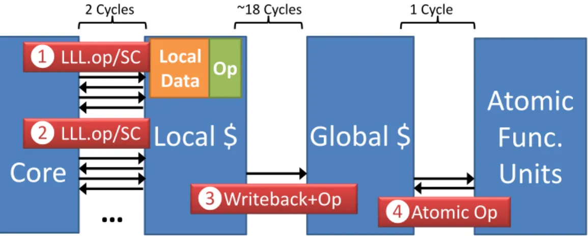
In a parallel system, throughput of atomic operations is limited due to the serializing nature of atomic operations and limited atomic hardware units. Global atomics are especially easy to use for programmers, but suffer from orders of magnitude lower throughput and higher latency than local opera-tions. While local atomic operations may be available, using them can require more c
![Figure 3.2: Read and write sharing between independent tasks in the VISBench suite [15]](https://thumb-us.123doks.com/thumbv2/123dok_us/1080921.2643794/38.918.177.744.137.453/figure-read-write-sharing-independent-tasks-visbench-suite.webp)
![Figure 3.14: State diagram for cache line transitions. This is an extended version of the TCMM protocol originally described in [5].](https://thumb-us.123doks.com/thumbv2/123dok_us/1080921.2643794/53.918.248.739.115.344/figure-diagram-transitions-extended-version-protocol-originally-described.webp)