New Multilevel Inverter D-STATCOM Topology To Compensate
Reactive And Nonlinear Loads
Kollu Suresh Kumar*1J Ramesh2
M.Tech Student, Department of EEE, KIET-II, KakinadaIndia.1 Asst. Professor, Department of EEE, KIET-II, Kakinada, India.2
Abstract— This work proposes an enhanced half and half dissemination static compensator (D-STATCOM) topology to address some reasonable issues, for example, control rating, channel measure, remuneration execution, and power misfortune. A LCL channel has been utilized at the front end of a voltage source inverter (VSI), which gives better exchanging music disposal while utilizing substantially littler estimation of an inductor as contrasted and the conventional L channel. A capacitor is utilized as a part of arrangement with a LCL channel to diminish the dc-connect voltage of the D-STATCOM. This thus diminishes the power rating of the VSI. With decreased dc-connect voltage, the voltage over the shunt capacitor of the LCL channel will be additionally less. It will lessen the power misfortunes in the damping resistor as contrasted and the customary LCL channel with inactive damping. In this way, the proposed DSTATCOM topology will have lessened weight, cost, rating, and size with enhanced proficiency and current remuneration ability contrasted and the customary topology. An efficient technique to plan the parts of the aloof channel has been introduced. A multilevel fell H-extension is executed in the VSI operation of a D-STATCOM topology. The viability of the proposed DSTATCOM topology over customary topologies is approved through MATLAB/SIMULINK programming.
Index Terms—Distribution static compensator (DSTATCOM), multilevel inverter (MLI), fell H-connect, inactive channel, control quality (PQ).
I. Introduction
Customarily static capacitors and inactive channels have been used to enhance control quality (PQ) in a circulation framework. Nonetheless, these for the most part have issues, for example, settled pay, framework parameter-subordinate execution, and conceivable reverberation with line reactance [2]. A dissemination static compensator (DSTATCOM) has been proposed in the writing to defeat these disadvantages [3]–[8]. It infuses responsive and music part of load streams to make source ebbs and flows adjusted, sinusoidal, and in stage with the heap voltages. In any case, a customary
DSTATCOM requires a powerful appraising voltage source inverter (VSI) for load remuneration. The power rating of the DSTATCOM is specifically relative to the current to be repaid and the dc-connect voltage [10].Generally, the dc-interface voltage is kept up at substantially higher incentive than the most extreme estimation of the stage to-impartial voltage in a stage four-wire framework for tasteful pay (in a three-stage three-wire framework, it is higher than the three-stage to-stage voltage) [2], [10]–[12]. Be that as it may, a higher dc-interface voltage expands the rating of the VSI, makes the VSI substantial, and brings about higher voltage rating of protected door bipolar transistor (IGBT) switches. It prompts the expansion in the cost, size, weight, and power rating of the VSI. Likewise, conventional DSTATCOM topologies utilize a L-sort interfacing channel for molding of the VSI infused streams [13], [14]. The L channel utilizes an extensive inductor, has a low slew rate for following the reference streams, and delivers a substantial voltage drop crosswise over it, which, thusly, requires a higher estimation of the dc-connect voltage for appropriate pay.
Thusly, the L channel includes cost, size, and power rating. Some half breed topologies have been proposed to consider the previously mentioned impediments of the conventional DSTATCOM, where a diminished rating dynamic channel is utilized with the latent parts [15]–
[21]. In [15] and [16], cross breed channels for engine drive applications have been proposed. In [17], creators have accomplished a decrease in the dc-connect voltage for responsive load pay. In any case, the lessening in voltage is constrained because of the utilization of a L-sort interfacing channel. This likewise makes the channel greater in size and has a lower slew rate for reference following. A LCL channel has been proposed as the front end of the VSI in the writing to defeat the restrictions of a L channel [22]–[25]. It gives better reference following execution while utilizing much lower estimation of detached segments. This likewise decreases the cost, weight, and size of the uninvolved segment. Nonetheless, the LCL channel utilizes a comparable dc-interface voltage as that of DSTATCOM utilizing a L channel. Henceforth, burdens because of
New Multilevel Inverter D-STATCOM Topology To Compensate
Reactive And Nonlinear Loads
Kollu Suresh Kumar*1J Ramesh2
M.Tech Student, Department of EEE, KIET-II, KakinadaIndia.1 Asst. Professor, Department of EEE, KIET-II, Kakinada, India.2
Abstract— This work proposes an enhanced half and half dissemination static compensator (D-STATCOM) topology to address some reasonable issues, for example, control rating, channel measure, remuneration execution, and power misfortune. A LCL channel has been utilized at the front end of a voltage source inverter (VSI), which gives better exchanging music disposal while utilizing substantially littler estimation of an inductor as contrasted and the conventional L channel. A capacitor is utilized as a part of arrangement with a LCL channel to diminish the dc-connect voltage of the D-STATCOM. This thus diminishes the power rating of the VSI. With decreased dc-connect voltage, the voltage over the shunt capacitor of the LCL channel will be additionally less. It will lessen the power misfortunes in the damping resistor as contrasted and the customary LCL channel with inactive damping. In this way, the proposed DSTATCOM topology will have lessened weight, cost, rating, and size with enhanced proficiency and current remuneration ability contrasted and the customary topology. An efficient technique to plan the parts of the aloof channel has been introduced. A multilevel fell H-extension is executed in the VSI operation of a D-STATCOM topology. The viability of the proposed DSTATCOM topology over customary topologies is approved through MATLAB/SIMULINK programming.
Index Terms—Distribution static compensator (DSTATCOM), multilevel inverter (MLI), fell H-connect, inactive channel, control quality (PQ).
I. Introduction
Customarily static capacitors and inactive channels have been used to enhance control quality (PQ) in a circulation framework. Nonetheless, these for the most part have issues, for example, settled pay, framework parameter-subordinate execution, and conceivable reverberation with line reactance [2]. A dissemination static compensator (DSTATCOM) has been proposed in the writing to defeat these disadvantages [3]–[8]. It infuses responsive and music part of load streams to make source ebbs and flows adjusted, sinusoidal, and in stage with the heap voltages. In any case, a customary
DSTATCOM requires a powerful appraising voltage source inverter (VSI) for load remuneration. The power rating of the DSTATCOM is specifically relative to the current to be repaid and the dc-connect voltage [10].Generally, the dc-interface voltage is kept up at substantially higher incentive than the most extreme estimation of the stage to-impartial voltage in a stage four-wire framework for tasteful pay (in a three-stage three-wire framework, it is higher than the three-stage to-stage voltage) [2], [10]–[12]. Be that as it may, a higher dc-interface voltage expands the rating of the VSI, makes the VSI substantial, and brings about higher voltage rating of protected door bipolar transistor (IGBT) switches. It prompts the expansion in the cost, size, weight, and power rating of the VSI. Likewise, conventional DSTATCOM topologies utilize a L-sort interfacing channel for molding of the VSI infused streams [13], [14]. The L channel utilizes an extensive inductor, has a low slew rate for following the reference streams, and delivers a substantial voltage drop crosswise over it, which, thusly, requires a higher estimation of the dc-connect voltage for appropriate pay.
Thusly, the L channel includes cost, size, and power rating. Some half breed topologies have been proposed to consider the previously mentioned impediments of the conventional DSTATCOM, where a diminished rating dynamic channel is utilized with the latent parts [15]–
International Journal of Science Engineering and Advance
Technology, IJSEAT, Vol. 5, Issue 5
ISSN 2321-6905
May -2017
high dc-interface voltage are as yet present when the LCL channel is utilized. Another significant issue is reverberation damping of the LCL channel, which may push the framework toward flimsiness. One arrangement is to utilize dynamic damping. This can be accomplished utilizing either extra sensors or sensor less plans. The sensor less dynamic damping plan is anything but difficult to execute by adjusting the inverter control structure. It disposes of the requirement for extra sensors. In any case, higher request computerized channels utilized as a part of these plans may require to be tuned for palatable execution [26]. Another approach is to go for detached damping. This does not require additional sensor hardware. Nonetheless, inclusion of a damping resistor in the shunt some portion of a LCL channel brings about additional power misfortune and diminishes the proficiency of the framework [26]. This paper proposes an enhanced cross breed DSTATCOM topology where the LCL channel taken after by the arrangement capacitor is utilized at the front end of the VSI to address the previously mentioned issues. This topology diminishes the extent of the detached parts and the rating of the dc-interface voltage and gives great reference following execution at the same time. Alongside this, a huge diminishment in the damping power misfortune is accomplished, which makes this plan reasonable for mechanical applications. The execution of the proposed topology is approved through the broad reenactment comes about.
II. PROPOSED DSTATCOM TOPOLOGY
A three-phase equivalent circuit diagram of the proposed DSTATCOM topology is shown in Fig. 1. It is realized using a three-phase four-wire two-level neutral-point-clamped VSI.
Fig.1. Proposed DSTATCOM topology in the distribution system to compensate unbalanced and nonlinear loads.
The proposed conspire interfaces a LCL channel at the front end of the VSI, which is trailed by an arrangement capacitor Cse. Presentation of the LCL channel essentially decreases the measure of the latent segment and enhances the reference following execution. Expansion of the arrangement capacitor decreases the dc-connect voltage and, along these lines, the power rating of the VSI. Here, R1 and L1 speak to the resistance and inductance, individually, at the VSI side; R2 and L2 speak to the resistance and inductance, separately, at the heap side; and C is the channel capacitance framing the LCL channel part in each of the three stages. A damping resistance Rd is utilized as a part of arrangement with C to soggy out reverberation and to give latent damping to the general framework. VSI and channel streams are if1a and if2a, individually, in stage an and comparable for different stages. Furthermore, voltages crosswise over and streams through the shunt branch of the LCL channel in stage an are given by Vsha and isha, individually, and comparably for the other two stages. The voltages kept up over the dc-connect capacitors are Vdc1 = Vdc2 = Vdcref . The DSTATCOM, source, and loads are associated with a typical point called the purpose of regular coupling (PCC). Loads utilized here have both straight and nonlinear components, which might be adjusted or lopsided. In the conventional DSTATCOM topology considered in this paper, the same VSI is associated with the PCC through an inductor Lf [27]. In the LCL channel based DSTATCOM topology, a LCL channel is associated between the VSI and the PCC [22].
IIa. MULTILEVEL INVERTER TOPOLAGIES
An inverter is an electrical gadget that believers coordinate current (DC) to substituting current (AC); the changed over AC can be at any required voltage and recurrence with the utilization of fitting transformers, exchanging, and control circuits. Static inverters have no moving parts and are utilized as a part of an extensive variety of uses, from little exchanging power supplies in PCs, to huge electric utility high-voltage coordinate current applications that vehicle mass power. Inverters are ordinarily used to supply AC control from DC sources, for example, sunlight based boards or batteries. The electrical inverter is a high-control electronic oscillator. It is so named in light of the fact that early mechanical AC to DC converters was made to work backward, and in this way were "rearranged", to change over DC to AC. The inverter plays out the inverse capacity of a rectifier. Sorts in multilevel inverter are examined underneath. There are three sorts of traditional multilevel inverters in particular diode braced, fell H-extension and flying capacitor.
International Journal of Science Engineering and Advance
Technology, IJSEAT, Vol. 5, Issue 5
ISSN 2321-6905
May -2017
high dc-interface voltage are as yet present when the LCL channel is utilized. Another significant issue is reverberation damping of the LCL channel, which may push the framework toward flimsiness. One arrangement is to utilize dynamic damping. This can be accomplished utilizing either extra sensors or sensor less plans. The sensor less dynamic damping plan is anything but difficult to execute by adjusting the inverter control structure. It disposes of the requirement for extra sensors. In any case, higher request computerized channels utilized as a part of these plans may require to be tuned for palatable execution [26]. Another approach is to go for detached damping. This does not require additional sensor hardware. Nonetheless, inclusion of a damping resistor in the shunt some portion of a LCL channel brings about additional power misfortune and diminishes the proficiency of the framework [26]. This paper proposes an enhanced cross breed DSTATCOM topology where the LCL channel taken after by the arrangement capacitor is utilized at the front end of the VSI to address the previously mentioned issues. This topology diminishes the extent of the detached parts and the rating of the dc-interface voltage and gives great reference following execution at the same time. Alongside this, a huge diminishment in the damping power misfortune is accomplished, which makes this plan reasonable for mechanical applications. The execution of the proposed topology is approved through the broad reenactment comes about.
II. PROPOSED DSTATCOM TOPOLOGY
A three-phase equivalent circuit diagram of the proposed DSTATCOM topology is shown in Fig. 1. It is realized using a three-phase four-wire two-level neutral-point-clamped VSI.
Fig.1. Proposed DSTATCOM topology in the distribution system to compensate unbalanced and nonlinear loads.
The proposed conspire interfaces a LCL channel at the front end of the VSI, which is trailed by an arrangement capacitor Cse. Presentation of the LCL channel essentially decreases the measure of the latent segment and enhances the reference following execution. Expansion of the arrangement capacitor decreases the dc-connect voltage and, along these lines, the power rating of the VSI. Here, R1 and L1 speak to the resistance and inductance, individually, at the VSI side; R2 and L2 speak to the resistance and inductance, separately, at the heap side; and C is the channel capacitance framing the LCL channel part in each of the three stages. A damping resistance Rd is utilized as a part of arrangement with C to soggy out reverberation and to give latent damping to the general framework. VSI and channel streams are if1a and if2a, individually, in stage an and comparable for different stages. Furthermore, voltages crosswise over and streams through the shunt branch of the LCL channel in stage an are given by Vsha and isha, individually, and comparably for the other two stages. The voltages kept up over the dc-connect capacitors are Vdc1 = Vdc2 = Vdcref . The DSTATCOM, source, and loads are associated with a typical point called the purpose of regular coupling (PCC). Loads utilized here have both straight and nonlinear components, which might be adjusted or lopsided. In the conventional DSTATCOM topology considered in this paper, the same VSI is associated with the PCC through an inductor Lf [27]. In the LCL channel based DSTATCOM topology, a LCL channel is associated between the VSI and the PCC [22].
IIa. MULTILEVEL INVERTER TOPOLAGIES
IIb. cascaded H-Bridges inverter
A solitary stage structure of a m-level fell inverter is shown in fig.2. Each different dc source (SDCS) is associated with a solitary stage full-scaffold, or H-connect, inverter. Every inverter level can produce three distinctive voltage yields, +Vdc, 0, and –Vdc by interfacing the dc source to the air conditioner yield by various mixes of the four switches, S1, S2, S3, and S4. To acquire +Vdc, switches S1 and S4 are turned on, though –Vdc can be gotten by turning on switches S2 and S3. By turning on S1 and S2 or S3 and S4, the yield voltage is 0. The air conditioner yields of each of the distinctive full-connect inverter levels are associated in arrangement to such an extent that the orchestrated voltage waveform is the aggregate of the inverter yields. The quantity of yield stage voltage levels m in a course inverter is characterized by m = 2s+1, where s is the quantity of partitioned dc sources. A case stage voltage waveform for a 11-level fell H-connect inverter with 5 SDCSs and 5 full extensions is appeared in figure. The stage voltage v
an= va1+ va2+ va3+ va4+ va5.
Fig 2 Single-phase structure of a multilevel cascaded H-bridges inverter
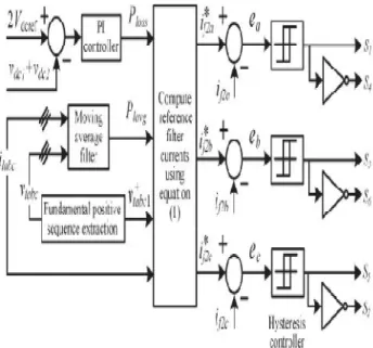
III. DSTATCOM CONTROL
The overall control block diagram is shown in Fig. 3. The DSTATCOM is controlled in such a way that the source currents are balanced, sinusoidal, and in phase with the respective terminal voltages. In addition, average load power and losses in the VSI are supplied by the source. Since the source considered. here is non stiff, the direct use of terminal voltages to calculate reference filter currents will not provide satisfactory compensation. Therefore, the fundamental positive sequence components of three-phase voltages are extracted to generate reference filter currents. The
equations required for the control of a D –Statcom analyzed through SRF theory with PI controller.(1)
Fig 3 Controller block diagram.
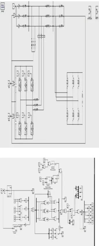
IV.SIMULATION CIRCUITS AND RESULTS
4.1 SIMULATION BLOCK DIAGRAM WITHOUT D-STATCOM/COMPENSATION:
International Journal of Science Engineering and Advance
Technology, IJSEAT, Vol. 5, Issue 5
ISSN 2321-6905
May -2017
dc capacitors, and also the aggregate dc-interface voltage, are introduced in Fig. 5(d). The voltage over every capacitor is kept up at 520 V, while the aggregate dc-connect voltage is kept up at 1040 V utilizing the PI controller. The source streams and PCC voltages are adjusted and sinusoidal however contain critical exchanging music swell. Their rate add up to symphonious twists (THDs) are given (1). To oblige control misfortunes in the damping resistor, the source streams are somewhat expanded contrasted and the conventional topology. Besides, the aggregate dc-interface voltage is kept up at 1040 V (same as the conventional plan) to accomplish stack pay.
4.2 SIMULATION RESULTS:
Fig.4.2 (a) wave form for Isa
Fig.4.2 (b) Source current:
Fig.4.2(C) PCC Voltage
4.3a Simulation Block Diagram With Proposed D- Statcom:
fig 4.3 (b) Control block diagram
International Journal of Science Engineering and Advance
Technology, IJSEAT, Vol. 5, Issue 5
ISSN 2321-6905
May -2017
dc capacitors, and also the aggregate dc-interface voltage, are introduced in Fig. 5(d). The voltage over every capacitor is kept up at 520 V, while the aggregate dc-connect voltage is kept up at 1040 V utilizing the PI controller. The source streams and PCC voltages are adjusted and sinusoidal however contain critical exchanging music swell. Their rate add up to symphonious twists (THDs) are given (1). To oblige control misfortunes in the damping resistor, the source streams are somewhat expanded contrasted and the conventional topology. Besides, the aggregate dc-interface voltage is kept up at 1040 V (same as the conventional plan) to accomplish stack pay.
4.2 SIMULATION RESULTS:
Fig.4.2 (a) wave form for Isa
Fig.4.2 (b) Source current:
Fig.4.2(C) PCC Voltage
4.3a Simulation Block Diagram With Proposed D- Statcom:
4.3.1 SIMULATION RESULTS:
Fig.4.3.1(a) Source currents
Fig.4.3.1(b) PCC voltages
Fig.4.3.1 (c) Voltage across the dc link
Fig.4.3.1 (e)Reduced Total Harmonic Distortion(4.96%)
Fig- 5.1 Simulink Block Diagram Of Proposed Topology
5.2 Source currents and PCC voltages
5.3 Filter voltages 4.3.1 SIMULATION RESULTS:
Fig.4.3.1(a) Source currents
Fig.4.3.1(b) PCC voltages
Fig.4.3.1 (c) Voltage across the dc link
Fig.4.3.1 (e)Reduced Total Harmonic Distortion(4.96%)
Fig- 5.1 Simulink Block Diagram Of Proposed Topology
5.2 Source currents and PCC voltages
5.3 Filter voltages 4.3.1 SIMULATION RESULTS:
Fig.4.3.1(a) Source currents
Fig.4.3.1(b) PCC voltages
Fig.4.3.1 (c) Voltage across the dc link
Fig.4.3.1 (e)Reduced Total Harmonic Distortion(4.96%)
Fig- 5.1 Simulink Block Diagram Of Proposed Topology
5.2 Source currents and PCC voltages
International Journal of Science Engineering and Advance
Technology, IJSEAT, Vol. 5, Issue 5
ISSN 2321-6905
May -2017
5.4 Reduced Total Harmonic Distortion(0.9%)
VI. CONCLUSION
In this project, design and operation of an improved hybrid DSTATCOM topology is proposed to compensate reactive and harmonics loads. The hybrid interfacing filter used here consists of an LCL filter followed by a series capacitor. This topology provides improved load current compensation capabilities while using reduced dc-link voltage and interfacing filter inductance. Moreover, the current through the shunt capacitor and the damping power losses are significantly reduced compared with the LCL filter-based DSTATCOM topology. These contribute significant reduction in cost, weight, size, and power rating of the traditional DSTATCOM topology .A cascaded multilevel inverter D-STATCOM significantly reduces the total harmonic distortion in this project. Effectiveness of the proposed topology has been validated through extensive MATLAB simulation.
REFERENCES
[1] Chandan Kumar, Student Member, IEEE, and Mahesh K. Mishra, Senior Member, IEEE” An Improved Hybrid DSTATCOM Topology to Compensate Reactive and Nonlinear Loads” IEEE TRANSACTIONS ON INDUSTRIAL ELECTRONICS, VOL. 61, NO. 12, DECEMBER 2014.
[2] S. Ostroznik, P. Bajec, and P. Zajec, “A study of a hybrid filter,”IEEE Trans. Ind. Electron., vol. 57, no. 3,
pp. 935–942, Mar.2010.
[3] A. Ghosh and G. F. Ledwich, Power Quality
Enhancement Using Custom Power Devices.. Norwell,
MA, USA: Kluwer, 2002.
[4] H. Hu, W. Shi, Y. Lu, and Y. Xing, “Design
considerations for DSPcontrolled 400 Hz shunt active power filter in an aircraft power system,” IEEE Trans. Ind. Electron, vol. 59, no. 9, pp. 3624–3634, Sep. 2012.
[5] B. Singh and S. Arya, “Back-propagation control algorithm for power quality improvement using
DSTATCOM,”IEEE Trans. Ind. Electron., vol. 61, no.
3, pp. 1204–1212, Mar. 2014.
[6] B. Singh and S. Arya, “Implementation of single -phase enhanced -phase locked loop-based control algorithm for three-phase DSTATCOM,” IEEE Trans. Power Del., vol. 28, no. 3, pp. 1516–1524, Jul. 2013.
[7] J. Liu, P. Zanchetta, M. Degano, and E. Lavopa,
“Control design and implementation for high performance shunt active filters in aircraft power grids,”
IEEE Trans. Ind. Electron., vol. 59, no. 9, pp. 3604–
3613, Sep. 2012.
[8] M. Singh, V. Khadkikar, A. Chandra, and R. Varma,
“Grid interconnection of renewable energy sources at the
distribution level with powerquality improvement
features,” IEEE Trans. Power Del., vol. 26, no. 1, pp.
307–315, Jan. 2011.
[9] A. Bhattacharya and C. Chakraborty, “A shunt active
power filter with enhanced performance using
ANN-based predictive and adaptive controllers,” IEEE Trans. Ind. Electron., vol. 58, no. 2, pp. 421–428, Feb. 2011.
[10] R. Inzunza and H. Akagi, “A 6.6-kv Transformerless shunt hybrid active filter for
installation on a power distribution system,” IEEE Trans. Power Electron., vol. 20, no. 4, pp. 893–900, Jul. 2005.
[11] B. Singh and S. Sharma, “Design and
implementation of four-leg voltage source- converter-based VFC for autonomous wind energy conversion
system,”IEEE Trans. Ind. Electron., vol. 59, no. 12, pp.
4694–4703, Dec. 2012.
[12] P. Kanjiya, V. Khadkikar, and H. Zeineldin, “A non
iterative optimized algorithm for shunt active power filter under distorted and unbalanced supply voltages,”
IEEE Trans. Ind. Electron., vol. 60, no. 12, pp. 5376–
5390, Dec. 2013.
[13] S. Rahmani, N. Mendalek, and K. Al-Haddad,
“Experimental design ofa nonlinear control technique for