I N T E R N A T I O N A L J O U R N A L F O R R E S E A R C H I N A P P L I E D S C I E N C E
AN D E N G I N E E R I N G T E C H N O L O G Y (I J R A S E T)
Page 99
Designing High Performance Adder Circuit Using
Output Prediction Logic-Opl Technique
Vikramaditya Dahiya* Mr. Vikas Mittal**, Mr. Yuvraj Sharma***
*Student, M.Tech VLSI design, MMU, Mullana,
**Assistant Professor, ECE department, MMU, Mullana,
***Assistant Professor, ECE department, MMU, Mullana.
Abstract—With the continuously increasing demand for low power & high speed VLSI circuits the brain storming among the scientists, inventors & researchers to find the techniques required to design such high performance circuits is also increasing day by day. In the answer to this search several design techniques have been found. Output prediction logic-OPL technique is one of such newly introduced techniques. OPL is a technique that can be applied to conventional CMOS logic families in order to obtain considerable speedups. Speedups of two to three times over static CMOS logic are demonstrated for a variety of combinational circuits. When applied to static CMOS the OPL retains the restoring nature of underlying logic family. In case of OPL applied to the pseudo NMOS & domino logic, the problem of excessive power dissipation is solved & speedups more than static CMOS logic is obtained.
Keywords: Output prediction logic-OPL technique, high speed & low power VLSI circuits, CMOS logic families.
I. INTRODUCTION
In modern era, the number of transistors are reduced in the circuit and ultra low power design have emerged as an active research topic due to its various applications[3]. A full adder is one of the essential components in digital circuit design; many improvements have been made to reduce the architecture of a full adder. The main aim of this paper is to reduce the power dissipation. Addition is one of the fundamental arithmetic operations. It is used extensively in many VLSI systems such as application-specific DSP architectures and microprocessors. In most of these systems, the adder is part of the critical path that determines the overall performance of the system. Along with improved performance of microprocessors, it is essential to improve the performance of the adder. Recently, a lot of adder structures were proposed by many other authors [4]. Output prediction logic is a recently developed circuit technique that
is two to three times faster than conventional static CMOS logic and several times faster than conventional pseudo NMOS and domino CMOS logic. Output prediction logic is a technique that can be applied to different CMOS logic families to achieve considerable speedups. When applied to static CMOS, OPL retains the restoring character of the logic family. Dynamic circuit families such as domino are
have notable disadvantages. In the case of domino, logic must be mapped to a unate network, which usually requires duplication of logic. The main disadvantage of domino logic is its increased noise sensitivity (compared to static CMOS), increased power dissipation and complexity in cascading inverting logics due to problem of monotonicity. The only way to increase its noise margin is to sacrifice some of its performance gain. It is an elusive goal to retain the good attributes of static CMOS, namely high noise immunity and easy technology mapping, while obtaining greater speed. Output prediction logic (OPL) is a new technique that can be applied to a variety of inverting logic families to increase speed while retaining the attributes of the underlying family. OPL relies on the alternating nature of logical output values for inverting gates on a critical path. That is, for any critical path, the logical output values of the gates along that path will be alternating ones and zeros. By correctly predicting exactly one half of the gate outputs, OPL obtains significant speedups (at least 2X) over the underlying logic families (e.g. Static CMOS, pseudo-nMOS and dynamic logic). When applied to static CMOS, OPL yields circuits that are typically 2 to 3 times faster than conventional static CMOS implementations. Although OPL employs clocks, OPL-static is inherently restoring logic and has the same noise margins as conventional static CMOS. OPL-static is also highly tolerant to clock skew, guaranteeing functionally correct results regardless of skew. Additionally, OPL-static uses the same synthesis tools as static CMOS. OPL can be applied to the same netlists as conventional static CMOS with a simple cell-for-cell substitution. For the efficient implementation of wide NOR gates, designers often choose gates from pseudo-nMOS or dynamic logic families. OPL can be applied to these families as well to achieve higher speed performance. These speedups can be obtained while employing very conservative noise margins. In static CMOS logic, every gate is an inverting logic gate. Because of this inverting property, every output on a critical path must fully transition from 0 to 1, or 1 to 0 in the worst case. This is shown in figure 1, where we assume the primary input transitions high. This is why static CMOS is inherently slow. A circuit designer must
[image:3.612.340.531.148.235.2]take into account this worst-case delay scenario for a static CMOS critical path.
Figure 1: static CMOS worst case behavior [8]
Output prediction logic (OPL) greatly reduces the worst case behavior of critical path. OPL predicts that every inverting gate output on a critical path will be a logic one after the transitions are completed. Since all gates are inverting as in static CMOS the OPL predictions will be correct exactly the one half the time. Every other gate will not have to make transition. Every other gate will not have to make any transition as shown in figure 2.
Figure 2: OPL predicting ones [7]
Though the static CMOS logic offers less speed, it is best known for its lowest power dissipation. As the number of inputs increase, the number of transistors required will be doubled. In order to reduce the transistor count, pseudo NMOS is preferred, whereby area is also reduced. But it fails to improve speed and reduce power dissipation. The nominal low output voltage for Pseudo NMOS is not 0V since, there is a fight between the devices in the pull down network and the grounded PMOS load device. This results in reduced noise margins and more importantly static power dissipation [2].
[image:3.612.304.530.352.412.2]I N T E R N A T I O N A L J O U R N A L F O R R E S E A R C H I N A P P L I E D S C I E N C E
AN D E N G I N E E R I N G T E C H N O L O G Y (I J R A S E T)
Page 101 of CD logic. OPL is not a clock blocked technique that is the output is not controlled by the clocks involved but is data driven which requires careful clocking strategy. Here the successive clocks are delayed with an optimal delay. In work presented by McMurchie in 2000 and 2001 this delay was provided by using a reduced swing clock delay element which requires extra transistors and thus the area is also increased which is an undesirable factor in VLSI jargon. To find another technique to provide the required delay was needed that can be used to provide the necessary delay without increasing area drastically. This can be achieved by selecting proper transistor sizes. While an actual circuit essentially follows this desired behavior, there are important nonidealities.
II. RELATED WORK
A vast number of papers describing different circuit topologies and technologies have been reviewed in this work to attain the working knowledge of past as well as current trend in circuit designing.
Sentamilselvi M. et al. described the designing of high performance adder circuit in VLSI system. The various parameters were considered for designing the circuit. The important parameters were power and delay. Different tools were used to perform the operation. However, the combinational circuit (i.e. adder) was designed by using different logic. The domino logic was the base of the proposed method. PMOS pull up network (PMOS PUN) was used to perform the operation. The proposed method included the tradeoff of the power and delay [1].
Srinivasa Gupta introduced novel domino logic for arithmetic circuits. a low power and high speed ripple carry adder circuit design using a new CMOS domino logic family called feed through logic. Dynamic logic circuits are important as it provides better speed and has lesser transistor requirement when compared to static CMOS logic circuits. The proposed circuit has very low dynamic power consumption and lesser delay compared to the recently proposed circuit techniques for the dynamic logic styles. Problems associated with domino logic like limitation of non-inverting only logic, charge sharing and the need of output inverter are eliminated. The feed through
logic (FTL) performs a partial evaluation in a computational block before its input signals reach a valid level, and performs a quick final evaluation as soon as the inputs arrive, leading to a reduction in the delay. The FTL is well suited to arithmetic circuits where the critical path consists of a large number of gates. A comparison has been done by simulating the proposed logic style based 10-bit ripple carry adder along with previous logic styles based RCAs. The results show that FTL is the simplest, fastest and consumes least power [2].
Chiranjeevi Pandamaneni et al. implemented low power high performance combinational circuits using output prediction logic. It was observed that output prediction logic (OPL) logic design style exhibit better characteristics (speed and power) as compared to other design styles. So, OPL logic style can be used where portability and high speed is the prime aim. Where, OPL consumes the lowest power among the three a technique that can be applied to conventional CMOS logic families obtained considerable speedups. Speedups of 2X to 3X over conventional static CMOS were demonstrated for a variety of circuits, ranging from chains of gates, to data path circuits, and to random logic benchmarks [5].
Sheng Sun et al. presented Output Prediction Logic, a technique that can be applied to conventional CMOS logic families to obtain considerable speedups. Average speedups of 2.35X over conventional static CMOS were demonstrated for a variety of circuits, ranging from chains of gates, to datapath circuits, and to random logic benchmarks. These speedups as obtained while retaining the noise margins and level restoring nature of static CMOS as well as the same netlists. OPL had excellent noise margins since each gate was a low-skew gate, quite unlike domino logic where critical paths consist of alternating low-skew and high- low-skew gates. They also designed a 64-bit OPL-based adder that was more than twice as fast as the best previously reported adder [7, 8].
III. MECHANISM
in all the levels, each and every gate is tri-stated with of a clock, then ones at inputs and a one
longer a contradiction for an inverting gate.
until the inputs are available for evaluation the gates remain tristated. When the clock is low, the gate is
tri-output being charged to a logic one. When the clock goes high, the gate becomes a conventional static CMOS
this manner, predicted output values are maintained until new input values dictate otherwise. Successive clocks are delayed by an optimal clock separation. There is
point between the two extremes (fully clock-blocked and lost precharge values). The minimum delay occurs when a modest amount of glitch occurs. If the clock arrives at gate when its input is settling, a small glitch occurs. If the clock arrives earlier- when 50% point occurs at the same time as the 50% falling transition point then glitches will be enlarged. If the clock arrival is earlier yet then the precharged value is completely lost. The more effective approach is to use the following algorithm for optimized
OPL:-Algorithm {optimized_OPL} For level 1 to number_of_levels (N)
Run simulation for circuit For every gate in level (j)
If a high gate output glitches below V
Double WeffP & WeffN (width_of_PMOS in PUN & NMOS in PDN)
End for
Run simulation for circuit For every gate in level
If a high gate output glitches below V Move gate clock ahead one phase End for
End for
In the static CMOS logic, increasing levels of device integration die size and operating frequency, a burgeoning portable and embedded computing and communications market, combined with reliability and packaging cost concerns, have made power dissipation a major issue in VLSI design. In complementary static CMOS, a popu
style, power is primarily dissipated during logic transitions when gate load capacitances charge and discharge
the number of transistors required in static logic family is two times the number of inputs which increases the occupied area
stated with the help at output is no gate. Unless and he gates remain -stated, with the When the clock goes high, the gate becomes a conventional static CMOS gate. In this manner, predicted output values are maintained until new input values dictate otherwise. Successive clocks are
here is an optimal blocked and fully precharge values). The minimum delay occurs when a modest amount of glitch occurs. If the clock arrives at gate when its input is settling, a small glitch occurs. If the clock when 50% point occurs at the same time as the ing transition point then glitches will be enlarged. If the clock arrival is earlier yet then the precharged value is completely lost. The more effective approach is to use the
If a high gate output glitches below VDD/2
(width_of_PMOS in PUN &
If a high gate output glitches below VDD/2
n the static CMOS logic, increasing levels of device and operating frequency, a burgeoning portable and embedded computing and communications market, combined with reliability and packaging cost concerns, have made power dissipation a major issue in VLSI design. In complementary static CMOS, a popular VLSI logic style, power is primarily dissipated during logic transitions when gate load capacitances charge and discharge [42]. Also the number of transistors required in static logic family is two times the number of inputs which increases the occupied
area-an undesirable characteristic where area limitations are in role. Still, many applications where area increment is not a constraint favor static CMOS logic due to it rail to rail operation. In such applications the delay and the power dissipation in static CMOS logic can be reduced by applying OPL technique. The half adder (HA)
layouts and 3D view of resulting ICs designed CMOS logic are shown in figure 3. counterparts are shown in figure 4.
(a)
(b)
Figure 3: layout of (a) HA & (b) FA in static CMOS logic
Though the speed offered by static CMOS logic
it is best known for its lowest power dissipation. As the number of inputs increase, the number of t
required will be doubled. In order to reduce the transistor count, pseudo NMOS is preferred, whereby area is also reduced. But it fails to improve speed and reduce power dissipation[5]. The nominal low output voltage for p NMOS is not 0V , since there is a
devices in the pull down network and the grounded PMOS load device. Also the static power dissipation in pseudo NMOS is more because of a pull up network which is always ON. This results in reduced noise margins and more importantly static power dissipation. The HA & FA designed using pseudo NMOS & domino logic are show
4&5 respectively.
an undesirable characteristic where area limitations are in role. Still, many applications where area increment is not a onstraint favor static CMOS logic due to it rail to rail operation. In such applications the delay and the power dissipation in static CMOS logic can be reduced by applying (HA) and full adder (FA) ting ICs designed using static e shown in figure 3. And their OPL
FA in static CMOS logic
static CMOS logic is lesser, but it is best known for its lowest power dissipation. As the
inputs increase, the number of transistors doubled. In order to reduce the transistor NMOS is preferred, whereby area is also fails to improve speed and reduce power
I N T E R N A T I O N A L J O U R N
AN D E N G IN E E
(a)
(b)
Figure 4: layout of (a) half adder (b) full adder designed using pseudo NMOS logic.
(a)
(b)
Figure 5: layouts of (a) HA & (b) FA using domino logic
The power dissipation and delay are the major problem in pseudo NMOS logic, and monotonicity along with power dissipation are the problems in dynamic/domino logic, which can be solved by applying OPL to these logic families as shown in figure 6&7. Figure 6 shows half adder designed by applying OPL & yielding (a) OPL static CMOS (b) OPL pseudo NMOS.(c) OPL domino logic.
(a)
N A L F O R R E S E A R C H I N A P P L I E
E R I N G T E C H N O L O GY (I J R A S E T
of (a) half adder (b) full adder designed using
of (a) HA & (b) FA using domino logic
The power dissipation and delay are the major problem in pseudo NMOS logic, and monotonicity along with power dissipation are the problems in dynamic/domino logic, which can be solved by applying OPL to these logic families as . Figure 6 shows half adder designed by OPL static CMOS (b) OPL
(b) Figure 6: layouts & 3D view resulting ICs
OPL static CMOS (b) OPL pseudo NMOS. Figure 7 shows layout & 3D view of resulting IC for adder circuit designed by using OPL domino logic
7: layout & 3D view of resulting IC for half adder circuit designed by using OPL domino logic.
Similarly layouts and 3D views of full adder circuits designed using OPL static CMOS, OPL pseudo NMOS & OPL domino logic are shown in figure 8.
E D S C I E N C E
T)
& 3D view resulting ICs of half adder using (a) OPL static CMOS (b) OPL pseudo NMOS.
layout & 3D view of resulting IC for half adder circuit designed by using OPL domino logic.
Figure layout & 3D view of resulting IC for half adder circuit designed by
using OPL domino logic.
Similarly layouts and 3D views of full adder circuits designed o NMOS & OPL domino
(b)
(c)
Figure 8: layout and 3D view of ICs generated for full adder circuit designed by using (a) OPL static CMOS, (b) OPL pseudo NMOS &
(c) OPL domino logic.
Since the full adder perform a fundamental building-block component to larger circuits, delay and power optimization forces at the adder level. It can lead to improved circuit throughput ratings, speed performance, and lowered power consumption requirements. The fundamental level it is very important to minimize and resolve any timing issues so as to avoid issues predictably brought about by scaling [1]
IV. RESULTS
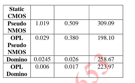
The delay, power dissipation, & energy at output for half adder designed by using different logic families are given in table1 which facilitates the comparison of these logic families.
Table 1: comparison among different logic families used to design half adder
Logic family
Delay in nSec.
Power dissipation
in µW
Maximum energy in
mV Static
CMOS
1.0265 0.018 320.63
OPL 0.5105 0.016 209.10
Static CMOS Pseudo NMOS
1.019 0.509 309.09
OPL Pseudo NMOS
0.029 0.380 198.10
Domino 0.0245 0.026 258.67 OPL
Domino
[image:7.612.331.553.100.236.2]0.006 0.017 223.97
[image:7.612.64.569.106.456.2]Table 1 show that OPL can provide considerable speedups at lower power dissipation for the half adder circuit when OPL is applied to conventional logic families. The comparison among different logics for full adder circuit is shown in table 2.
Table 2: comparison among different logic families used to design full adder
Logic family Delay in nSec.
Power dissipation
in µW
Maximum energy in
mV Static CMOS 0.046 0.028 233.86 OPL Static CMOS 0.0105 0.018 162.71 Pseudo NMOS 0.0315 0.922 222.64
OPL Pseudo NMOS
0.016 0.360 189.72
Domino 0.0265 0.035 253.15 OPL Domino 0.0135 0.024 120.82
When applied to static CMOS the OPL provide speedups upto 2.01x & 4.3x for half adder & full adder circuits, similarly speedups of 4.08x and 1.12x are achieved over the fastest known logic i.e. domino logic for half adder & full adder circuits.
V. CONCLUSION
I N T E R N A T I O N A L J O U R N A L F O R R E S E A R C H I N A P P L I E D S C I E N C E
AN D E N G I N E E R I N G T E C H N O L O G Y (I J R A S E T)
Page 105 ups & reduction in power dissipation are achieved but a slightly increased expense of area consumption.
REFERENCES
[1] Sentamilselvi M, Mahendran P, “High performance adder
circuit in VLSI system”, International journal of
technology enhancements and emerging engineering research, ISSN 2347-4289, Vol. 2, Issue 3, pp. 80-83, 2014.
[2] N. Srinivasa Gupta, M. Satyanarayana, “A novel domino
logic for arithmetic circuits”, International journal of innovative technology and exploring engineering (IJITEE) ISSN: 2278-3075, Volume-3, Issue-3, pp. 34-37, August 2013.
[3] Pakkiraiah Chakali, Adilakshmi Siliveru, Neelima
Koppala, “Design of high speed six transistor full adder
using a novel two transistor XOR gates” International Journal of Advanced Research in Computer Science and Electronics Engineering Volume 1, Issue 5, ISSN- 2277 – 9043, pp. 104-108, July 2012.
[4] M.B. Damle, Dr. S. S. Limaye, “64 bit domino logic adder with 180nm CMOS technology” International Journal of Advanced Research in Computer Engineering & Technology Volume 1, Issue 4, ISSN- 2278 – 1323, pp. 1-5, June 2012.
[5] Chiranjeevi Pandamaneni, Mr.Syed Inthiyaz, Aditya.K,
B.V.Aravind, “Implementation of low power high
performance combinational circuits using output
prediction logic” International Journal of Engineering
Research and Applications (IJERA), ISSN: 2248-9622 Vol. 2, Issue 2, pp.1316-1321, Mar-Apr 2012.
[6] Neil H.E.Weste, David Harris, Ayan Banerjee “CMOS VLSI design-a system perspective”, Pearson publication, 3rd edition, ISBN 978-81-7758-568-1, pp.216-229, 2012. [7] Sheng Sun, Larry McMurchie and Carl Sechen, “A high
-performance 64-bit adder implemented in output
prediction logic” IEEE, ISSN 1522-869X, pp. 213-222, 2001.
[8] Larry McMurchie, Su Kio, Gin Yee, Tyler Thorp, and
Carl Sechen, “Output prediction logic: a high
![Figure 2: OPL predicting ones [7]](https://thumb-us.123doks.com/thumbv2/123dok_us/8587825.862950/3.612.340.531.148.235/figure-opl-predicting-ones.webp)