Technology (IJRASET)
Design and Simulation of Sixth order parallel
coupled line band pass Chebyshev filter
Shikha Swaroop Sharma1, Swati Sharma2
1
Department of Electronics and Communication Engineering, Birla Institute of Technology, Mesra, Ranchi-835215, India 2
Department of Electronics and Communication Engineering, SRM University –Delhi NCR Campus, Ghaziabad, U.P., India
Abstract: The aim of this paper is to simulate sixth order 16.5 Ghz parallel coupled line Chebyshev band pass filter with 0.1db ripple. Simple simulation study and calculation are presented with RT duroid 5880 substrate. Element values determination formulas are expressed in terms of microstrip line impedances. To study the simulation ADS software is used and both forward transmission |S11| and reflection coefficient |S21| are represented. The result shows that filter works well at operating frequency.
Keywords Band passes filter, Chebyshev, parallel coupled line.
I. INTRODUCTION
A filter is a frequency selective two port network which passes the desired frequency from a group of frequencies. Filter is an important component in RF and microwave application. Nonlinear circuits such as mixers and amplifier usually generate unwanted frequency components such as image signals, distortion etc. these signal degrade the system performance.
In recent communication there is a need for high performance, small size, light weight and low cost band pass filter. Parallel coupled microstrip line filter are widely used in RF front end of both microwave and wireless communication. This paper focuses on the performance of parallel coupled line microstrip band pass asymmetrical filter of quarter wavelength transmission line.
A. Filter Design
In this paper the filter is designed using Chebyshev low pass prototype. The element values for 0.1db ripple are taken from [1-5] after that these values are assigned to LC elements. Based on the desired attenuation i.e. 40db the value of n is selected which determines the order of filter.
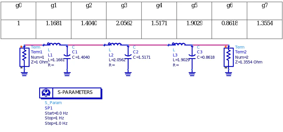
g0 g1 g2 g3 g4 g5 g6 g7 1 1.1681 1.4040 2.0562 1.5171 1.9029 0.8618 1.3554
C
C2 C=1.5171
S_Param
S-PARAMETERS
L
L1
R= L=1.1681
Term
Term2
Z=1.3554 Ohm Num=2
C
C3 C=0.8618
L
L3
R= L=1.9029
L
L2
R= L=2.0562
C
C1 C=1.4040
Term
Term1
[image:2.612.64.548.446.672.2]Technology (IJRASET)
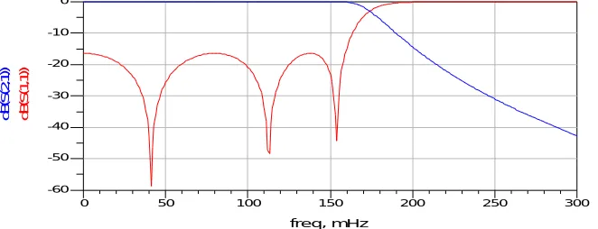
Fig 2: Simulated S21 and S11 of Low Pass Prototype
The next step is to find the lumped element values of LC section of band pass filter using frequency and impedance scaling. The frequency is scaled to the desired mid band frequency of 16.5Ghz and the source impedance is scaled to 50Ω.
Ls=
c
gi
W
where
c
=cutoff frequency
W
=bandwidth
=50 Ω
gi
=corresponding element valueCs=
2
1
s
L
where 2
=2Πf1*2Πf2Similarly,
Cp=
c
gi
W*
and
Lp=
1
2p
C
After scaling the circuit diagram along with response is shown
50 100 150 200 250
0 300
-50 -40 -30 -20 -10
-60 0
freq, mHz
d
B
(S
(1
,1
))
d
B
(S
(2
,1
Technology (IJRASET)
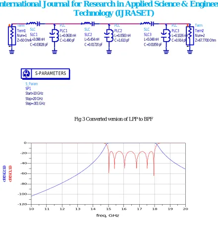
Fig 3 Converted version of LPP to BPF
Fig 4 Simulated lossless response of Band pass filter
Since, at high frequency the dimension of the device becomes comparable to the wavelength of operation so there is a need to convert lumped circuit diagram into microstrip transmission line structure. To convert the circuit into corresponding transmission lines the even and odd impedances are determined using the admittance inverters. The design equations for this type of filter are given by
1
FBW
2 g g
o
J
Y
S_ParamSP1
Step=.001 GHz Stop=20 GHz Start=10 GHz
S-PARAMETERS Term
Term1
Z=50 Ohm Num=1
Term
Term2
Z=67.7700 Ohm Num=2 PLC
PLC3
C=0.914 pF L=0.1026 nH SLC
SLC3
C=0.01859 pF L=5.048 nH PLC
PLC2
C=1.610 pF L=0.0583 nH SLC
SLC2
C=0.01720 pF L=5.454 nH PLC
PLC1
C=1.490 pF L=0.0630 nH SLC
SLC1
C=0.03028 pF L=3.098 nH
11 12 13 14 15 16 17 18 19
10 20
-100 -80 -60 -40 -20
-120 0
freq, GHz
d
B
(S
(1
,1
))
d
B
(S
(2
,1
Technology (IJRASET)
, 1n n+1
FBW
2 g g
n n
o
J
Y
where g0, g1… gn are the element of a ladder-type low-pass prototype with a Normalized cutoff Ωc = 1, and FBW is the fractional bandwidth of band-pass filter. J j, j+1 are the characteristic admittances of J-inverters and Y0 is the characteristic admittance of the terminating lines.
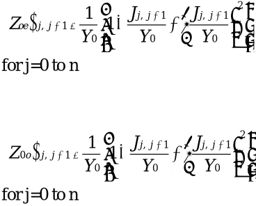
To realize the J-inverters obtained above, the even- and odd-mode characteristic impedances of the coupled microstrip line resonators are determined by
2
, 1 , 1
, 1
0 0 0
1
1
for j=0 to n
j j j j oe j j
J
J
Z
Y
Y
Y
2
, 1 , 1
0 , 1
0 0 0
1
1
for j=0 to n
j j j j
o j j
J
J
Z
Y
Y
Y
[image:5.612.113.297.203.351.2]Using above design equations yield the design parameters, which are tabulated as follows: Table 1
S.No W(width) L(length) S(height) 1 3.011440 1.871460 0.049951 2 3.960950 1.839140 0.495784 3 4.144790 1.832760 0.874624 4 4.161480 1.832200 0.933172 5 4.144790 1.832760 0.874624 6 3.960950 1.839140 0.495784 7 3.011440 1.871460 0.049951
The dimensions of the parallel line for the filter are determined using the line calc tool in ADS also verified by equations. The correction factor of 0.165b, where b is the ground plane spacing is subtracted from the basic length L of quarter wavelength.
II. RESULT AND CONCLUSION
Technology (IJRASET)
REFERENCES Term Term1 Z=50 Ohm Num=1 Term Term2 Z=50 Ohm Num=2 Goal OptimGoal1 RangeMax[1]=18GHz RangeMin[1]=15GHz RangeVar[1]="freq" Weight=1 Max=-40 Mi n=-20 Si mInstanceName="SP1" Expr="dB(s (1,1))" GOAL S_Param SP1 Step=0.0001 GHz Stop=25.0 GHz Start=10.0 GHz S-PARAMETERS MSUB MSub1 Rough=0 mil T anD=0.0009 T =0 mil Hu=1.57 mm Cond=5.88E+7 Mur=1 Er=2.2 H=1.57 mm MSub MCFIL CLin1L=2.994336 mm {t} {o} S=0.049951 mm {t} {o} W=2.409152 mm {t} {o} Subs t="MSub1" MCFIL
CLin2
L=2.75871 mm {t} {o} S=0.495784 mm {t} {o} W=3.16876 mm {t} {o} Subst="MSub1"
MCFIL
CLi n7
L=2.80719 mm {t} {o} S=0.049951 mm {t} {o} W=2.10844 mm {t} {o} Subst="MSub1" MCFIL
CLin3
L=2.74914 mm {t} {o} S=0.874624 mm {t} {o} W=3.315832 mm {t} {o} Subs t="MSub1"MCFIL
CLin4
L=2.7483 mm {t} {o} S=0.933172 mm {t} {o} W=3.329184 mm {t} {o} Subs t="MSub1"MCFIL
CLin5
L=2.74914 mm {t} {o} S=0.874624 mm {t} {o} W=2.901353 mm {t} {o} Subs t="MSub1" MCFIL
CLin6
L=2.75871 mm {t} {o} S=0.495784 mm {t} {o} W=2.772665 mm {t} Subs t="MSub1" m 1 f req= dB(S(1, 1))=-15.537 15.74GHz m 3 f req= dB(S(1, 1))=-15.781 Peak 17.30GH z m2 f req= dB(S(1,1))=-43.654 Valley 16.15GHz
11 12 13 14 15 16 17 18 19 20 21 22 23 24
10 25 -100 -95 -90 -85 -80 -75 -70 -65 -60 -55 -50 -45 -40 -35 -30 -25 -20 -15 -10 -5 -105 0
freq , GHz