International Journal of Emerging Technology and Advanced Engineering
Website: www.ijetae.com (ISSN 2250-2459,ISO 9001:2008 Certified Journal, Volume 4, Issue 5, May 2014)
242
AC Link Inverter Based on Multiple Carrier PWM For Fuel
Cell
Deepa Zamwar
1, Jitendra Singh Bhadoriya
21M.Tech Final Year Student, 2Assistant Prof., NRI Institute of Information Science & Technology, RGPV University, Bhopal ,
India
Abstract— The paper suggests the development of a low
cost fuel cell inverter system. The approach consists of a three-terminal push-pull inverter to boost the fuel cell voltage of 24V to ±220V ac with HF transformer (1KHz frequency). High-frequency ac link conversion offers a possible way to reduce the number of power stages, in the form of a
cycloconverter. The approach keeps the number of stages
and magnetic elements low while providing galvanic isolation. Either SCRs or IGBTs can be used as output devices, which provide an unusual cost/performance trade-off possibility. Gate drives and other control elements are also simplified. The design provides excellent performance with a minimum filter components and a simple control.
Keywords— Cycloconverter, Inverter, Simulation,
Multivibrator, Fuelcell
I. INTRODUCTION
For the power conversion system where linkage with ac system line is required, the HF (high-frequency) link converter topology has been attracting special interests recently, because it enables the power converters to be compact and light-weight. Two types are considered in the high frequency converters. One is a dc/dc converter type and other is a cycloconverter (ac/ac) type.
This paper details the application of low cost fuel cell inverter using multiple carrier PWM for ac-ac converter. The power conversion is more direct (two stages).Also
PWM cycloconverter, with or without natural
commutation, and conventional PWM inverter is unified through a multiple carrier PWM framework. Issues about complexities are resolved. Multiple carrier PWM methods lead HF link inverters that are about as simple as conventional PWM inverter.
The visions of a fuel cells potential are diverse. They include fuel cells powering cars, operating as backup or even primary power for your home from a shed-sized fuel-cell system, and providing power for larger commercial buildings and computer installations. Such systems can produce significant power. Though practical model is build but with some minor modifications commercial fuel cell inverter can be built.
II. OVERVIEW OF SCHEME
Fig.1 shows block diagram for the scheme. Input is 24V battery/fuel cell with capacitor for filter. Inverter is of push pull configuration with 1KHZ frequency. Cycloconverter is having 50Hz frequency. Isolation is obtained from high frequency transformer.
dc Input Inverter Isolation Cyclo
converter Load
Control Circuit Control
Circuit
Fig.1 Block Diagram
i. Control Block for Inverter
Gate pulses are applied to switches of push pull inverter. Phase delay is introduced between pulses as Shown in Fig 2. Gate pulses are in synchronization with 2 KHz ramp.
Delay Circuit 1
Delay Circuit 2
Gate 1
Gate 2 Synchronized
Control pulse
Square Wave Output Inverter
Fig.2 Control Block for Inverter
ii.Control Block for Cycloconverter
International Journal of Emerging Technology and Advanced Engineering
Website: www.ijetae.com (ISSN 2250-2459,ISO 9001:2008 Certified Journal, Volume 4, Issue 5, May 2014)
243
Ramp Generator
Sine Wave Generator
Phase Shift Comparator 1
Comparator 2 Delay
Delay
Phase delayed Pulse
Phase Advanced Pulse
Gate Pulse For Positive Converter
Gate Pulse For Negative Converter
Driver
Driver
Cycloconverter 2KHz
50Hz
1800
Load Current Sensor
Logic Unit
Fig.3 Control Block for Cyclconverter
As shown in Fig.3 control module contains ramp generator of frequency 2KHz which also gives square wave of 1KHz to be applied as control for forward converter i.e. inverter.
Sine wave obtained at 50Hz is modulating signal. For multiple carrier operation this sinusoidal waveform is phase shifted by 1800.
By comparing carrier and modulating signal PWM output is obtained. This PWM output is advanced or delayed for achieving phase advanced and phase delayed trigger pulses respectively. Such pulse train is obtained using multivibrator (delay block in Fig.3).
The delayed waveform is blanked when the current is negative, while the advanced waveform is blanked when the current is positive.
The two multivibrators are triggered from the rising edge of the respective comparator to produce a 15μs gate pulse train. The upper multivibrator creates a phase-delayed gate pulse train to be used when load current is positive, while the lower multivibrator creates a phase-advanced gate pulse train to be used when the load current is negative. Simple logic is used with a current comparator to separate the positive and negative current conditions.
These trigger pulses are combined with another input obtained from current polarity detector. This current polarity detector detects current direction across load.
Thus trigger pulses obtained are applied to positive and negative converter of cycloconverter through driver.
iii. Power Block
Power block is described under two sections, as this consists of primary side and secondary side with isolation as shown in Fig.3.
The primary side, inverter operation is obtained through push-pull configuration while output is single phase bridge consisting of 8 SCRs connected in antiparallel. RC snubber is designed for switches.
iv. Inverter
As shown in Fig.4, inverter consists of push pull inverter which converters 24V dc to 96Vp-p, 1 KHz square wave. This push pull inverter uses two MOSFETs as switches. Driver for MOSFET is obtained by transistorized circuit. Driver signals are synchronized with 2 KHz ramp. Inverter switches at 1KHz. Filtering of dc voltage from battery is done through capacitor.
dc Battery Push Pull Inverter
Synchronized Gating Signals
Square Wave
24V 96Vp-p, 1 KHz
Fig.4 Inverter
v. Cycloconverter
Fig.5 shows schematic for ac-ac converter along with current polarity detection. Commutation of cycloconverter during the zero crossing of load current is an important control issue, well understood from conventional ac cycloconverter results. Ideally, the current polarity detection scheme in Fig.5 would use the “fundamental current zero”. While this scheme results in ideal commutation with no cross-over distortion, it is known to be difficult to implement in practice. Instead, Fig.5 uses a modification to the “first current zero”
ac-ac Converter R-L Load
Current Polarity Detection
International Journal of Emerging Technology and Advanced Engineering
Website: www.ijetae.com (ISSN 2250-2459,ISO 9001:2008 Certified Journal, Volume 4, Issue 5, May 2014)
244
As shown in block diagram secondary of power module consists of single phase ac-ac converter with 8 SCRs along with 4 RC snubbers. Load connected is RL and switching is controlled from trigger pulses obtained from control module whose feedback is from current polarity detector, which senses the load fed from cycloconverter. Isolation between source and load is obtained using HF transformer. This transformer uses ferrite core to achieve high frequency square wave transfer.
III. DESIGN OF INVERTER CONTROL BLOCK
Synchronized square pulse is obtained which is phase shifted and delayed before applying to switches.
i. Design of Synchronized Square Pulse
Synchronized square pulse is achieved from ramp generator as shown in Fig.6. D flip flop IC4013 is used with reset on ON facility. Clock is given through non-inverting buffer consisting of CE amplifier with BC 546. Diode IN4148 is used as edge detector and for bypassing negative cycle.
IC4013 is used to generate square wave of 1 KHz synchronized with 2 KHz ramp. Clock frequency is also 2 KHz. The CD4013B dual D-type flip-flop is used.
Q Q
SET CLR
D From Ramp
Generator
10kΩ 10kΩ
10kΩ 10kΩ
10kΩ 10kΩ
4148
+12V
1KHz Square Pulse
+12V +12V
4148 .1μF
Fig.6 Synchronized Square Pulse
ii.Design of Gate Pulse
The 50% duty cycle for gate pulses still support pulse transformer coupling, retaining the simplicity of the gate drive isolation. The PWM cycloconverter process scales directly to higher switching speeds possible with these devices. NAND gate IC 4093 is used for inversion in gate pulse. Delay is obtained using standard RC circuit.
R = 10 K Ω C = 0.01 μF R*C = 0.1ms
1KHz Square Pulse
10KΩ
10KΩ
.01μF .01μF IC4093
Fig.7 Gate Pulses for Inverter
iii. Design of RampGenerator
Ramp Generator is achieved from triangular wave generator by inserting a variable dc voltage into the non-inverting terminal of the integrator A2 as shown in Fig.6. A duty cycle less than 50% causes output of A2 to be a ramp. When R4 wiper is moved toward –VEE, the rise time of ramp becomes longer than fall time. Also frequency of ramp is adjusted with R4. Amplitude of output is independent of R4.
Design is done for 7Vp-p, 2 KHz positive going ramp using op-amp [13]
fo = 2 KHz
R2/ R3 = Vp-p / 2*Vsat Let Vp-p = 7V
R2 = 10 KHz Vsat = 12V R3 = 34.28 KΩ
Choose R3 = 22K+10Kpot fo = R3/4 R1*C1*R2 R1*C1 = 0.4ms Let C1 = 0.47μF R1 = 851 Ω Let R1 = 1KΩ
Where fo ---Output frequency in Hz. Vp-p--- peak to peak output voltage
International Journal of Emerging Technology and Advanced Engineering
Website: www.ijetae.com (ISSN 2250-2459,ISO 9001:2008 Certified Journal, Volume 4, Issue 5, May 2014)
[image:4.612.57.286.139.271.2]245 0.47μF 1KΩ +12V -12V 2.2KΩ 2.2KΩ 20KΩ 10KΩ 22KΩ 10KΩ 6KΩ 1KΩ 47KΩ +12V -12V 6.2V 6.2V -+ -+ + -10KΩ Ramp Output To Inverter Control Block A1 A2 A3 LM 348
Fig.8 Ramp Generator
a. Design of Sine Wave Generator
Sine wave is obtained using bridge oscillator [13] as shown in Fig.9. Designing is
done at 12Vp-p, 50 Hz frequency. fo = 0.159/Rc
R*C =3.18ms Let C = 0.47 μF R = 6.7 KΩ Gain Rf ‘[/ R1 = 2 Let R1=5.'1 KΩ R1=5.1 KΩ Rf = 10 KΩ Rf = 10 KΩ pot
[image:4.612.351.548.145.251.2]2 Vp-p is achieved using potential divider as shown in Fig. 9. Buffer is also connected. This sine wave is further inverted using op-amp as inverting amplifier. Gain for this op-amp is set as 1 with combination of 10 K and 9.1 K and 2K pot. 0.47μF 1KΩ 1KΩ 6KΩ 6 .8 K Ω 10KΩ 5.1KΩ 10KΩ 10KΩ +12V +12V + -+ -+ Sine Output LM 324 0 .4 7 μ F 9.1KΩ 2KΩ 6.8KΩ + -A B C D TO Comparator 1 TO Comparator 2
Fig. 9
b. Design of Comparator
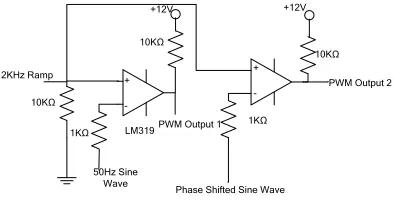
For obtaining PWM comparison is done between ramp and sine using high speed voltage comparator dual comparator LM319. Modulation index is set to 0.66.
+12V 1KΩ 10KΩ 1KΩ -+ -+ 10KΩ 10KΩ +12V LM319 2KHz Ramp
Phase Shifted Sine Wave 50Hz Sine
Wave
PWM Output 2
PWM Output 1
Fig.10 PWM Generator
c. Design of Multivibrator
[image:4.612.384.508.344.470.2]The MC14538B is a dual, retriggerable, resettable monostable multivibrator. It may be triggered from either edge of an input pulse, and produces an accurate output pulse over a wide range of widths, the duration and accuracy. 1.5KΩ 0.01μF 1.5KΩ 0.01μF 10KΩ 0.1μF 12V 12V 12V 12V PWM Input 1 PWM Input 2 Delay Output 1 Delay Output 2 IC 4538
Fig.11 Delay Output
of which are determined by the external timing components, CX and RX.
For 15μs delay value of CX and RX are chosen as 0.01μF and 1.5KΩ respectively.
d.Design of Logical Unit
Design for Delayed and Advanced circuit- NOR
(IC4001) logic is used for obtaining phase advanced and phase delayed trigger pulses.
[image:4.612.52.278.507.632.2]Phase Delayed Pulses Phase Advanced Pulses Current Feedback 10KΩ + -12V LM311 MC14001 PWM Input PWM Input
[image:4.612.353.501.612.681.2]International Journal of Emerging Technology and Advanced Engineering
Website: www.ijetae.com (ISSN 2250-2459,ISO 9001:2008 Certified Journal, Volume 4, Issue 5, May 2014)
246
Design for Feedback Network - Single comparator is
required for comparing feedback current obtained from load and PWM output obtained. Input is connected in differential mode as shown in Fig.12.
Both the inputs and the outputs of the LM311 can be isolated from system ground, and the output can drive loads referred to ground, the positive supply or the negative supply.
e. Design of Driver
The driver circuit of cycloconverter consists of Pulse Transformer and transistors along with diode and resistances. As cycloconverter is having SCRs as switches only edges are required for trigger. To obtain voltage level transistor is used as an amplifier. Standard configuration is applied for achieving trigger pulses as shown in Fig.13. Transistor BD139 is used as driver and BC546 as buffer. Such unit is used for each SCR.
1kΩ
10kΩ
1kΩ 1kΩ
10kΩ
1kΩ 100Ω 4007
4007 PT
BD139 BC546
12V
12V
Trigger Pulse
Trigger to SCR
Fig.13 Driver of SCR
IV. POWER CIRCUIT DESIGN
i. Design of Inverter
Inverter is designed using push pull configurations and calculations are done as per requirement. Gate pulse is obtained from circuit shown in previous chapter. MOSFET is chosen for high frequency switching. Two 12V batteries are connected in series for obtaining 24V as fuel cell is not available. Batteries used are of standard company with 1A-Hr rating.
ii.Design of Push Pull Inverter
24 Vdc is converted into square wave of 1 KHz frequency and amplitude of 48V at primary of output transformer using push-pull inverter. This is achieved by circuit shown in Fig.14.
Care is taken that switch has low saturation voltage and breakdown voltage is two to three times the supply voltage. Isolation is obtained through HF transformer which is described in the next section. Capacitor value 220μF/63V is connected across 24V battery for filtering.
Edc = 24V Eout = 220V Po = 200W Io = 1A Let η = 70% Pin = 285W Iin = Pin/Edc =6A
24V
220μF/63V
47kΩ 47kΩ Gate Pulse
Gate Pulse
HF Transformer 1:2
200V Square Wave
Fig.14 Push Pull Inverter
IRF540N Power MOSFET is used.
iii. Design of MOSFET Snubber
fs = 1KHz Edc = 24V iL=6A Let L = 25 μH tf = 40x10-9 s where
tf is fall time
fs switching frequency C = iL*tf / Edc = 6 * tf / 24 C = 0.01μF L = Edc*tr / iL tr = 6.25 μs
where tr is rise time di/dt = iL/tr
= 0.96A/μs Switch ON di/dt = 0.24 A/μs R = √(4*L/C) R = 100 Ω
International Journal of Emerging Technology and Advanced Engineering
Website: www.ijetae.com (ISSN 2250-2459,ISO 9001:2008 Certified Journal, Volume 4, Issue 5, May 2014)
247
iv. Design of Transformer
Ferrite core is used for transformer as operation frequency is 1KHz and input is Square Wave. Core is selected as per power requirement.
Edc = 24V Eout = 220V Po = 200W Io = 1A Let η = 70% Pin = 285W Iin = Pin/Edc = 6A
As per calculations core required was EE-65x33x28 but due to its non-availability core used is EE-55x27x21 type 5s
Area = 20mmx17mm N = Eout/Edc = 5
Eout ×105 Ns = --- 4×Bmax×A×f Bmax = 4800G Br = 1800G Hc = 11.9A/m Let Bmax = 3150G
Calculating from above equation Ns = 462
Np = 93
As push pull type hence each primary winding will have 93 turns each.
Maximum current rating is reduced due to core used.
v. Design of ac-ac Converter
Secondary of high frequency transformer drives bridge of SCRs connected in anti-parallel and bridge is working as cycloconverter. SCRs are triggered from pulse transformer.
vi. Design of Cycloconverter
As explained in a previous section current is approximately 1A hence SCR rating is chosen accordingly. As shown in Fig.15 eight SCRs are connected in anti-parallel to achieve ac-ac converter configuration. T1-T4 comprise of positive converter while T5-T8 comprise of negative converter.
SCR used is TYN612 having following features:
IT(RMS) -RMS on-state current (180° conduction angle) is 12 A
VDRM/VRRM Repetitive peak off-state forward voltage is 600 to 1000 V
IGT Gate Current is 0. 2 to 15 mA
T1
200mH 26Ω CT T3
T2 T4
T5
T6
T8
T7 Load
Fig.15 Cycloconverter
Load is inductive load of 200 mH with self resistance of value 26 Ω.
Current transformer is connected to obtain current polarity for feedback. Construction of current transformer is done to achieve ratio of 1:300.
N1I1 = N2I2 2x1A = 600xI2 I2 = 3mA V = IR
= 3x10-3 x 220 Ω, = 660mV
Secondary of current transformer is connected with resistance R(220Ω) whose value is chosen such that voltage obtained across R is enough as input to comparator LM311 connected in triggering circuit for selection of positive and negative converter.
vii. Design of Thyristor Snubber
Let dv/dt = 400 V/μs L = 25 μH
dv/dt = E*R/L E = 100V
Where E is secondary voltage peak. R = 100 Ω
International Journal of Emerging Technology and Advanced Engineering
Website: www.ijetae.com (ISSN 2250-2459,ISO 9001:2008 Certified Journal, Volume 4, Issue 5, May 2014)
248
Hence value for snubber chosen is 100 Ω ,1W and 0.01μF/250V.
For heat sink PHS-16 is used as power dissipation is very low.
V. SIMULATION &RESULTS
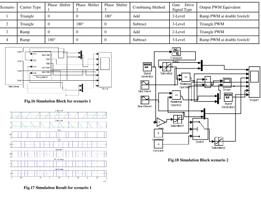
Simulations are done to obtain different gate pulses for different combinations described in table These gate pulses are combined with square wave as HF link voltage to obtain output voltage. (Refer Table 1)
Table 1
Scenario Carrier Type Phase Shifter 1
Phase Shifter 2
Phase Shifter
3 Combining Method
Gate Drive
Signal Type Output PWM Equivalent
1 Triangle 0 0 180° Add 2-Level Ramp PWM at double fswitch'
2 Triangle 0 180° 0 Subtract 3-Level Triangle PWM
3 Ramp 0 0 0 Add 2-Level Triangle PWM
4 Ramp 180° 0 0 Subtract 3-Level Ramp PWM at double fswitch'
[image:7.612.55.567.223.632.2]Fig.16 Simulation Block for scenario 1
Fig.17 Simulation Result for scenario 1
International Journal of Emerging Technology and Advanced Engineering
Website: www.ijetae.com (ISSN 2250-2459,ISO 9001:2008 Certified Journal, Volume 4, Issue 5, May 2014)
249 Fig.19 Simulation Result for scenario 2
Transport Delay
Switch Sine Wave1
Sine Wave
Signal Generator1 Signal
Generator
Scope1
Saturation2 Saturation1 Saturation
>=
Relational Operator1
>=
Relational Operator
OR
Logical Operator -1
Gain1 -1
Gain
5
Constant1
-5
Constant
Fig.20 Simulation Block for scenario 3
Fig.21 Simulation Result for scenario 3
Transport Delay
Switch Sine Wave
Signal Generator1 Signal
Generator
Scope1
Saturation2 Saturation1
Saturation >=
Relational Operator1
>=
Relational Operator
5
Constant1
-5
Constant
Fig.22 Simulation Block for scenario 4
International Journal of Emerging Technology and Advanced Engineering
Website: www.ijetae.com (ISSN 2250-2459,ISO 9001:2008 Certified Journal, Volume 4, Issue 5, May 2014)
250
VI. CONCLUSION
The scheme suggested shows that the number of stages can be reduced, leading to a HF-link conversion approach. The reduction came from recognizing redundancy in the power processing. Without a dc link bus, rectifiers and filter components along with their associated losses are eliminated. Applying the techniques of multiple carrier PWM cycloconversion results are exactly identical to conventional PWM techniques.
The combination of a current-controlled input, adjust the average power demand from a fuel cell, battery buffer, and PWM cycloconverter, provides a reduced parts-count solution compared to conventional boost-forward-inverter cascade topology. The combined converter isolates the fuel cell from its load both electrically and dynamically while reducing parts count and therefore reduces costs.
REFRENCES
[1] M. Koyama, “High frequency link dc/ac converter with PWM cycloconverter for UPS,” in Proc. IPEC’90 Conf., Tokyo, Japan, 1990, pp. 748–754.
[2] T. Kawabata, K. Honjo, N. Sashida, K. Sanada, and M. Koyama, “High frequency link dc/ac converter with PWM cycloconverter,”in Proc. IEEE Industry Applications Soc. Annu. Meeting, 1990, pp. 1119–1124.
[3] T. Aoki, K. Yotsumoto, S. Muroyama, and Y. Kenmochi, “A new uninterruptible power supply with a bidirectional cycloconverter,” in Proc. IEEE Int. Telecommunications Energy Conf., 1990, pp. 424– 429.
[4] J. Kassakian, M. Schlecht, and G. Verghese, Principles of Power Electronics. Reading, MA: Addison-Wesley, 1991, pp. 186–187. [5] N. H. Kutkut, D. M. Divan, D. W. Novotny, “Charge equalization of
series connected battery strings,” IEEE Trans. Industry Applications, vol. 31, no. 3, pp. 562-568, May 1994.
[6] R. D. Brost, “Performance of valve-regulated lead-acid batteries in EV1 extended series strings,” in Proc. 13th Annual Battery Conf. On Applications and Advances, 1998, pp. 25-29.
[7] S. West and P. T. Krein, “Equalization of valve-regulated lead-acid batteries: issues and life test results,” in Proc. IEEE Int. Telecommunications Energy Conf., 2000, pp. 439–446.
[8] S. West, P. T. Krein, "Equalization of valve-regulated lead-acid batteries: issues and life test results," in Proc. IEEE Int'l Telecommunications Energy Conf., 2000, pp. 439-446. [9] P. T. Krein, “Tricks of the Trade: Simple Solar Cell Models,” IEEE
Power Electronics Society Newsletter, April 2001. [10] Fuel cells, IEEE Spectrum. June 2001.
[11] S. Haykin, Communication Systems, 4th ed. New York: Wiley, 2001, p. 211
[12] B. R. Pelly, Thyrister Phase Controlled Converters and Cycloconverters. New York: Wiley-Interscience, 1971.
[13] Op-Amps and Linear Integrated Circuits by Ramamkant A.Gayakwad
Authors Profile
Deepa Zamwar is a research scholar, Pursuing her M.Tech., at NRI Institute of Information Science and Technology, RGPV University, Bhopal , India.
Guided By
Jitendra Singh Bhadoriya