International Journal of Emerging Technology and Advanced Engineering
Website: www.ijetae.com (ISSN 2250-2459,ISO 9001:2008 Certified Journal, Volume 3, Issue 12, December 2013)
362
FPGA Implementation of Low-Area Floating Point
Multiplier Using Vedic Mathematics
R. Sai Siva Teja
1, A. Madhusudhan
21
M.Tech Student, 2Assistant Professor, Dept of ECE, Anurag Group of Institutions (formerly CVSR College of Engineering), Ghatkesar, R. R Dist, A.P, India
Abstract—In this paper we describe an efficient implementationof an IEEE 754 single precision floating point multiplier using vedic mathematics .The purpose of using vedic mathematics is due to increase in the number of partial products in normal multiplication process ,with using vedic mathematics partial products can be reduced so that the area and power constraints of the floating point multiplier can be reduced efficiently.
Keywords-- floatingpoint; multiplication, FPGA, Nikhilamsutra, Radix selection unit, Vedic mathematics.
I. INTRODUCTION
Floating point numbers are one possible way of representing real numbers in binary format; the IEEE 754 [1] standard presents two different floating point formats, Binary interchange format and Decimal interchange format. Multiplying floating point numbers is a critical requirement for DSP applications involving large dynamic range. This paper focuses only on single precision normalized binary interchange format. Fig. 1 shows the IEEE 754 single precision binary format representation; it consists of a one bit sign (S), an eight bit exponent (E), and a twenty three bit fraction (M or Mantissa). An extra bit is added to the fraction to form what is called the significand1. If the exponent is greater than 0 and smaller than 255, and there is 1 in the MSB of the significand then the number is said to be a normalized number; in this case the real number is represented by (1)
Figure1. IEEE single precision floating point format
Z = (-1S) * 2 (E -Bias) * (1.M)
Where M = m22 2 -1
+ m21 2 -2
+ m20 2
-3+…+ m1
2-22+ m0 2-23;
Bias = 127.
Multiplying two numbers in floating point format is done by 1- adding the exponent of the two numbers then subtracting the bias from their result, 2- multiplying the significand of the two numbers, and 3- calculating the sign by XORing the sign of the two numbers. In order to represent the multiplication result as a normalized number there should be 1 in the MSB of the result (leading one).
Floating-point implementation on FPGAs has been the interest of many researchers. In [2], an IEEE 754 single precision pipelined floating point multiplier was implemented on multiple FPGAs (4 Actel A1280). In [3], a custom 16/18 bit three stage pipelined floating point multiplier that doesn‟t support rounding modes was implemented. In [4], a single precision floating point multiplier that doesn‟t support rounding modes was implemented using a digit-serial multiplier: using the Altera FLEX 8000 it achieved 2.3 MFlops. In [5], a parameterizable floating point multiplier was implemented using the software-like language Handel-C, using the Xilinx XCV1000 FPGA; a five stages pipelined multiplier achieved 28MFlops. In [6], a latency optimized floating point unit using the primitives of Xilinx Virtex II FPGA was implemented with a latency of 4 clock cycles. The multiplier reached a maximum clock frequency of 100 MHz.
II.FLOATING POINT MULTIPLICATION ALGORITHM
As stated in the introduction, normalized floating point numbers have the form of Z= (-1S) * 2 (E -Bias) * (1.M). To multiply two floating point numbers the following is done:
1. Multiplying the significand; i.e. (1.M1*1.M2) 2. Placing the decimal point in the result 3. Adding the exponents; i.e. (E1 + E2 – Bias) 4. Obtaining the sign; i.e. s1 xor s2
International Journal of Emerging Technology and Advanced Engineering
Website: www.ijetae.com (ISSN 2250-2459,ISO 9001:2008 Certified Journal, Volume 3, Issue 12, December 2013)
363
6. Rounding the result to fit in the available bits 7. Checking for underflow/overflow occurrence 1
Significand is the mantissa with an extra MSB bit. This research has been supported by Mentor Graphics. Consider a floating point representation similar to the IEEE 754 single precision floating point format, but with a reduced number of mantissa bits (only 4) while still retaining the hidden „1‟ bit for normalized numbers:
A = 0 10000100 0100 = 40, B = 1 10000001 1110 = -7.5
To multiply A and B
1. Multiply significand: 1.0100 × 1.1110 00000 10100 10100 10100 _10100___ _
1001011000 2. Place the decimal point: 10.01011000
3. Add exponents: 10000100
+
10000001
10000010
1
The exponent representing the two numbers is already shifted/biased by the bias value (127) and is not the true exponent; i.e. EA = EA-true + bias and EB = EB-true + bias
And
EA + EB = EA-true + EB-true + 2 bias
So we should subtract the bias from the resultant exponent otherwise the bias will be added twice.
100000101
- 01111111
10000110
4. Obtain the sign bit and put the result together:
1 10000110 10.01011000
5. Normalize the result so that there is a 1 just before the radix point (decimal point). Moving the radix point one place to the left increments the exponent by 1; moving one place to the right decrements the exponent by 1.
1 10000110 10.01011000 (before normalizing)
1 10000111 1.001011000 (normalized)
The result is (without the hidden bit):
1 10000111 00101100
6. The mantissa bits are more than 4 bits (mantissa available bits); rounding is needed. If we applied the truncation rounding mode then the stored value is:
1 10000111 0010.
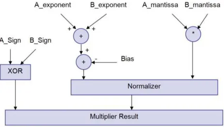
[image:2.612.328.559.409.540.2]In this paper we present a floating point multiplier in which rounding support isn‟t implemented. Rounding support can be added as a separate unit that can be accessed by the multiplier or by a floating point adder, thus accommodating for more precision if the multiplier is connected directly to an adder in a MAC unit. Fig. 2 shows the multiplier structure; Exponents addition, Significand multiplication, and Result‟s sign calculation are independent and are done in parallel. The significand multiplication is done on two 24 bit numbers and results in a 48 bit product, which we will call the intermediate product (IP). The IP is represented as (47 downto 0) and the decimal point is located between bits 46 and 45 in the IP. The following sections detail each block of the floating point multiplier.
Figure 2. Floating point multiplier block diagram
III. VEDIC MATHEMATICS
International Journal of Emerging Technology and Advanced Engineering
Website: www.ijetae.com (ISSN 2250-2459,ISO 9001:2008 Certified Journal, Volume 3, Issue 12, December 2013)
364
The gifts of the ancient Indian mathematics in the world history of mathematical science are not well recognized. The contributions of saint and mathematician in the field of number theory, 'Sri Bharati Krsna Thirthaji Maharaja', in the fonn of Vedic Sutras (fonnulas) are significant for calculations. He had explored the mathematical potentials from Vedic primers and showed that the mathematical operations can be carried out mentally to produce fast answers using the Sutras. In this paper we are concentrating on "Nikhilam Navatascaramam Dasatah" fonnulas and other fonnulas are beyond the scope of this paper.
IV. PROPOSED MULTIPLIER ARCHITECTURE
The mathematical expression for the proposed algorithm is shown below. Broadly this algorithm is divided into three parts. (i) Radix Selection Unit (ii) Exponent Determinant (iii) Multiplier.
Consider two n bit numbers X and Y. kl and k2 are the exponent of X and Y respectively. X and Y can be represented as:
X= Zk1 ± Zl (2)
y = Zk2 ± Z2 (3)
For the fast multiplication using Nikhilam sutra the bases of the multiplicand and the multiplier would be same, (here we have considered different base) thus the equation can be rewritten as
Hardware implementation of this mathematics is shown in Fig. The architecture can be decomposed into three main subsections: (i) Radix Selection Unit (RSU) (ii) Exponent Determinant (ED) and (iii) Array Multiplier. The RSU is required to select the proper radices corresponding to the input numbers. If the selected radix is nearer to the given number then the multiplication of the residual parts (Zl xz2) can be easier to compute. The Subtractor blocks are required to extract the residual parts (ZI and Z2). The second subsection(ED) is used to extract the power (kl and k2) of the radix andit is followed by a subtractor to calculate the value of (k1-k2).The third subsection array multiplier [10] is used to calculate the product (Zl xZZ). The output of the subtractor (klk2)and Zz are fed to the shifter block to calculate the value ofZ2 x Zk1-k2.The first adder-subtractor block has been used to calculate the value of X ± Z2 x Zk1 -k2• The output of the first adder- subtractor and the output of the second Exponent Determinant (k2) are fed to the second shifter block to compute the value of Zk2 x (X ± Z2 X Zk1-k2). The output of the multiplier (ZI xz2) and the output of the second shifter (Zk2 x (X ± Z2 x Zk1-k2))are fed to the second adder subtractor block to compute the value of (Zk2 x (X ± Z2 x Zk1-k2)) ± ZlZ2'
Mathematical expression/or RSU
International Journal of Emerging Technology and Advanced Engineering
Website: www.ijetae.com (ISSN 2250-2459,ISO 9001:2008 Certified Journal, Volume 3, Issue 12, December 2013)
365
Fig-Hard ware implementation of Nikhilam SutraThe Block level architecture of RSU is shown in Fig. RSU consists of three main subsections: (i) Exponent Determinant (ED), (ii) Mean Determinant (MD) and (iii) Comparator. 'n' number bit from input X is fed to the ED block. The maximum power of X is extracted at the output which is again fed to shifter and the adder block. The second input to the shifter is the (n+I) bit representation of decimal '1'.If the maximum power of X from the ED unit is (n-I) then the output of the shifter is i"-I). The adder unit is needed to increment the value of the maximum power of X by 'I'. The second shifter is needed to generate the value of 2".Here n is the incremented value taken from the adder block. The Mean Determinant unit is required to compute the mean of (zn-l + Zn). The Comparator compares the actual input with the mean value of (zn-l+ zn). If the input is greater than the mean then 2" is selected as the required radix. If the input is less than the mean then 2"-1 is selected as the radix. The select input to the multiplexer block is taken from the output of the comparator.
Exponent Determinant
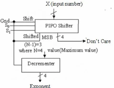
The hardware implementation of the exponent determinant is shown in Fig. 4.The integer part or exponent of the number from the binary fixed point number can be obtained by the maximum power of the radix. For the non- zero input, shifting operation is executed using parallel in parallel out (PIPO) shift registers. The number of select lines (in FigA it is denoted as S], So) of the PIPO shifter is chosen as per the binary representation of the number (N-1)IO. 'Shift' pin is assigned in PIPO shifter to check whether the number is to be shifted or not (to initialize the operation 'Shift' pin is initialized to low). A decrementer [13] has been integrated in this architecture to follow the maximum power of the radix. A sequential searching procedure has been implemented here to search the first 'I' starting from the MSB side by using shifting technique. For an N bit number, the value (N-I)1O is fed to the input of decrementer.
Fig-Hardware implementation of RSU
International Journal of Emerging Technology and Advanced Engineering
Website: www.ijetae.com (ISSN 2250-2459,ISO 9001:2008 Certified Journal, Volume 3, Issue 12, December 2013)
[image:5.612.52.291.149.333.2]366
Fig. Hardware implementation of exponent determinantV. SIMULATION RESULT ANALYSIS
The result analysis is as shown below .Due to the number of partial products have reduced the area is reduced in a fair amount .then no of CLB slices and the flipflops are reduced by a fair amount
The simulation results of the existing and proposed system is as shown below
Specifications Existing system Proposed system
No of slices 604 356
No of Flip Flops 293 108
VI. CONCULSION AND FUTURE WORK
From the above results we can clearly say that the area has been reduced as the utilization of CLB‟s and Flip Flops have been reduced by a fair bit.
The carried out work can be further improved by using highspeed adders and subtsractors.
REFERENCES
[1 ] IEEE 754-2008, IEEE Standard for Floating-Point Arithmetic, 2008. [2 ] B. Fagin and C. Renard, “Field Programmable Gate Arrays and Floating Point Arithmetic,” IEEE Transactions on VLSI, vol. 2, no. 3, pp. 365– 367, 1994.
[3 ] ARadhika pavan kumar UCS Saiprasad Goud A FPGA implementation of highspeed 8-bit vedic multiplier using barrel shifter
[4 ] L. Louca, T. A. Cook, and W. H. Johnson, “Implementation of IEEE Single Precision Floating Point Addition and Multiplication on FPGAs,” Proceedings of 83 the IEEE Symposium on FPGAs for Custom Computing Machines (FCCM‟96), pp. 107–116, 1996. [5 ] A. Jaenicke and W. Luk, "Parameterized Floating-Point Arithmetic
on FPGAs", Proc. of IEEE ICASSP, 2001, vol. 2, pp. 897-900. [6 ] B. Lee and N. Burgess, “Parameterisable Floating-point Operations
on FPGA,” Conference Record of the Thirty-Sixth Asilomar Conference on Signals, Systems, and Computers, 2002
[7 ] “DesignChecker User Guide”, HDL Designer Series 2010.2a, Mentor Graphics, 2010
[8 ] “Precision® Synthesis User‟s Manual”, Precision RTL plus 2010a update 2, Mentor Graphics, 2010.