Design & Analysis of Low power 10T Sram for
High SNM using 45nm Design
Hari Om1, Sharmelle Thangjam2, Vijay Kumar3
1
M.Tech Micro electronics Department, Punjab University Chandigarh
2
Asst Professors, Dept. of ECE Punjab University Chandigarh
3
Asst Professors, Dept. of ECE Punjab University Chandigarh
Abstract: In this paper a new 10T static random access memory cell having decoupled 5T write port with single bitline and single ended read-bitline (RBL) with 5T read port for low power operation. The RBL is precharged upto cell’s supply voltage, and is allowed to charge and discharge according to the stored data bit. A read-enable(RE) signal is used to drive read port inverter, which connects the RBL to the virtual power rails through a transmission gate during the read operation. RBL remains at VDD or increases toward the VDD level for a read-1, and ground or discharges toward the ground level for a read-0. Read-Enable(RE) signal is kept at low level during the write and the hold mode, and connected to high level only during the read operation. The proposed 10T cell in a commercial 45 nm technology provides 420mv read static noise margin, and reduces the write power dissipation by 30.47% and read power dissipation by 23.6% than that of 6T.
Keywords: 10T, low power, precharging, single ended (SE) read bitline (RBL), static random access memory (SRAM), virtual rails, Read Enable.
I. INTRODUCTION
Requirement of fast and low power primary memory for all battery operated device is increasing very rapidly. So we need SRAM’s which are faster and dissipate less power. Hence, power dissipation has become a first class design constraint [1], as static random access memory (SRAM) is the most important digital macro and its portion on a system-on-chip (SoC) is ever increasing [2]. Reducing the SRAM power dissipation will lower the whole system power dissipation and SoC reliability will increase. Supply voltage reduction is one of the straightforward way to reduce the power consumption because reducing supply voltage improves dynamic and leakage power significantly.
Although the six transistor (6T) SRAM cell is mostly used standard in industry, it has many limitations like poor read stability, read static noise margin (RSNM) degradation [3].
In past decades, many efforts have been taken to model a stable SRAM for low power systems. Researchers have presented many configurations for SRAM and adopted different methods which includes negative bitline voltage [5], write back schemes, Dual rail supply power [8], isolating read path from storage node whereas they all have two complementary bitlines which consumes more power during switching.
The SRAM cell single ended (SE) 8T, 9T, 10T and differential 7T , 8T , 9T and 10T eliminates the stability problem by separating the storage nodes from the bitlines yet leakage power is high. Furthermore, to reduce power there are many 5T – 10T SRAM cells have been explored. They use single bitlines to reduce power and to minimize the area.
A 10T cell in uses virtual ground rail for read port to achieve lower BL leakage and differential, while Kanda et al. used row-by-row dynamic control of cell supply voltage and negative wordline voltage for 2 orders of magnitude reduction in leakage currents. In this paper, we present single bitline(BL) 5T for write operation and. A 5T read port is designed to employ VDD precharge and charge recycling technique for low power read operation the proposed technique.
Read BL (RBL) is charged and discharged through the read port according to stored bit. Read port is activated by read activate line(RA) and virtual power rails that run horizontal and are shared by the cells of a word. So RBL leakage is reduced due to dynamic control of read port.
II. CONVENTIONAL 6T SRAM
Fig 2.1 Circuit Diagram of 6T SRAM
In SRAM there are three mode of operation i.e. write,read,hold. Basically, cross-coupled inverters with positive feedback are used to store single bit data in complementary mode.In conventional 6T SRAM as shown in Fig. 1, for write operation BL is charged ‘1’ or down to ‘0’ regarding the data to be stored .BLB is charged by inverted voltage of the bitline (BL). To write ‘1’ BL is charged to Vdd and WL is made high such that the current passes through M3 and M4 transistors and '1' gets stored in node Q through M3 and M4 and '0' stored in the node QB, which makes the transistors M1 and M6 ON.To write '0' BL is retained at ground and BLB id charged to Vdd so that '0' is stored at Q and '1' at QB. During read phase BL and BLB are precharged to Vdd and then WL is made high such that the transistors M3 and M4 turns ON. For read '1' BLB gets discharged to ground through the M6 transistor. BL is not discharged and remains in Vdd since the M5 transistor is OFF. And it is read through the sense amplifiers.
III. DESIGN OF LOW POWER 10T SRAM
A. Write Operation
To write data in sram BL is charged correspondingly and then WL is loaded to Vdd. Strong access transistor N3 allows bit line to over power the cell, so that required data will be written into the cell. During write operation RA will be kept at logic '0' i.e. inactive.
B. Read Operation
In proposed 10T SRAM, RBL is precharged to Vdd. For the read operation, RA is High so that INV P1-N1 is driven by QB and R kept high and RB low and thus the TG is activated to connect RBL to the node H. If QB is 0, then N1 is OFF and P1 connects node H to the VVDD, which is high for the read operation. Thus, the no current will flow from VVDD (having value of vdd) to RBL
(which is precharged to Vdd) through P1-TG. Hence, the RBL voltage remains at vdd level. Now, for a read-0 operation (i.e., QB=1), P1 is turned OFF and N1 connects node H to the GND. Thus, the read current flows from RBL (having value vdd) to the
GND through TG-N1, and hence RBL voltage decreases toward 0 V.
1V. SIMULATION RESULT
A. Power Calculation
[image:4.612.140.477.315.430.2]Total power consumed by SRAM is sum of the power drawn from source used as main supply and sources used to charge and discharge the bit line BL and BLB(in case of 6T)and word line (WL) and sources used for read port in proposed 10T SRAM cell.
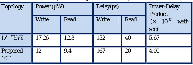
TABLE I: Comparative analysis of 6T and proposed 10T SRAM
Topology Power (µW) Delay(ps) Power-Delay
Product
(× 10-15 watt-sec)
Write Read Write Read
6T (β=2) 17.26 12.3 152 40 5.67
Proposed 10T
12 9.4 167 20 4.00
Here by assuming equal probabilities of write ‘0’ and write ‘1’ operations. During write operation of conventional 6T SRAM cell, BL and BLB are loaded with complementary data and after that charged values are floated. During write operation, it is assumed that the one of the charged value is discharged.. So during a write operation power dissipation happens twice. In case of write operation of proposed 10T SRAM cell, single bit-line is used and it is charged if the data need to be written is ‘1’ and it is not charged to write ‘0’. After the write ‘1’ operation, BL is discharged. So power dissipation is almost half as compared to conventional 6T SRAM Cell. During read operation of 6T SRAM Cell, both the bit-lines are charged to VDD and one of the bit lines will discharge regarding to the value stored in the cell and remaining bit line will be discharged after the operation is completed. So in read operation power dissipation is four times. In proposed 10T SRAM cell seperate 5T is used for read operation. Hence power consumed during read operation is half compared to power consumption in conventional 6T SRAM cell.
B. Static Noise Margin(SNM)
Figure 4.1(a) Butterfly curve to evaluate Figure 4.1 (b) Butterfly curve to evaluate RSNM RSNM for proposed 10T SRAM cell for conventional 6T SRAM cell.
Figure 4.2 (a) Butterfly curve to evaluate HSNM for Figure 4.2 (b) Butterfly curve to evaluate HSNM of proposed 10T SRAM cell 6TSRAM cell
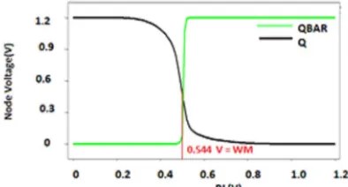
In this work, for WM calculation bit-line voltage sweep method has been chosen. WM is defined as the value of bit-line voltage where Q and QBAR flip. The final WSNM is the minimum value of WM for writing logic“1” and writing logic “0”. If lower is the
[image:5.612.114.502.79.274.2] [image:5.612.87.514.104.510.2] [image:5.612.213.410.602.708.2]TABLE Comparative Analysis of RSNM, WM and HSNM between conventional 6T and proposed 10T SRAM cells architectural designs at 1.2V at 45nm
Topology RSNM
(mV)
WM (mV)
HSNM (mV)
6T (β=2) 170 460 420
Proposed 10T 420 544 430
V. CONCLUSION
With the aim of low power and high SNM, proposed 10T and conventional 6T SRAM cell architectural designs are simulated, analysed and compared. 10T SRAM cell with single bitline consumes 21.4µW power which is 38.1% less than conventional 6T SRAM cell with 29.56µW power. In case of read power consumption, 10TSRAM cell with single bitline consumes 9.4µW which is 23.57% less than conventional 6T SRAM cell with 12.3 µW. 10TSRAM cell with single bitline has quite high RSNM that is 420mV which is 2.47 times more than 6T SRAM cell with 170 mV. The WM of 10T SRAM cell with single bitlineis 544mV
which is 1.14 times more as compared to conventional 6T SRAM cell with 460mV. The HSNM of 10T SRAM cell with single bitline is 430 mV which is 1.05 times more as compared to conventional 6T SRAM cell with 420mV
REFERENCES
[1] M.Moghaddam , M.H. Moaiyeri, M. Eshghi, “Ultra Low Power 7T SRAM Cell Design Based on CMOS”, 23rd Iranian Conference on Electrical Engineering , pp.1357-1361, 2015.
[2] H. Farkhani, A. Peiravi, F. Moradi, “A New Write Assist Technique for SRAM design in 65nm CMOS technology”, Integration, The VLSI Journal, vol. 50, pp.16-27, 2015.
[3] P. Upadhyay, R. Kar, D. Mandal and S.P. Ghoshal, “A Design of Low Swing and Multi Threshold Voltage based Low Power 12T SRAM cells”, Computers & Electrical Engineering, vol. 45, pp. 108-121, 2015.
[4] S.S. Jahromi, R. Bounik,“Power Reduction of 7T Dual –Vt SRAM Cell Using Forward Biasing, Design and Test Symposium, pp.1-4, 2013.
[5] P.Upadhyay, S.K.Chhotray, R.Kar, D.Mandal, S.P.Ghoshal“Write Stability Analysis of 8-T novel SRAM Cell for High Speed Application”,3rd International Conference on Advance Computing , pp.1564-1567, 2013.
[6] S.Jain,K.Santhosh, M.Pattanaik, B.Raj,"A 10T SRAM Cell with inbuilt Charge Sharing for Dynamic Power Reduction”, International Conference on Advances in Technology and Engineering , pp.1-6, 2013.
[7] B. Madiwalar, B.S. Kariyappa, “Single Bit-line 7T SRAM Cell for Low Power and High SNM”, International Multi-Conference on Automation, Computing, Communication, Control and Compressed Sensing ,March 2013, pp.223-228.
[8] K. Sarfraz and V. Kursun “Characterization of a Low Leakage Current and High-Speed 7T SRAM Circuit with Wide Voltage Margins”, IEEE Computer Society Annual Symposium on VLSI, pp.64-69, 2013.
[9] T. Azam, B. Cheng, D. R. S. Cumming, “Variability Resilient Low Power 7T –SRAM Design for Nano-Scaled Technologies”, 11 th International Symposium
on Quality Electronic Design ,pp.9-14, 2010.
[10] Z. Liu and V. Kursun, “Characterization of a Novel Nine-Transistor SRAM Cell”, IEEE Transaction on Very Large Scale Integration Systems, vol. 16, no.4, pp.488-492, 2008.