A NOVEL VLSI BASED CRYPTOCODING TECHNIQUE
USING ERROR CONTROL ALGORITHM
1
B. SENTHILKUMAR, 2V. RAJAMANI
1Research Scholar, Department of Electrical and Electronics Engineering, St. Peter’s University, Avadi,
Chennai, Tamilnadu, INDIA – 600054.
2Principal, Veltech Multitech Dr.Rangarajan Dr.Sakunthala Engineering College, Avadi, Chennai,
Tamilnadu, INDIA – 600062.
E-mail: [email protected] , 2 [email protected]
ABSTRACT
This paper presents a hardware implementation for Encoder and Decoder of the cryptography technique using versatile Error Control Algorithms of Block Codes used in wireless communication networks. This work is focused on the designing of VLSI based hardware implementable and more secured alternative of existing software based symmetric cryptography techniques using DES (Data Encryption Standard) and AES (Advanced Encryption Standard Algorithm). In this design process, traditional methods of sub key generation using bit shifting along with modulo 2 addition, performance of padding and puncturing the bits of words are done so as to maintain the reliability of the design at par with conventional technique. In this design, (7,4) Block code with hamming code algorithm is considered as it has very low probability to retrieve originality without specific syndrome analysis and can be easily penetrated between any number of bits of original message as required by the Cryptography. This design is simulated and the synthesis report is generated using Verilog coding of Xilinx ISE software and the modules and results are illustrated. The report and result reveals that the proposed design will occupy very lesser number of components with reliable performance. This will lead to the small amount of power consumption and compactness in hardware implementation. Also, it is observed that the even though the used key size is small, the complexity for the intruder to retrieve the original message is greatly increased by incorporating the variety of hardware diversifying practice without sacrificing the strength of required cryptography technique. The test result shows the significance of the proposed design as the same set of message never produces the same set of cipher text. So that the computational attacks using software based iteration can not be used to track the plain text.
Keywords: Cryptography, Error Control Algorithm, Block Code, VLSI architecture, Encoder and Decoder
1. INTRODUCTION
Nowadays, without any compromise, the necessity for finding solutions to secure the data storing or transferring the information has become inevitable part of human life. However, always there has been always a threat [1] to the existing cryptography techniques due to the mathematical advancements in computer technologies. At present, the fastest growth of communication systems provide the way to access the enormous amount of information and to provide the variety of means to exchange personal or private data among all kind of the personnel in their working domain. Therefore, every single transmitted bit of information needs to be processed into an unrecognizable form in order
like RSA (Rivest, Shamir and Adleman)
Algorithm[3], the discrete logarithm problem like traditional and elliptic curve Diffie-Hellman are used and their hardware implementation analysis were described.
However, advanced computers, which can process million of key iterations per second, can potentially break most of all conventional cryptosystems [4] actually deployed in practice based on the integer factorization problem (like RSA) or the discrete logarithm problem (like traditional or elliptic curve Diffie-Hellman and DSA, and also all of pairing-based cryptography). But, certain classical cryptosystems [5], whose computational problems are entirely different [6] from the above and potentially much harder to solve, remain largely unaffected by the threat of advanced computing. They are lattice-based cryptosystems and syndrome-based cryptosystems.
In this paper, a novel implementation of syndrome based cryptosystems is discussed. Here, two set of keys are used to prepare the cipher text and its retrieval of original message by code generator and codeword finder respectively. This provides multi-layer security with multiple keys for the proposed cryptosystem. Since, the key size is increased with split key application technique, it shows reliable security strength against known attacks. The proposed design is done by using a high-level hardware description language (Verilog) combined with the usage of FPGA technology.
The complete design is synthesized, using Xilinx ISE 13.1 software simulation tool, for target FPGA device namely XC3S100E -5 vq100 of Spartan3E family. The rest of the paper is organized as follows: Section 2 describes about the existing software based secured data distribution system and proposed hardware based data distribution system. Section 3 will give experimental framework and results. Section 4 will give the conclusions.
2. BACKGROUND AND PRELIMINARIES
2.1. Previous Works on Cryptography
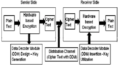
Figure 1 shown below illustrates the existing method of data distribution mechanism. There are two types of techniques adopted in the present software based cryptography namely Private Key Cryptography and Public Key Cryptography. In both methods, original or plain text is converted into cipher text along with generation of alphanumeric key using some standard algorithms like AES and RSA as an encryption process at sender side. These cipher text is converted into
[image:2.595.311.508.168.267.2]plain text by using same key for private key encryption or different key for public key encryption at the receiver side.
Figure 1: Existing Secured Data Distribution System
A lot of research and development works are still going on over DES and Triple DES. Also, DES and Triple-DES [7] are already implemented in Spartan –II devices. It has been found that many attacks are already being enforced to these existing algorithms [8] and some of them have effectively traced the cipher text to retrieve the plain text within the stipulated time bound.
Because of the above constraints, an alternative and efficient encryption and decryption algorithm along with the reliability is always being the thrust for today’s cryptography researchers to enhance the secured data storage and communication domain. In this paper, towards the contribution of finding new reliable cryptography technique, the novel method of hardware implementable cryptography technique based on coding theory algorithm [9] is described for a replacement of existing algorithms like AES and RSA.
Figure 2: Proposed Secured Data Distribution System
[image:2.595.312.511.521.631.2]This encoder converts the original text into
cipher text based on the error control algorithm adopted in the implementation of encoder design. After the completion of successful conversion from plain text to cipher text at sender side, based on the algorithm used, a unique data decoder module (DDM) along with the hardware key will be designed. This module will be the best and reliable
replacement of existing software based
alphanumeric key. Since this hardware based key module is designed by VLSI technology, the distribution of such a unit is easiest one. Also, unlike existing software based alphanumeric key, this hardware based key is untraceable and unreadable by any intruder. This data decoder module will be used at the receiver side to convert the cipher text into plain text.
The followings are main advantages of the above proposed design. Data Decoder Module (DDM) would not be comprehensible to every one as VLSI based hardware has never been easily traceable even for hardware and software professionals. So, reproduction and distribution of hardware based key of DDM by the intruder could be highly impossible. If a dedicated hardware module is used for both encryption and decryption process that would significantly reduce data handling burden of main CPU as well as reduces the required memory size since the software is not used here for cryptography. Such a case, performance of the main processor would be increased while doing decryption. Above all, DDM design is based on modern Error Control Coding Theory which is the entirely new approach for cryptographic technique. So, cipher text framed by proposed system cannot be manipulated easily by an intruder with the help of existing well known attacks.
2.2. Design Methodology for Proposed System
The error control algorithm is mainly used in wireless communication engineering where the original message is transmitted over a channel. This message is checked for any erroneous at the receiver end and if any error happened, it is being identified and corrected by coding theory. This concept is effectively used for the proposed design, as the plain text is purposefully punctured at the encryption process to make cipher text at the encoder side, based on the limitations of chosen block length and the corresponding error control algorithm is used at the decoder side to get back the plain text as the decryption process.
2.2.1. Hardware design for encryption process
Figure 3 shows the hardware design for the encryption process. Even though the proposed system is hardware based one, the traditional methods of software based process such as permutation, substitution, shifting of rows and columns are still incorporated as these steps are used to penetrate bit changing progression throughout the data encryption process.
Initially, the user friendly plain text converted into ASCII equivalent binary values by using C compiler and these ASCII characters are shuffled by the segregating the original equivalent binary bits of original text into several blocks of 2 bit words. For example, an 8 bit binary word can be separated into two 4 bit binary words. These two words further can be separated into four 2 bit binary words. Then, these blocks are rearranged in rows and columns in such a way that it can not be predictable by any intruder. Further, these sets are replaced by different sets of 2 bit binary blocks by means of a predefined look up tables so as to make a distinct from the original text message. After that, extra bits are added to the each block of words according to the type of coding theory based algorithm used. As a next step, bit inversion is made randomly on the block of words but limited to the maximum error correction capability of the algorithm used.
Some more bits are prefix to the each of existing block to identify the type of algorithm used at the decoder stage. This will be more useful when more than one algorithm is used for encoding and decoding process. This technique also increases the confidentiality of the proposed cryptography by hiding the original message further. Finally, shifting of rows and columns of blocks either by left side or right side is done based on the value of key used. So for, there are six steps are used. It is proposed that the initially 24 bit key will be used as each four bit of key representing each one step. This small key size is selected by considering that the design of microchip based on the key size after
successful implementation of proposed
cryptography technique. At the outcome of overall encoder design process, cipher text will be in the binary text format. So, the suitable interfacing software like C compiler can be used to store or write the information into destination storage devices like hard disc and compact disc.
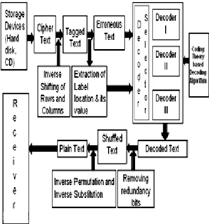
2.2.2. Hardware design for decryption process
the labeling for different block length is made, by [image:4.595.98.286.176.375.2]
appending bits, to identify the block length at the decoder side so as to choose the appropriate decoding algorithm for the same.
Figure.3: Hardware design for Encryption Process
Figure 4: Hardware design for Decryption Process
Design of hardware based Data Decoder Module (DDM) is illustrated in figure 4. This is the hardware key interface module for the proposed system that would replace the existing software based alphanumeric key distribution standard for cryptography technique.
Here, the each and every step is the reverse process of the encoder. The heart of the module is a
set of different decoders along their corresponding decoding algorithms. Based on the key values supplied with microchip, the appropriate decoder would be selected and their corresponding hardware based algorithm will be used to decoding the cipher text and then removing redundancy bit as well as inverse permutation and inverse substitution can be done based on the methods adopted during encryption process. Finally, output of the overall decoder process will have the set of binary values. Suitable software like C compiler can be used to convert the machine language into readable user friendly language to retrieve the original text that is initially fed into the input of proposed encoder module.
3. EXPERIMENTAL FRAME WORK AND
RESULTS
The complete experimental work is carried out in the following manner. In the first phase, proposed design is modeled in Verilog. As the second phase, functional simulation, schematic generation, RTL generation, synthesis for the targeted FPGA device is done using Xilinx ISE Design Suite 13.1i.
The design work is categories into two different phases. First phase is named as Code Generator where the encryption process is carried over to convert original message into cipher text. Second one is named as Codeword Finder where the decryption process is carried over to convert cipher text into original message.
3.1. Design of Code Generator and Codeword Finder
Here the code generator is designed for ASCII characters whose word size is always 8 bits. As the (7,4) block code is used, the 8 bit word is segregated with two 4 bit words so as to penetrate the more puncturing bits with appropriate algorithm. Then three batches of keys, each having 8 bit length, are simultaneously applied to do the necessary work process.
[image:4.595.89.294.405.624.2]Because the algorithm used at the decryption
stage will retrieve the data from the puncturing of word as achieved in the case of coding theory of the wireless communication domain at the receiver side.
Figure 5: RTL Schematic of Code Generator
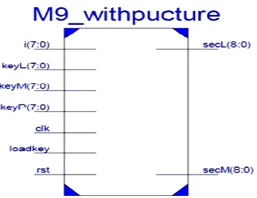
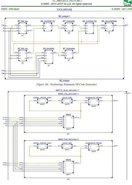
In the figure 6a, each 8 bit word is separated into two 4 bit words and these words are simultaneously treated as per the steps explained in the previous design process. The module M10_parityadder is used to add the parity bit to the set of binary blocks. Modules M11_errormaker and M4_mod2add are used to make the puncturing the binary word by converting binary 1 into binary 0 and vice versa. The two modules M6_codegen is used to produce the two different set of 9 bit values for corresponding one 8 bit original value supplied as input to the module M9_withpucture.
Figure 6b shows the sub modules of the main module of M6_codegen. Here, the two 8 bit modules of M2_8bit_reg are used to store the 8 bit values fed into the input of these modules. The module M3_keyshifter is used to spin the values of from right to left so as to generate the new set of different keys for each stage. This will avoid the generation of same binary value of repeated original text. The other modules M7_keyenabler
and M8_zerocodefinder are simultaneously
employed. That is the module M7_keyenabler supplies the available key values to the input of the module M5_mod2add_3ip only when the output of the module M8_ zerocodefinder is logical 1. The module M8_ zerocodefinder is used to find the end of original text message where the encryption process is to be stopped.
Figure 7 shows the module design for codeword finder. Here, the output of code generator, namely secL and secM, would be given as input to the
module codeword finder namely
MM10_dual_decoder. It should be noted that the
[image:5.595.315.501.163.316.2]same set of keys used for generation of cipher text must be used to get back the original message through codeword finder.
Figure 7: RTL Schematic of Codeword Finder
Also, the same set of cipher texts output of code generator must be fed into the codeword finder as input. Otherwise, there will not be the possibility to have the original message at the output of codeword finder. This complexity in this hardware design upholds the strength of cryptography technique apart from having keys.
In the figure 8a shown above, two identical modules of decoder along with same set of sub
modules namely MM9_full_decoder:1 and
MM9_full_decoder:2 are used. Here the modules parity_check_sum and synd_tab are used to retrieve the original text from the punctured text based on the type of coding theory based algorithm used.
Figure 8b shows the necessary sub modules of MM10_dual_decoder module. The modules MM2 to MM8 are used to do the exactly reverse process of the modules explained in the Figure 6b. If the supplied key to the decoder is same as that of the key used in encoder along with the proper set of 9 bit binary values, the relevant ASCII value of original message will be generated at the output of the decoder module MM10_dual_decoder module. Otherwise, if the supplied keys or set of 9 bit binary files are wrong, the output of the decoder is never able to retrieve the original message.
3.2. Synthesis Report Generated by Xilinx Design Tool
[image:5.595.92.279.185.329.2]utilization summary for existing DES and TDES
algorithms and proposed design using Spartan3 FPGA chip as a target device.
The table1 shows that the proposed system uses minimal number of components to implement the required error control algorithm. This will lead to the low amount of power consumption and heat dissipation at the target device. Because of the usage of less number of components in FPGA implementation, efficient placement and routing can be done using Xilinx synthesis tool. This will further reduce the propagation and line delays so as to improve the overall operational performance of the proposed system.
As shown in the table 1, the proposed system would consume less number of hardware usage for the 128-bit throughput with same type of custom
FPGA chip. So, power consumption and
operational delay of the proposed system is reduced with increased security. However, the choice of code selection is vital to have the trade-off between power consumption of the hardware usage and security of the proposed system. Because, if the length of the codeword of the chosen code is increased, that leads to the increased throughout as well as increased key size. This aspects increase the hardware usage and power consumption in the VLSI implementation.
3.3. Result Generated using Xilinx Simulation Tool
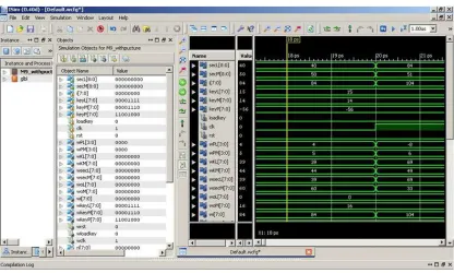
Here the C language program is used to convert the alphanumeric letters into equivalent ASCII binary value and vice versa. The sample word “This is the test of my project.” whose corresponding binary values “84 104 105 115 32 105 115 32 116 104 101 32 116 101 115 116 32 111 102 32 109 121 32 112 114 111 106 101 99 116 46”. It is used to generate the cipher text output of the above work along with key inputs KeyL as 15, KeyM as 14 and KeyP as 200 for the code generator module.
Output generated in the form of binary values is stored in two different file names as secL and secM. The figure 9 shows the simulation output of the code generator module that is used for encryption process of the proposed design.
In the file secL, the binary values “40 84 99 72 0 175 63 0 40 84 1 0 215 61 207 114 0 97 19 0 153 95 0 0 25 110 126 121 184 99 243” are stored. In the file secM, the binary values “50 51 11 112 188 90 210 249 219 204 244 163 111 165 45 42 8 51 11 92 155 81 254 213 219 204 244 132 100 174 1” are stored.
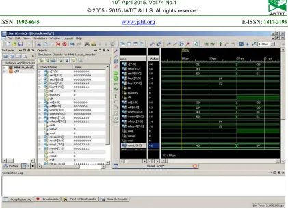
The strength and reliability of above algorithm is tested by changing the input key values such that KeyL as 14 and KeyM as 15 along with same secL and secM data files for codeword finder. The figure 10 shows the simulation output of the codeword finder module that is used for decryption process of the proposed design. Then the output generated is “52 201 77 66 48 41 143 208 228 57 177 224 148 211 125 122 64 207 68 16 125 63 208 128 226 62 190 164 128 203 33”. These values are fed into C compiler to retrieve the original text message.
But, the output word generated is
“4ÉMB0) Ðä9±à”Ó}z@ÏD_}?Ѐâ>¾¤€Ë!”
which is absolutely different from original text message since the value of input keys are different from actually used in code generator module.
4. CONCLUSION
This work was focused on the designing of VLSI based hardware implementable and more secured alternative for existing symmetric key-based cryptosystem. (7,4) Hamming code algorithm was considered in this design process. Sub-key generation by modulo 2 addition, padding and puncturing the bits of words were done so as to maintain the reliability of the design at par with conventional technique. Since two set of keys were used for both code generator and codeword finder, this provides multi-layer security for the proposed cryptosystem. Since, the key size was increased with split key application technique, it would show reliable security strength against brute-force attacks.
In this design, the decoder and encoder modules were successfully designed using verilog hardware descriptive language. Simulation results were generated for the target device 3s100evq100-5 of Spartan3E using Xilinx simulation tool for both code generator and codeword finder. We illustrated an implementation of cryptography using error control algorithm. We presented novel approach of alternative model to implement cryptography technique those are already threatened by many attacks. The proposed chip in the target device
consumed very less amount of hardware
components. Here maximum of 6% of the subcomponents in each section namely slices, flip flops, look up tables and clocks were used to
implement the proposed design. However
maximum of 80% of bonded input and output were used.
However, power consumption and speed of the
module would be taken into consideration. There should be the mild caution while choosing the advanced error control algorithms as it would have
appropriate and less complexity decoding
algorithms that should not be in the case of cryptography technique.
REFRENCES:
[1] Ayoub Otmani, Jean-Pierre Tillich and Leonard Dallot, “Cryptanalysis of Two McEliece Cryptosystems Based on Quasi - Cyclic Codes”, arXiv:0804. 0409v3 [cs.CR], 3 Jan 2010.
[2] Pravin B. Ghewari, Jaymala K. Patil, Amit B. Chougule, “ Efficient Hardware Design and
Implementation of AES Cryptosystem,
International Journal of Engineering Science and Technology”, Vol. 2(3), 2010
[3] Keklik Alptek In Bayam, Berna, “ Differential power analysis resistant hardware implement -tation of the RSA Cryptosystem”, Turk J Elec Eng & Comp Sci, Vol.18, No.1, 2010. [4] Marco Baldi.,” LDPC codes in the McEliece
cryptosystem: attacks and countermeasures”, Polytechnic University of Marche, Ancona, Italy, arXiv:0710.0142v2 [cs.IT], 11 Jan 2009. [5] K.V. Pramod and C. Manju, “A Cryptosystem Using the Concepts of Algebraic Geometric Code”, Journal of Computer Science 6 (3): 244-249, 2010.
[6] P. Kitsos , N. Sklavos and M.D. Galanis, O. Koufopavlou, “64-bit Block ciphers: hardware implementations and comparison analysis”, VLSI Design Lab., Electrical and Computer Engineering Department, University of Patras, Computers and Electrical Engineering , 2004. [7] Prasun Ghosal, Malabika Biswas and Manish
Biswas, “Hardware Implementation of TDES Crypto System with On Chip Verification in FPGA”, Journal Of Telecommunications, February 2010.
[8] Gael Rouvroy, Jean-Jacques Quisquater, and Jean-Didier Legat, “Efficient Implementation of Rijndael Encryption in Reconfigurable Hardware: Improvements and Design
Tradeoffs”, Springer-Verlag Berlin
Heidelberg 2003.
[9] Chetan Nanjunda Mathur, Karthik Narayan, and K.P. Subbalakshmi, “On the Design of
Error-Correcting Ciphers”,Eurasip Journal on Wireless Communications and Networking, Volume, Article ID 42871, 2006
[10] Muzhir Al-Ani and Qeethara Al-Shayea., “Unidirectional Error Correcting Codes for
Memory Systems”, IJCSI International
Journal of Computer Science Issues, Vol. 7, Issue 1, No. 3, January 2010.
[11] Francois -Xavier Standaert, “Secure and
Efficient Implementation of Symmetric
Encryption Schemes using FPGAs”,
Fran¸cois-Xavier Standaert, UCL Crypto Group, 2008.
[12] Pierre-Louis Cayrel and Falko Strenzke,”Side channel attacks in code-based cryptography, First International Workshop on Constructive Side-Channel Analysis and Secure Design , COSADE 2010.
[13] Matthieu Finiasz, “NP - completeness of
Certain Sub-classes of the Syndrome
Decoding Problem”, arXiv : 0912.0453v1, [cs.CR] 2 Dec 2009.
[14] D. Engelbert, R. Overbeck, and A. Schmidt, J. Math, “A Summary of McEliece-Type Cryptosystems and their Security”, 151–199, DOI 10.1515 / JMC.2007.009, 2007.
[15] Paris Kitsos and Odysseas Koufopavlou, “Configurable Hardware Implementations of
Bulk Encryption Units for Wireless
Figure .6b: Technology Schematic Of Code Generator
[image:9.595.86.504.90.361.2]
[image:10.595.90.506.411.661.2]
. Figure 8b: Technology Schematic Of Codeword Finder
Figure 10: Simulation Output Of Codeword Finder
Table 1: Device Utilization Summary Of Existing And Proposed Crypto Systems
Specifications Existing Encoder (Code Generator) Proposed design
Code Generator Codeword Finder
Selected Device Spartan 3 (xc3s400fg320-5)
Spartan 3
(xc3s1000fg67-5)
Spartan3E (3s100evq100-5)
Spartan3E (3s100evq100-5)
Crypto
Algorithm DES[7] TDES[7] Block Code (7,4)
Number of Slices
442 out of 28800
5%
1585 out of 7680 20%
61 out of 960 6%
36 out of 960 3%
Number of Slice Flip Flops
281 out of 28800
1%
1254 out of 15360 8%
46 out of 1920 2%
44 out of 1920 2%
Number of 4 input LUTs
789 out of 15681
5%
2494 out of 15360
16% 98 out of 1920 5% 62 out of 1920 3%
Number of bonded IOBs
190 out of 391
48%
302 out of 391 77%
53 out of 66 80%
45 out of 66 68%
Number of GCLKs
1 out of 8
12%
1 out of 8
12%
1 out of 24 4%
[image:11.595.86.503.449.715.2]