Novel High Speed Low Power Binary Multiplier Designs
using Reversible Logic Gates
Naman Sharma
Bharati Vidyapeeth’s College of Engineering, New Delhi-110063
Upanshu Saraswat
Bharati Vidyapeeth’s College of Engineering, New Delhi-110063
Rajat Sachdeva
Bharati Vidyapeeth’s College of Engineering, New Delhi-110063
ABSTRACT
Reversible logic is highly useful in nanotechnology, low power design and quantum computing. The paper proposes efficient MOS implementation for the basic reversible gates namely, Feynman, Toffoli, and Peres gates and employs the proposed circuits in the reversible binary multiplier design. It also juxtaposes the three proposed architectures to compare their properties and hence propose the most optimized form of the aforementioned multipliers.
General Terms
Reversible logic, Vedic multiplier, Quantum computing.
1.
INTRODUCTION
The tremendous advancements in VLSI technology have led to an increased demand for small sized high performance portable devices. With the size of the chip being reduced, power consumption has become the paramount concern during design considerations. Many techniques such as voltage scaling, to reduce the power consumption of circuits are suggested but their use results in incremental improvements only [17]. It is predicted that the Moore’s law is at an end due to the inability of the designers to keep up with the power requirements of the future chips. [1]
One of the solutions to meet the low-power requirement of the future devices is by adopting an entirely new model known as reversible logic in contrast to the existing irreversible logic. Reversible logic finds its origins in the concepts of Quantum Computing [18]. Researchers like Bennett showed that the devices based on reversible computing consume much less power than the traditional irreversible devices [3][4]. Reversible logic gates use one-to-one mapping between input and output vectors, thereby preventing loss of information, which in turn results prevents dissipation of energy, as shown by Landauer [5][6]. Different arithmetic circuits such as Adders, Subtracters, Multipliers, Carry Adders etc. based on reversible are available in literature. This paper focuses on the implementation of the vedic multiplier in reversible logic.
The essence of Vedic Mathematics lies in the fact that it is one of the most potent tools available to simplify extremely laborious mathematics [7]. Vedic mathematics, is broadly used in reference to a series of 16 mathematical tricks that often make calculations simpler [7][8]. By reducing the number of steps involved, it greatly reduces computational time and at the same time improves accuracy. In this paper, the authors focus on the vedic multipliers. These multipliers in contrast to the traditional multipliers like array multiplier, Booth multiplier, Wallace Tree multiplier etc., are area efficient, low power dissipating and exhibits high speed/low latency [9].
In this paper, the authors propose two new architectures to implement a reversible 2X2 vedic multiplier. The paper first briefly provides an overview of the reversible logic and few reversible gates in section II. Thereafter, the two architectures to implement 2X2 reversible vedic multiplier is proposed in section III. The correctness of the proposed architectures is demonstrated through functional verification in Verilog and the synthesis report on FPGA is also presented in section IV. A performance comparison between the two architectures is also carried out. Finally section VI concludes the paper.
2.
BASIC REVERSIBLE GATES
In 1960, researcher R. Landauer demonstrated that circuits using irreversible hardware results in energy dissipation of kTln2 Joules due to one bit loss of information where k is Boltzmann’s constant and T the absolute temperature [5][6]. Bennett showed that this energy loss can be avoided by constructing circuits using reversible logic gates [3][4] . A reversible logic gate is an n-input, n-output logic function that maintains a one-to-one mapping between the two.
Based on this principle, different basic reversible gates such as Feynman [11], Toffoli [12] and Peres [14] have been proposed. A 2*2 Feynman gate (or a Controlled NOT (CNOT)) with inputs (A,B) produces the output P equal to input A while output Q as the XOR of the inputs as shown in Fig. 1a. A 3*3 Toffoli gate with inputs (A, B, C) and outputs (P, Q, R) is shown in Fig. 1b. It has outputs P and Q equal to A and B respectively while the output R is complement of the input C if both A and B are at logic 1, otherwise it is input C. A Peres gate is a 3*3 reversible gate with inputs (A, B, C) and outputs (P, Q, R). The output P is equal to A; output Q is the XOR of A and B while R is complement of the input C if both A and B are equal to 1, otherwise it is equal to input C. A BVF gate [15] is a 4*4, reversible, double XOR gate and can be used for the duplication of the required inputs to meet the fan-out requirements.
3.
VEDIC MULTIPLIER
Vedic Multiplication greatly simplifies the traditional multiplication process by reducing the number of steps or calculations needed to obtain the products. This vedic multiplication process greatly decreases computation time and hence makes the circuit faster. The technique used to implement the vedic multiplication in the paper is known as Urdhva-Tiryagbyham [7][8].
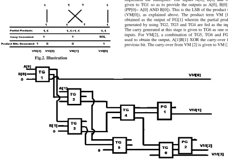
The method to calculate the product of two 2-bit numbers A[1:0] and B[1:0] using Urdhva-Tiryagbhyam approach is illustrated in
Fig. 2. The partial product and the final product are represented as PP [2:0] and VM [3:0] respectively.
Fig.1. Vedic multiplication method for two bit binary numbers
[image:2.595.54.526.409.738.2]The first partial product PP[0] is calculated by the vertical AND of A[0] and B[0] and PP[0] is treated as the LSB of the final product VM[0]. The partial product bit PP[1] and PP[2] is calculated by crosswise AND of the bits. The binary addition of these partial products that is PP[1] and PP[2] generates intermediate carry and sum bits denoted as C1S1. The last partial product term PP[3] is calculated by vertical AND of A[1] and B[1]. The addition of PP[3] and C1 generates next level sum and carry bits as C2S2. The two intermediate sum bits S2, S1 are treated as the VM[2], VM[1] of the final product respectively. The output carry C2 is taken as the MSB of the final product VM[3]. The same has been explained through an example shown in Fig. 6.
Fig.2. Illustration
In this paper, different architectures to implement 2*2 reversible vedic multiplier are proposed. The first architecture (Arch-1) proposes the use of Feynman and Toffoli gates. In the second architecture (Arch-2), Toffoli and BVF Gate are used while in the last architecture (Arch-3), the implementation using Toffoli and Peres Gate is proposed.
3.1
Architecture 1 (Arch-1): 2*2 Vedic
Multiplier using Toffoli and Feynman
Gates
The Arch-1 employs six Toffoli gates, TG(1-6)and two Feynman gates , FG (1,2) in manner shown in Fig. to implement the multiplier. The inputs A[0], B[0] and 0 are given to TG1 so as to provide the outputs as A[0], B[0] and (PP[0]= A[0] AND B[0]). This is the LSB of the product term (VM[0]), as explained above. The product term VM [1] is obtained as the output of FG[1] wherein the partial products generated by using TG2, TG3 and TG4 are fed as the inputs. The carry generated at this stage is given to TG6 as one of the inputs. For VM[2], a combination of TG5, TG6 and FG2 is used to obtain the output, A[1]B[1] XOR the carry-over from previous bit. The carry-over from VM [2] is given to VM [3].
3.2
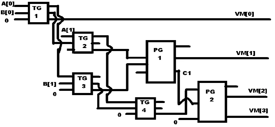
Architecture 2 (Arch-2): 2*2 Vedic
Multiplier using Toffoli and BVF Gate
[image:3.595.53.531.69.331.2]The BVF gate is a Reversible Double XOR gate. This property of the BVF gate is used in the implementation of the multiplier.
Fig. 4. Implementation using Toffoli and BVF gate
The Arch-2 employing six Toffoli gates, TG (1-6)and one BVF, (1) is shown in Fig. . A closer examination of the circuit reveals that the method to generate the partial products is similar as discussed in Arch-1. The difference being, that instead of using two Feynman gates to perform the required XOR operation, the double XOR-ing BVF gate is employed. The BVF gate (BVF1) is given four inputs, namely A[1]B[0], A[0]B[1], carry from previous stage (C1) and A[1]B[1], two of the outputs provide VM[1] and VM[2] of the multiplication process. The bit VM[0] is obtained by TG1 as shown. The bit VM [3] is obtained as the output of the TG6.
3.3
Architecture 3 (Arch-3): 2*2 Vedic
Multiplier using Toffoli and Peres Gate
In this architecture (Arch-3), the use of Peres gate is proposed. A Peres Gate gives outputs in the form, A XOR B and AB XOR C, for three inputs A, B and C. If C is taken as low, then the outputs can be reduced as sum and carry of a two bit number. This property is used in the realization of the multiplier.
Fig. 5. Implementation using Peres gate and Toffoli gate
In the proposed architecture (Arch-3) shown in Fig. 9, only four Toffoli gates (TG1-4) are used in contrast to the six used in Arch-1 and Arch-2. The four Toffoli gates are responsible for producing the partial products bits. These partial products are then given as inputs to the two Peres gates, (PG1,2).
[image:3.595.71.525.480.689.2]4.
SIMULATION SECTION
This section first verifies the functionality of the three proposed architectures (Arch-1, Arch-2 and Arch-3) to implement a reversible 2X2 vedic multiplier. The functionality has been verified through Verilog Simulation. Thereafter, the effectiveness of the proposed architecture is demonstrated through their synthesis on FPGA using Xilinx. In the last, a comparative analysis for the proposed three architectures is performed.
4.1
Functional Verification
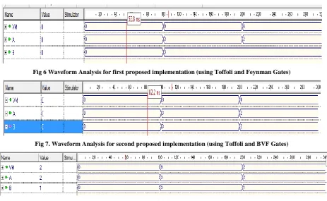
[image:4.595.68.532.170.455.2]The proposed architectures are implemented with Verilog and are simulated for functional verification. The output waveforms for the three architectures of 2X2 vedic multiplier is shown in Fig. 10, Fig. 11, Fig. 12. It can be observed that all of them adhere to the functionality of the multiplier.
Fig 6 Waveform Analysis for first proposed implementation (using Toffoli and Feynman Gates)
Fig 7. Waveform Analysis for second proposed implementation (using Toffoli and BVF Gates)
Fig 8. Waveform Analysis for second proposed implementation (using Toffoli and Peres Gate
5.
PERFORMANCE COMPARISON
[image:4.595.73.526.178.257.2]In this sub-section, the proposed architectures are compared in terms of garbage outputs, constant inputs, gate count and quantum cost. A Gate Count is defined as the number reversible gates required to implement any function. A garbage output is the one which is not connected to any input of the subsequent reversible gates. A constant input is the one which is kept constant throughout the implementation. The comparative analysis is listed Table I. From the comparative analysis, it can be concluded that the Arch-3 is efficient in terms of gate count and the quantum cost than the other two.
Table I. Comparative Analysis
6.
CONCLUSION
Hence, the authors were able to implement a 2*2 Binary Multiplier using Reversible Logic Gates. Upon implementation, it was found that the architectures that we have proposed here have different values of quantum cost, which is an effective measure to check for the amount of power consumed by the circuit.
It was found out that Architecture 3 had the least value for quantum cost, which is 28. And hence this architecture is the most power efficient out of the three.
The uses of Reversible logic gates are especially important because of its application to the field of quantum computers. With Quantum Computing, providing a viable alternative to the classical Digital Computers, several questions come to mind about the implementation of this technology in the near future. First, we need to ask whether a quantum model for computers will be an all-pervasive one, providing applications to the whole gamut of technological requirements of the modern age. Second, whether or not these modern systems will be able to control or remove the problem of Quantum Decoherence, to the extent that such systems can be effectively used in the future. The authors believe that the future of modern computers depends on the answers to these questions.
7.
REFERENCES
[1] Laszlo B. Kish, Texas A&M University, Department of Electrical Engineering, College Station, TX 77843-3128, USA Received 16 July 2002; received in revised form 19 September 2002; accepted 19 September 2002, Communicated by C.R. Doering, “End of Moore’s law: thermal (noise) death of integration in micro and nano electronics.”
[image:4.595.55.263.614.703.2]Laboratory, “Dynamic Voltage Scaling and the: Design of a Low-Power Microprocessor System”
[3] C. H. Bennett, "Notes on the history of reversible computation," IBM J. Research and Development, vol. 32, pp. 16-23, January 1988.
[4] C. H. Bennett, "Logical reversibility of computation," IBM J. Research and Development, pp. 525-532, November 1973.
[5] R. W. Keyes and R. Landauer, "Minimal energy dissipation in logic," IBM J. Research and Development, pp. 152-157, March 1970.
[6] R. Landauer, "Irreversibility and heat generation in the computing process," IBM J. Research and Development, vol. 3, pp. 183-191, July 1961.’
[7] Jagadguru Swami, Sri Bharati Krisna, Tirthaji Maharaja, “Vedic Mathematics or Sixteen Simple Mathematical Formulae from the Veda, Delhi (1965)”, Motilal Banarsidas, Varanasi, India, 1986.
[8] Ramalatha, M.Dayalan, K D Dharani, P Priya, and S Deoborah, “High Speed Energy Efficient ALU Design using Vedic Multiplication Techniques”, International Conference on Advances in Computational Tools for Engineering Applications (ACTEA) IEEE, pp. 600-603, July 15-17, 2009.
[9] Pushpalata Verma, K. K. Mehta, “Implementation of an Efficient Multiplier based on Vedic Mathematics Using EDA Tool”, International Journal of Engineering and Advanced Technology (IJEAT), ISSN: 2249 – 8958, Volume-1, Issue-5, June-2012.
[10] H. D. Tiwari, G. Gankhuyag, C. M. Kim, and Y. b. Cho, ”Multiplier design based in ancient Indian Vedic Mathematics,” in Proceeding IEEE International SoC Design Conference, Bussan, Nov. 24-25,2008,pp.65-68.
[11] R. Feynman,” Quantum Mechanical Computers”, Optic News, Vol 11, pp 11-20 1985.
[12] T.Toffoli, “Reversible Computing”, Tech memoMIT/LCS/TM-151, MIT Lab for Computer Science 1980.
[13] Fredkin E. Fredkin and T. Toffoli,, “Conservative Logic”, Int’l J. Theoretical Physics Vol 21, pp.219-253, 1982
[14] Peres, “Reversible Logic and Quantum Computers”, Physical review A, 32:3266- 3276, 1985.
[15] X. Susan Christina, M.Sangeetha Justine, K.Rekha, U.Subha and R.Sumathi, ―Realization of BCD adder using Reversible Logic‖, International Journal of Computer Theory and Engineering, Vol. 2, No. 3, June, 2010 1793-8201.
[16] N. Rajput, M.Sethi, P.Dobriyal, K.Sharma, G. Sharma, “A Novel, High Performance and Power Efficient Implementation of 8x8 Multiplier Unit using MT-CMOS Technique”, IEEE Explore, 2013.
[17] Padmanabhan Pillai and Kang G. Shin, “Real-Time Dynamic Voltage Scaling for Low-Power Embedded Operating Systems”, Real-Time Computing Laboratory Department of Electrical Engineering and Computer Science The University of Michigan Ann Arbor, MI 48109-2122, U.S.A.