http://dx.doi.org/10.4236/cs.2016.72007
How to cite this paper:Sabaghi, M., Marjani, S. and Majdabadi, A. (2016) The Design of Ultra-Low Power Adder Cell in 90 and 180 nm CMOS Technology. Circuits and Systems, 7, 58-67. http://dx.doi.org/10.4236/cs.2016.72007
The Design of Ultra-Low Power Adder Cell
in 90 and 180 nm CMOS Technology
Masoud Sabaghi1*, Saeid Marjani1,2, Abbas Majdabadi1
1Laser and Optics Research School, Nuclear Science and Technology Research School,
Atomic Energy Organization of Iran, Tehran, Iran
2Department of Electrical Engineering, Ferdowsi University of Mashhad, Mashhad, Iran
Received 12 January 2016; accepted 20 February 2016; published 23 February 2016
Copyright © 2016 by authors and Scientific Research Publishing Inc.
This work is licensed under the Creative Commons Attribution International License (CC BY). http://creativecommons.org/licenses/by/4.0/
Abstract
In this paper, an ultra-low power adder cell is proposed. With cascading two XNOR cells, the sum of two inputs is achieved. Regarding to advantages of m-GDI XNOR cell, we constructed the adder cell based on this architecture. The simulation results show that the power consumption of the adder cell designed with GDI technology is 12.993 µw, whereas for this cell designed with m-GDI technology is 4.1628 µw, which both are designed at 0.18 um technology. Moreover, simulation results in 90 nm CMOS technology for m-GDI adder cell show average power consumption of 0.90262 µw and 6.3222 µw in 200 MHz and 2GHz, respectively.
Keywords
Adder Cell, Gate-Diffusion-Input (GDI), Bit-Serial Adder
1. Introduction
The adders are the most common arithmetic circuits in digital systems as key components of multipliers and di-viders that are used to do subtraction. There are several types of adders with different configurations, speeds and areas that we can select an appropriate one which satisfies our requirements. When information transferring is serial to reduce wiring, the serial adders are generally used [1]-[3]. The adder is one section of comparator (dig-ital-comparator) [4]-[6] and successive approximation ADC control system [7] [8]. Also, the adder implements the delta-sigma analog to digital converter (decimation filter) [9]-[12]. Analog adder circuit is one of important sections in phase locked loop that is used in the cavity to maintain the mode locking conditions for lasers [13]-[22] and VCSELs [23]-[35].
*
converted into heat. In this way, the heat dissipation system and cooling mechanisms become indispensable for the correct, reliable and safe operation of the device. An increase of 10˚C in the working temperature of an elec-tronic device causes a 100% increase in its failure rate. Therefore, it is possible to reduce the associated costs for expensive cooling and complex packaging needs if it is possible to decrease the heat dissipation.
The registers are other undividable parts of serial adders that consist of the latches. The cascading D Flip- flops is the simplest way to build the registers. We can achieve this register by cascading 4 D Flip-Flops since our design goal is a 4-bit adder. Choosing of proper D Flip-Flops is of our interests that beside high reliability, meet our requirements of lower power consumption and high speed. Finally, post-layout simulation will be ac-complished to bring parasitic capacitances existing in the die to account. The paper is organized as follows: Sec-tion 2 briefly describes the serial adder, SecSec-tion 3 provides the details of the proposed ultra-low power full ad-ders, and Section 4 presents the results and discussions. Finally, in Section 5, we conclude.
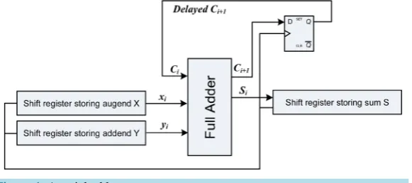
2. Serial Adder
A serial adder operates similarly to manual addition. The serial adder, at each step, calculates the sum and car-ries at one bit position. It starts at the least significant bit position and each successive next step it sequentially moves to the next more significant bit position where it calculates the sum and carry. At the n-th step, it calcu-lates the sum and carries at the most significant bit position. In other words, the serial adder serially adds augend X and addend Y by adding xi, yi, and ci at the i-th bit position from i = 0 to n − 1. We have sum bit
i i i i
s = ⊕ ⊕x y c and carry to the next higher bit position
(
)
1 · ·
i i i i i i
c+ =x y ⊕c x ⊕y
where “·” is AND, “˅” is OR, and “⊕” is XOR, and henceforth, “·” will be omitted. This serial addition can be realized by the logic network, called a serial adder, or bit-serial adder. The addition of each i-th bit is done at a rate of one bit per cycle of clock, producing sum bits, si’s, at the same rate, from the least significant bit to the most significant one. In each cycle, si and ci+1, are calculated from xi, yi, and the carry from the previous cycle, ci.
The core logic network, shown in the rectangle in Figure 1, for this one-bit addition for the i-th bit position is called a full adder (FA).
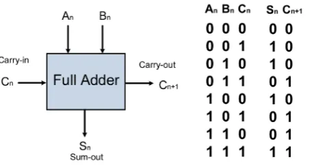
[image:2.595.170.461.583.712.2]The 1-Bit full adder design is one of the most critical components of a processor that determines its through-put, as it is used in ALU, the floating point unit, and address generation in case of cache or memory accesses. The logic symbol and truth table for a full adder circuit are shown inFigure 2. The logic functions for the sum and carry outputs can be written as:
Figure 2.The logic symbol and truth table for a full adder.
i i i i
s = ⊕ ⊕x y c (1)
(
)
(
(
)
)
1 also 1
i i i i i i i i i i i i
c+ = ⋅ ⊕ ⋅x y c x ⊕y c+ = ⋅ ⊕ ⋅x y c x ⊕y . (2)
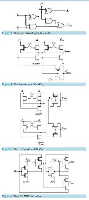
We obtain the logic network for a FA shown in Figure 3using AND, OR, and XOR gates. A D-type flip-flop may be used as a delay element which stores the carry for a cycle [3]. We can obtain this cell using conventional CMOS logics, but it highly suffers from large number of transistors and therefore high power consumption, large occupied are. As a results other structures, with less transistors are proposed.
3. The Proposed Ultra-Low Power Full Adders
3.1. 8 Transistors (8-T) Full Adder
As shown in Figure 4, the 8-T full adder contains three modules-two 3-T XOR gates and a 2-transistor multip-lexer (2-T MUX). Owing to the appealing traits of a small number of transistors and a mere 2-transistor (2-T) delay, it can work at high speed with low power dissipation.
3.2. 10 Transistors (10-T) Full Adder
The 10-T full adder consists of four modules, including one 3-T XOR gate, one 3-T XNOR gate, and two 2-T multiplexers (2-T MUX) as shown inFigure 5. According to the logic equations and the GDI XOR and XNOR gates, full adders can be redesigned in two patterns including GDI XOR full adder and GDI XNOR full adder. Compared to the 8-T full adder, the GDI adders may be slightly slower, since more transistors are used in GDI circuits. As is well known, the number of transistors in circuits can influence performance in many aspects, es-pecially speed.
3.3. GDI (Gate-Diffusion-Input) XOR Full Adder
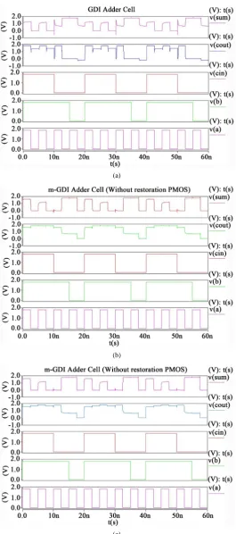
The transistor level implementation of GDI XOR full adder is shown in Figure 6. This full adder consists of three modules-two GDI XOR gates and a multiplexer. In the worst case, Sum has 4-T delay while Cout has 3-T delay. However, due to the advantages of GDI cell, this circuit still can achieve its benefit of low power con-sumption [36]-[38].
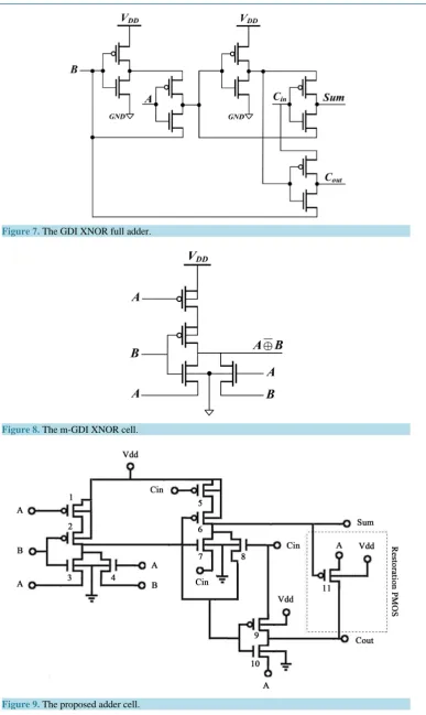
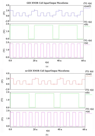
Figure 7 shows the GDI XNOR full adder which is another basic architecture of the application of GDI cells. This scheme also includes three modules. It contains two GDI XNOR gates and a multiplexer. In the worst route, Sum has 4-T delay and Cout has 3-T delay [39]. The other new leaf cells and the circuits built on the basis of GDI technique is presented by P. Balasubramanian et al. and is called m-GDI technique [36]. The structure of a XNOR m-GDI cell is shown inFigure 8.
3.4. The Proposed Adder Cell
Figure 4.The 8 transistors full adder.
[image:4.595.170.459.77.726.2]Figure 5.The 10 transistors full adder.
Figure 7. The GDI XNOR full adder.
[image:5.595.133.494.480.709.2]Figure 8. The m-GDI XNOR cell.
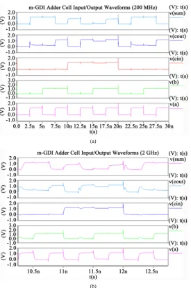
Figure 12. Table 2indicates average power consumption and rise/fall time of m-GDI adder cell in 90 nm tech-nology.
(a)
[image:6.595.149.480.230.704.2](b)
(a)
(b)
[image:7.595.181.447.79.679.2](c)
(a)
[image:8.595.178.454.80.496.2](b)
Figure 12.The m-GDI adder cell input/output waveforms in 90 nm technology (a) 200 MHz; (b) 2 GHz.
Table 1.Comparison of GDI and m-GDI power consumption and delay.
XNOR cell Average power (µw) Rise time (ps) Fall time (ps)
m-GDI 1.2796 50 148
GDI 3.9206 74 213
Table 2. Average power consumption and rise/fall time of m-GDI adder cell in 90 nm technology.
Frequency Average vdd power consumption (µw)
Average inputa power consumption (µw)
Average inputb power consumption (µw)
Average cin power consumption (µw)
Rise time (ps)
Fall time (ps)
200 MHz 0.90262 0.30007 0.17399 0.11401 57 75
2 GHz 6.3222 0.31976 0.19282 0.13620 94 123
5. Conclusion
[image:8.595.85.542.623.678.2]of two inputs, regarding to advantages of m-GDI XNOR cell. The simulation results show that the power con-sumption of the adder cell designed with GDI technology is 12.993 µw, whereas for this cell designed with m-GDI technology is 4.1628 µw at 0.18 µm technology. Also, simulation results show average power consump-tion of 0.90262 µw and 6.3222 µw in 200 MHz and 2 GHz, respectively for m-GDI adder cell in 90 nm CMOS technology.
Acknowledgements
This work was supported by the Laser and Optics Research School, Nuclear Science and Technology Research School, Atomic Energy Organization of Iran, Tehran, Iran.
References
[1] Chen, W. (2007) The VLSI Handbook. CRC Press, FL, USA.
[2] Wang, D., Yang, D., Cheng, W., Guan, X., Shu, X. and Yang, Y. (2009) Novel Low Power Full Adder Cells in 180 nm CMOS Technology. The IEEE Conference on Industrial Electronics and Applications (ICIEA), Xi’an, China, 25-27 May 2009, 25-27.
[3] Gao, H., Qiao, F., Wei, D. and Yang, H. (2006) A Novel Low-Power and High-Speed Master-Slave D Flip-Flop. The IEEE Region 10 Conference (TENCON), Hong Kong, China, 14-17 November 2006, 1-4.
[4] Dashtbayazi, M., Sabaghi, M. and Marjani, S. (2015) Dynamic Comparator with Using Negative Resistance and CMOS Input Pair Strategies in FS = 4 MHz - 10 GHz. Journal of Electrical and Electronic Engineering, 3, 93-96.
http://dx.doi.org/10.11648/j.jeee.20150304.15
[5] Dashtbayazi, M., Marjani, M. and Sabaghi, M. (2015) A 4 MHz - 10 GHz, 10-ps/dec Dynamic Comparator Using Negative Resistance Combined with CMOS Input Pair. The Progress in Electromagnetics Research Symposium (PIERS), Prague, Czech Republic, 6-9 July 2015, 831-834.
[6] Sabaghi, M., Majdabadi, A., Dashtbayazi, M. and Marjani, S. (2015) A 4 MHz - 10 GHz, Dynamic Comparator Using Negative Resistance Combined with CMOS Input Pair Strategy in Dynamic Pre-Amplifier. The Iranian Conference on Optics and Laser Engineering (ICOLE), Isfahan, Iran, 2-3 September 2015, 136-139.
[7] Dashtbayazi, M., Sabaghi, M. and Marjani, S. (2015) An Optimized DAC Timing Strategy in SAR ADC with Consi-dering the Overshoot Effect. Journal of Electrical and Electronic Engineering, 3, 19-24.
http://dx.doi.org/10.11648/j.jeee.20150302.12
[8] Sabaghi, M., Dashtbayazi, M. and Marjani, S. (2016) Dynamic Hysteresis Band Fixed Frequency Current Control.
World Applied Programming, 6, 1-4.
[9] Dashtbayazi, M., Sabaghi, M., Rezaei, M. and Marjani, S. (2014) New Delta Sigma Modulator Structure Using Second Order Filter in One Stage Technique. Journal of Electrical and Electronic Engineering, 2, 82-88.
http://dx.doi.org/10.11648/j.jeee.20140206.11
[10] Sabaghi, M., Dashtbayazi, M. and Marjani, S. (2015) An Optimized Opamp-Sharing in 2nd Order ΔΣ Modulator Based on Changing the Stages Output Capacitance Timing Strategy. The Progress in Electromagnetics Research Symposium (PIERS), Prague, Czech Republic, 6-9 July 2015, 827-830.
[11] Dashtbayazi, M., Majdabadi, A., Sabaghi, M. and Marjani, S. (2015) An Optimized Opamp-Sharing Technique in 2nd Order Delta-Sigma Modulator Based on Changing the Stages Output Capacitance Timing Strategy. The Iranian Con-ference on Optics and Laser Engineering (ICOLE), Isfahan, 2-3 September 2015, 129-131.
[12] Dashtbayazi, M., Marjani, S., Sabaghi, M. and Majdabadi, A. (2016) Changing the Clock Pulse-Width Dedicated to Stages Strategy for Opamp-Sharing Technique in 2nd Order High-Pass Delta-Sigma Modulators. The International Conference on Electrical, Computer, Mechanical and Mechatronics Engineering (ICE), Dubai, United Arab Emirates, to Be Published.
[13] Marjani, A., Marjani, S. and Shirazian, S. (2011) Numerical Simulation of Silicon Carbide Polymers (6H-SiC & 3C- SiC) as the Active Area for 0.83 μm Wavelength Semiconductor Laser. The 14th Iranian Physical Chemistry Confe-rence, University of Tehran, Kish, 25-28 February 2011, 876-878.
[14] Marjani, S., Faez, R. and Marjani, H. (2011) Analysis and Design of Semiconductor Laser with Silicon Carbide Poly-mers (6H-SiC and 3C-SiC). Australian Journal of Basic and Applied Sciences, 5, 1060-1063.
[15] Marjani, S. and Marjani, H. (2012) Self-Heating Effects in a Silicon Carbide Polymers (6H-SiC and 3C-SiC) Semi-conductor Laser. Asian Journal of Chemistry, 24, 3145-3147.
and Experimentation of Copper Vapor Laser. Circuits and Systems, 7, 23-28. http://dx.doi.org/10.4236/cs.2016.71003
[22] Behrouzinia, S., Khorasani, K., Marjani, S., Sabaghi, M., Aeinehvand, M.E. and Mohammadpour Lima, S. (2016) Ex-perimental Study of Buffer Gas Flow Rate Effect on Output Power of a Copper Vapor Laser. Optics and Photonics Journal. (In Press)
[23] Faez, R., Marjani, A. and Marjani, S. (2011) Design and Simulation of a High Power Single Mode 1550nm InGaAsP VCSELs. IEICE Electronics Express, 8, 1096-1101. http://dx.doi.org/10.1587/elex.8.1096
[24] Marjani, S., Faez, R. and Marjani, H. (2011) An Impact of the Hole Etching Depth within a Photonic Crystal VCSEL on Its Heat Sources. Australian Journal of Basic and Applied Sciences, 5, 766-770.
[25] Marjani, S., Faez, R. and Marjan, A. (2011) Design and Modeling of a High Single Mode Power Long Wavelength InGaAsP Photonic Crystal VCSEL. Australian Journal of Basic and Applied Sciences, 5, 1064-1069.
[26] Marjani, S., Rahnama, M. and Marjani, H. (2011) Numerical Optimization of Single-Mode InGaAsP Vertical-Cavity Surface-Emitting Lasers. Australian Journal of Basic and Applied Sciences, 5, 1207-1211.
[27] Marjani, S. and Marjani, H. (2011) Effects of Lattice Temperature on the Various Elements of Heat Sources in a Long Wavelength InGaAsP Photonic Crystal VCSEL. Australian Journal of Basic and Applied Sciences, 5, 1257-1261. [28] Marjani, S. and Marjani, H. (2011) Analysis of Lattice Temperature Effects on a Long Wavelength InGaAsP Photonic
Crystal VCSEL. Australian Journal of Basic and Applied Sciences, 5, 1374-1378.
[29] Marjani, S. and Marjani, H. (2012) Optimization of a Long Wavelength Vertical-Cavity Surface-Emitting Lasers by Employing Photonic Crystal. Asian Journal of Chemistry, 24, 3174-3176.
[30] Marjani, S. and Marjani, H. (2012) Effects of Hole Etching Depth in a Long Wavelength InGaAsP Photonic Crystal Vertical Cavity Surface Emitting Laser. Asian Journal of Chemistry, 24, 3194-3196.
[31] Marjani, S. (2013) Various Elements of Heat Sources within an Optimized Photonic Crystal Vertical Cavity Surface Emitting Laser: Influence of Hole Etching Depth. Asian Journal of Chemistry, 25, 4153-4156.
[32] Marjani, S. (2013) Optimization of an InGaAsP Vertical-Cavity Surface-Emitting Diode Lasers for High-Power Sin-gle-Mode Operation in 1550 nm Optical-Fibre Communication Systems. Asian Journal of Chemistry, 25, 4150-4152. [33] Marjani, S., Faez, R. and Hosseini, S.E. (2013) Threshold Characteristics Analysis of InP-Based PhC VCSEL with Bu-ried Tunnel Junction. The 21st Iranian Conference on Electrical Engineering (ICEE), Ferdowsi University of Mashhad, Mashhad, 14-16 May 2013, 1-4. http://dx.doi.org/10.1109/iraniancee.2013.6599783
[34] Majdabadi, A., Marjani, S. and Sabaghi, M. (2014) Threshold Characteristics Enhancement of a Single Mode 1.55 μm InGaAsP Photonic Crystal VCSEL for Optical Communication Systems. Optics and Photonics Journal, 4, 296-303.
http://dx.doi.org/10.4236/opj.2014.410029
[35] Naeemi, M.A., Marjani, S. and Peiravi, A. (2014) Time to Failure Analysis of Single Mode Long-Wavelength In-GaAsP Vertical-Cavity Surface-Emitting Lasers. The 22nd Iranian Conference on Electrical Engineering (ICEE), Shahid Beheshti University, Tehran, 20-22 May 2014, 43-47. http://dx.doi.org/10.1109/iraniancee.2014.6999500
[36] Balasubramanian, P. and John, J. (2006) Low Power Digital Design Using Modified GDI Method. The IEEE Interna-tional Conference on Design and Test of Integrated Systems in Nanoscale Technology (DTIS), Tunis, 5-7 September 2006, 190-193. http://dx.doi.org/10.1109/dtis.2006.1708713
[37] Morgenshtein, A., Fish, A. and Wagner, I.A. (2002) Gate-Diffusion Input (GDI): A Power-Efficient Method for Digital Combinational Circuits. IEEE Transactions on Very Large Scale Integration (VLSI) Systems, 10, 566-581.
http://dx.doi.org/10.1109/TVLSI.2002.801578
[38] Morgenshtein, A., Shwartz, I. and Fish, A. (2010) Gate Diffusion Input (GDI) Logic in Standard CMOS Na-Noscale Process. The IEEE Convention of Electrical and Electronics Engineers in Israel (IEEEI), Eilat, 17-20 November 2010, 000776-000780.
[39] Mukherjee, B. and Ghosal, A. (2015) Design & Study of a Low Power High Speed Full Adder Using GDI Multi-Plexer. IEEE International Conference on Recent Trends in Information Systems (ReTIS), Kolkata, 9-11 July 2015, 465-470.