Enhanced Buffer Router Design in NOC
Bhavana Prakash Shrivastava
Assistant Professor Electronics Department
Maulana Azad Institute of Technology Bhopal India
ABSTRACT
This paper presents an advance router design using enhanced buffer. The design provides advantages of both buffer and bufferless network for that two cross bar switches are used. The concept of virtual channel (VC) is eliminated from the previous design by using an efficient flow-control scheme that uses the storage already present in pipelined channels in place of explicit input virtual channel buffers (VCBs).This can be addressed by providing enhanced buffers on the bufferless link and creating two virtual networks. With this approach, VCBs act as distributed FIFO buffers. Without VCBs or VCs, deadlock prevention is achieved by duplicating physical channels. An enhanced buffer provides a function of hand shaking by providing a ready valid handshake signal and two bit storage. Through this design the power is saving to 18.98% and delay is reduced by 99.13% as compared with the generic router and the power is saving to 15.65% and delay is reduced to 97.88% as compared to virtual channel router.
General Terms
Router design, Virtual channel, Buffer architecture, Virtual Channel Allocation.
Keywords
NOC, Gate delay, VCs, enhanced buffer, VCB.
1. INTRODUCTION
With the advancement in IC technology the gate delay decreases which leads to relatively increase the wire delay. The wire delay decides the overall performance of the system. Many VLSI designers are trying to solve this long global wire delay problem through buffer insertion. Many current System-on-Chips (SoCs) use a system bus to connect several functional units. These SoC system buses can support only limited number of functional units, and thus will face scaling problems in heterogeneous Multiprocessor System-on-Chips (MPSoCs) or large scale Chip-Multiprocessors (CMPs). In order to solve these long global wire delay and scalability issues, many studies suggested the use of a packet based communication network which is known asNetwork-on-Chip (NoC). This NoC is used to connect many functional units with a universal communication network [1, 2, 3]. In today’s NoCs researchers are continuously confronted by several major challenges: reducing power dissipation in the network, improving performance etc.The power consumed by modern NoCs consists of a large portion of total chip power. For example, 28% of the total chip power of Intel Teraflops processors is spent for communication, while the expectation was only 10 % [12]. Moreover, the interconnection network of MIT’s RAW processor consumes 36% of the total chip power [13, 14]. Power dissipation in modern NoC architectures is
Kavita Khare
Associate Professor Electronics Department
Maulana Azad Institute of Technology Bhopal India
mainly characterized by the power consumed in the links, crossbars, and input buffers. Input buffers alone could consume up to 30-35% percent of the total power of the whole interconnection network [11]. As a result, reducing the size of input buffers or completely eliminating input buffers is a natural approach to design low-power NoCs. Simply reducing the size of input buffers in each router may result in a degraded performance such as reduced throughput etc. Different types of techniques have been proposed to reduce the size of input buffers or to eliminate them.
1.1
Related Work
1.1.1
Generic NOC Router
The router implemented using wormhole is Generic NoC router shown in Figure 1.It has five inputs and output ports, each of which is for local processing element (PE) and four directions: North, South, West, and East. Each router also has five components: Routing Computation (RC) Unit, Virtual Channel Allocator (VA), Switch Allocator (SA), flit Buffers (BUF), and Crossbar Switch.
When the header flit arrives at the buffer, the RC unit sends incoming flits to one of physical channels. The Virtual Channel Allocation(VA) unit receives the credit information from the neighboring routers, arbitrates all the header flits which access the same VCs, and then one of them was selected. Therefore, this header flit can set up the path and then send data. The transmitting router sends the control information to the receiving router, and receiving router may update VC information at the internal buffer with this control information. SA unit arbitrates the waiting flit in all VCs accessing the crossbar and allow only one flit to access crossbar .The SA operation is based on the VA stage since the flit data in the buffer comes from the previous router in the route. The flit data pass over the crossbar and thus can arrive at the destination node.
1.1.2
Virtual Channel Regulator (ViChaR)
The router implemented using virtual channel is ViChaR [7].This can efficiently allocating buffers to all virtual channels, instead of using separated buffers, a unified buffer structure (UBS) is used to share the internal flit buffers and Unified Control Logic (UCL,) to control UBS and assign buffers into VCs dynamically according to the network traffic [11]. Figures 2 (a, b) show the comparison between the ViChaR router buffer architecture with generic router buffer architecture. It is shown in the Figures 2(a, b) that UBS is similar to generic buffer structure in which the v independently k- flit are logically grouped in a single vk-flit and with UCL as logically unified structure. To avoid large components UBS has the same number of MUX/DEMUX i.e. one MUX/DEMUX per k flits. In the shown Figure 3(a) the first stage reduces the number of requests from each input VC to one and the winning request from each input VC proceeds to the second arbitration stage.
Input port 1
Input port P
Routing Computation (RC)
VC Allocator (VA)
VC Identifier
VC 1
VC v
Crossbar (P×P) Input
Channel 1
Input Channel
P
Output Channel
1
Output Channel
P Credit In
Credit Out
Switch Allocator (SA) Credit
Out
BUF
Figure 1: Generic NOC Router
Figure 2 (a): Buffer architecture and allocation of generic router
Flit 1 Flit 2 Flit 3
Flit k
Control logic VC1
VC identifier SA Control
Flit 1 Flit 2 Flit 3
Flit k
Control logic VC v
VC identifier SA Control VC
Identifier
SA Control I
n p u t
D E M
U X
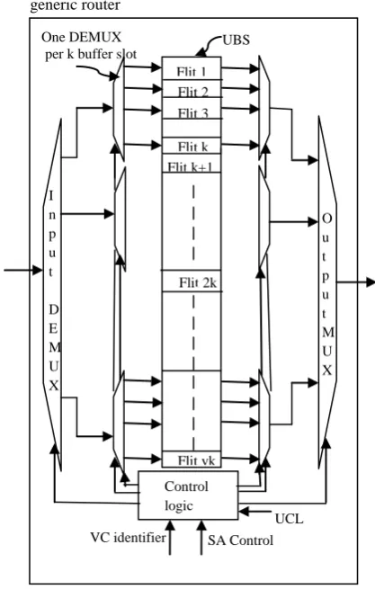
Figure: 2 (b)-Buffer architecture and allocation of ViChaR router
O u t p u t M U X
Input port p Generic Buffer
Figure2 (b): Buffer architecture and allocation of ViChaR router
Flit vk
Control logic
VC identifier SA Control I
n p u t
D E M U X
O u t p u t M U X Flit 1
Flit 2 Flit 3
Flit k Flit k+1
Flit 2k One DEMUX
per k buffer slot
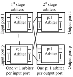
[image:2.595.326.531.75.396.2] [image:2.595.63.288.180.357.2] [image:2.595.322.531.406.734.2]While in Figure 3(b) the first arbitration stage reduces the number of requests for a particular output port to one request per input port.In generic router implementation of VA first stage needs v: 1 arbiter as the number of VCs supported is fixed to v while in case of ViChaR the VA first stage needs vk:1 arbiter but in second stage a winner for each output port among all the competing input ports. So it just allocates the VCs instead of accepting requests for specific VCs.
Similarly the SA in Figure 4(a, b) the first stage of ViChaR sharing of a single port by a number of VCs, ViChaR needs larger vk: 1arbiters. The second stage arbitrates between the winning requests from each input port (i.e. P ports) for each output port; thus, it is the same for both architectures.
2. PIPELINE STAGES
NoCs routers are pipelined at the flit level to better utilize all the control units and improve the throughput. Figure: 6(a) shows the pipeline of a generic 6-stage router and timing of different flits in a packet .The stages are: buffer write (BW) Routing Computation (RC), Allocation (VA), Switch Allocation (SA), Switch Traversal (ST), and Link Traversal (LT).RC works when the head flit of a packet is stored in a virtual-channel, the routing information carried by the head flit is input to the router to determine the output port of the packet. Once the result is calculated, all of the flits in the same packet must use the same output port.VA works when the output port is determined, the result is input to the virtual-channel allocator to assign a single output virtual-channel on the corresponding output port. If the allocation fails, the head flit needs to wait until the output port has a free VC to assign. The allocation is performed for the head flit only. SA works when the output VC is assigned, per-packet operations are completed and switch allocation is performed flit-by-flit. All of the flits in a packet will consecutively bid for a single-flit time slot to traverse the switch.ST works when the switch is allocated to a flit, the flit uses one cycle to traverse the switch to the desired output port. LT works when the switch is traversed by a flit, the flit uses another cycle to traverse the channel and reach its downstream router. Each pipeline stage requires one cycle to perform. Therefore, a flit needs six cycles to traverse the router. In ViChaR buffer write (BW) and Routing Computation (RC) access simultaneously so the number of stage get reduce to 5 as shown in Figure:6(b). The problem which are concluded from the above two techniques is delay as processing time is too long and second due to the virtual channels the buffers are allotted to all VCs resulting in increased complexity in buffer management resulting increases power consumption [7,10]. So in order to overcome delay problem and power consumption problem new proposed router design come in to account so solve these problem, in the proposed design the Virtual channel is eliminated and the number of stages get reduced to three .
3. PROPOSED METHODOLOGY
In the proposed design the advantage of both bufferless and buffered networks in taken in to account for that two cross bar switches are used [9]. The proposed design is a combination of a bufferless primary crossbar and a buffered secondary crossbar. 2st stage
arbiters 1st stage
arbiters
Output
por
t
1
p vk: 1 arbiters per input port
One P: 1 arbiter per output VC vk:1 Arbiter 1 vk:1 Arbiter p Input por t p vk:1 Arbiter 1 vk:1 Arbiter p Input por t
1 Pv:1
Arbiter 1 UCL Pv:1 Arbiter 1 UCL Output por t P
Figure 3(b): Virtual Channel Allocation for ViChaR Case
(VA) [7] v:1 Arbiter v:1 Arbiter p:1 Arbiter p:1 Arbiter 1st stage
arbiters
2st stage
arbiters Input por t 1 Input por t p Output por t 1 Output por t p
One v: 1 arbiter per input port
One p: 1 arbiter per output port
Figure 4(a): Switch Allocation for Generic case
vk:1 Arbiter vk:1 Arbiter p:1 Arbiter p:1 Arbiter 1st stage
arbiters
2st stage
arbiters Input por t 1 Input por t p Output por t 1 Output por t p
One vk: 1 arbiter
per input port One p: 1 arbiter per output port
Figure 4(b): Switch Allocation for ViChaR Case
Figure 3(a): Virtual Channel Allocation for Generic case
(VA) [7]
Output
por
t
p
2st stage
arbiters
Output
por
t
1
One v: 1 arbiter per input VC
One Pv: 1 arbiter per output VC v:1 Arbiter 1 v:1 Arbiter v Input por t p Pv:1 Arbiter 1 Pv:1 Arbiter v Pv:1 Arbiter 1 Pv:1 Arbiter v 1st stage
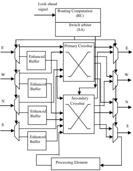
[image:3.595.364.483.128.249.2] [image:3.595.100.229.156.358.2] [image:3.595.82.235.380.582.2] [image:3.595.103.221.608.733.2]At low load condition the all packets would only traverse the primary crossbar and follow minimum path and experiences minimum delay so behave as bufferless network. At high load the packets get traverse from secondary cross bar through a enhanced buffer which provides a function of hand shaking by providing a ready valid handshake signal. In the Figure 5 proposed router with enhanced buffer is shown. It is having four input port at low traffic the data flit traverse though primary switch at heavy load the flit get store in the enhanced buffer and the data flit traverse through secondary crossbar. The function of processing element is to give feedback from output to input to show whether the flit is valid or not. Buffers are provided in front of secondary in which the data moves serially as the virtual channel is eliminated so the virtual allocator stage is eliminated. Switch arbiter (SA) is modified to make control over the Demux and Mux to maintain the correct packet flow in both crossbars. The elimination of VCs eliminates the VA stage and simplifies SA stage, so that SA and ST could be performed in the same cycle the number of stages reduce to 3 so shown in Figure 6(c).
(a) (b) (c)
The function of enhanced buffers is a flow-control scheme that uses the storage already present in pipelined channels in place of explicit input VCBs. With this approach, the channels themselves act as distributed FIFO buffers under congestion. Without VCBs, and hence VCs, deadlock prevention is achieved by duplicating physical channels. Duplicate physical channels must be used in the same way as VCs to prevent deadlocks and to differentiate between traffic classes. Figure 7(a) shows a Dflip-flop (DFF) that is implemented using master and slave latches. By adding control logic to drive the latch enable pins independently, each latch can be used as an independent storage location. Thus, the FF becomes an EB, a FIFO with two storage locations. This is illustrated in Figure 7(b).
EB use ready(R) and valid (V) handshake to advance data. Output of ready indicates that enhanced buffer has at least one empty storage slot to latch more data. Valid outputs indicate that the data currently being driven is valid. The control logic samples incoming control signals at rising clock edges to determine if data has advanced to or from theEnhanced buffer. Asserted ready and valid signals between two EBs indicate that data has advanced. Data is latched in the master latch at the end of the cycle, and advances to the slave at the beginning of the next cycle. . If during the previous cycle the incoming ready was de-asserted and the state remains at 1, data is already in the slave latch and its enable input needs to be disabled .In the buffered secondary crossbar the incoming
flits are stored at the selected cross point for their output. At the second stage, outputs arbitrate among all the valid cross points and store flits into the output. The ready-valid handshake is used
Figure: 7 (a) A DFF with master and slave D latch Data D Q
Master Latch EN
D Q Slave Latch EN
Clk Routing Computation
(RC)
Switch arbiter (SA) Look ahead
signal
Primary Crossbar
Enhanced Buffer
Enhanced Buffer
Enhanced Buffer
Enhanced Buffer
Processing Element E
W
N
S
E
W
N
S Secondary
Crossbar
Figure 6: (a) 6 stage generic router (b) 5 stage ViChaR router(c) 3 stage proposed router with enhanced buffer
V_in
R_out Enhanced Buffer
D Q Master Latch
EN
D Q Slave Latch EN
EB Control Logic
V_out
R_in
[image:4.595.59.291.73.371.2]ENM ENS
Figure: 5-Proposed router with enhanced buffer
Figure 7 (b): A EB is a FF whose latch are control by the EB control logic
BW
RC
VA
SA
ST
LT BW
RC
VA
SA
ST
LT
BW
RC
SA
ST
[image:4.595.314.501.248.370.2] [image:4.595.319.517.547.695.2] [image:4.595.105.243.605.737.2]in both stages. The comparison of three techniques is shown in the Table 1 based on the parameters.
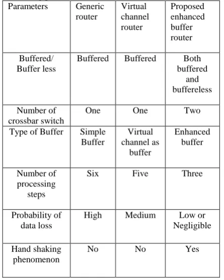
Table 1: Comparison of proposed router with other on the basis of following parameters
Parameters Generic
router
Virtual channel router
Proposed enhanced buffer router
Buffered/ Buffer less
Buffered Buffered Both
buffered and buffereless
Number of crossbar switch
One One Two
Type of Buffer Simple
Buffer
Virtual channel as
buffer
Enhanced buffer
Number of processing
steps
Six Five Three
Probability of data loss
High Medium Low or
Negligible
Hand shaking phenomenon
No No Yes
As shown in the Table 1 we can see that the advantage of both buffer as well as bufferless is achieved. Enhanced buffer is used which is based on control logic. The number of processing step is reduced to three as the virtual channel allocator (VA) is removed. The probability of data loss is low or negligible as it works on the concept of handshaking which works on the availability of valid or ready signal till the no flit is transmit or received. Based on the above parameter proposed enhanced buffer router give better performance compare to other techniques.
4.
IMPLEMENTATION AND RESULTS
Implementation is done in cadence virtuoso at 180nm .The designing parameter are selected at the time of designing. Generic router and virtual channel router are design for making comparative study between the three techniques.Table 2 shows the comparison based on the delay and total average power.
Table 2: Comparison with the existing techniques
Design Delay(nsec) Total average
power(μW)
Generic router 41.39 527.7
Virtual channel router
0.877 445.1
Proposed enhanced buffer router
0.358 427.5
The delay and average power of generic router is maximum, which are significantly reduced using virtual channel router. In proposed design both the quantities reduced further as we can also see in Figure 8 and Figure 9.
[image:5.595.56.279.119.398.2]
Figure 8: Delay in different routers
Figure 9: Total average power in different routers
Table 3 shows the percentage reduction of delay and power of virtual channel and proposed router in terms of delay and power. The virtual channel routerresults 97.8811% reduction in delay and 15.6528% saving in average power as compared to generic router. The proposed enhanced buffer router performs better then virtual channel router in both the parameters. it diminishes the delay by 99.1350% and average power by 18.9881% as that of generic router. Figure 10 shows the circuit diagram of proposed enhanced buffer Router. Figure 11 show the delay of proposed enhanced buffer Router. Figure 12 show the power of proposed enhanced buffer Router.
0 5 10 15 20 25 30 35 40 45
Generic router
Virtual channel
router
Proposed enhanced buffer router
41.39
0.877 0.358
Delay(nsec)
0 100 200 300 400 500 600
Generic router Virtual
channel router
Proposed enhanced buffer router 527.7
445.1 427.5
[image:5.595.308.537.130.315.2] [image:5.595.308.533.348.535.2]Table3: Percentage change reduction with generic router
Design
% change in Delay w.r.t. generic router
% change in Total average power w.r.t. generic router
Virtual
channel router 97.8811 15.6528
Proposed enhanced buffer router
[image:6.595.55.291.423.580.2]99.1350 18.9881
[image:6.595.54.291.598.748.2]Figure 10: Proposed enhanced buffer Router Circuit
Figure 11: Delay of proposed enhanced buffer Router
Figure 12: Power of proposed enhanced buffer Router
5.
CONCLUSION
In proposed design the advantage of both buffered and bufferless is achieved. At low load condition the packet traversal is done through a bufferless network and at high load the packet traversal is through enhanced buffer ie buffered network. It provides better results than generic NoC router as well as virtual channel router. Proposed router achieves 18.98% power saving compared to generic router and 15.6% compare to virtual channel router. In terms of delay the proposed router provided 99.13% less delay than generic router and 97.88% less delay as compared to virtual channel router. Reducing pipeline stages result in reduced delay for packets in each router, which in turn decreases the average latency. Because packets spend less time traveling in the network, the now-unoccupied cycles enable more packets to be transmitted and increase the throughput of the network.
6. REFERENCES
[1] L. Benini and G. De Micheli, “Networks on chips: A new SoC paradigm,”Computer, vol. 35, no. 1, pp. 70–78, 2002. [2] W. J. Dally and B. Towles, “Route packets, not wires:
On-chip interconnection networks,” in DAC ’01: Proceedings of the 38th Conference on Design Automation, Jun. 2001, pp. 684–689.
[3] P. Guerrier and A. Greiner, “A generic architecture for on-chip packet-switched interconnections,” in DATE ’00: Proceedings of the Conference on Design, Automation and Test in Europe, Mar. 2000, pp. 250–256.
[4] Z. Lu and A. Jantsch, “Flit ejection in on-chip wormhole-switched Networks with virtual channels,” in NORCHIP ’04: Proceedings of the 2004 IEEE/ACM International Conference on Norchip, Nov. 2004, pp. 273–276.
[5] J. Hu, ¨ U. Y. Ogras, and R. Marculescu, “System-level buffer allocation for application-specific networks-on-chip router design,” IEEE Trans. on CAD of Integrated Circuits and Systems, vol. 25, no. 12, pp. 2919–2933, Jan. 2006. [6] Z. Lu and A. Jantsch, “Flit ejection in on-chip
wormhole-switched Networks with virtual channels,” in NORCHIP ’04: Proceedingsof the 2004 IEEE/ACM International Conference on Norchip, Nov. 2004, pp. 273–276.
[7] C. A. Nicopoulos, D. Park, J. Kim, N. Vijaykrishnan, M. S. Yousif, and C. R. Das,“ViChaR: A dynamic virtual channel regulator for network-on-chip routers,” in MICRO’39: Proceedings of the 39th Annual IEEE/ACM International Sympo-sium on Microarchitecture, Dec. 2006, pp. 333–346.
[8] L. S. Peh, W. J. Dally, and P. Li-Shiuan, “Delay model for router microarchitectures,” IEEE Micro, vol. 21, no. 1, pp. 26–34, 2001.
[9] T. Moscibroda, O. Mutlu, ‘‘A case for bufferless routing in on-chip networks, in Proceedings of the 36th Annual International Symposium on Computer Architecture, June 2007.
[10]S. Borkar, “Design challenges of technology scaling,” IEEE Micro, vol. 19, pp. 23–29, 1999
[11]S. Ramany and D. Eager, “The interaction between virtual channel flow control and adaptive routing in wormhole networks,” in ICS ’94: Proceedings of the 8th
[12]Y. Hoskote, S. Vangal, A. Singe, N. Borkar, and S. Borkar, “A 5-ghz mesh interconnect for a teraflops processor,” IEEE Micro, vol. 27, no. 5, 2007.
[13]H. Wang, L.-S. Peh, and S. Malik, “Power-driven design of router
[14]Microarchitectures in on-chip networks,” in MICRO 36: Proceedings of the 36th annual IEEE/ACM International Symposium on Microarchitecture. Washington, DC, USA: IEEE Computer Society, 2003, p. 105.
[15]S. Kim, M. B. Taylor, J. Miller, and D. Wentzlaff, “Energy characterization of a tiled architecture processor with
on-chip networks,” in ISLPED ’03: Proceedings of the 2003 international symposium on Low power electronics and design. New York, NY, USA: ACM, 2003, pp. 424–427. [16]A. K. Kodi, A. Sarathy, and A. Louri, “ideal: Inter-router
dual-function energy- and area-efficient links for network-on-chip (noc),” in Proceedings of the 35th International Symposium on Computer Architecture.(ISCA’08), Beijing, China, June 2008, pp. 241–250.