N A N O E X P R E S S
Open Access
Morphological, compositional, structural, and
optical properties of Si-nc embedded in SiO
x
films
J Alberto Luna López
1*, J Carrillo López
1, D E Vázquez Valerdi
1, G García Salgado
1, T Díaz-Becerril
1,
A Ponce Pedraza
2and F J Flores Gracia
1Abstract
Structural, compositional, morphological, and optical properties of silicon nanocrystal (Si-nc) embedded in a matrix of non-stoichiometric silicon oxide (SiOx) films were studied. SiOxfilms were prepared by hot filament chemical vapor deposition technique in the 900 to 1,400°C range. Different microscopic and spectroscopic characterization techniques were used. The film composition changes with the growth temperature as Fourier transform infrared spectroscopy, energy dispersive X-ray spectroscopy, and X-ray photoelectron spectroscopy reveal. High-resolution transmission electron microscopy supports the existence of Si-ncs with a diameter from 1 to 6.5 nm in the matrix of SiOxfilms. The films emit in a wide photoluminescent spectrum, and the maximum peak emission shows a blueshift as the growth temperature decreases. On the other hand, transmittance spectra showed a wavelength shift of the absorption border, indicating an increase in the energy optical bandgap, when the growth temperature decreases. A relationship between composition, Si-nc size, energy bandgap, PL, and surface morphology was obtained. According to these results, we have analyzed the dependence of PL on the composition, structure, and morphology of the Si-ncs embedded in a matrix of non-stoichiometric SiOxfilms.
Keywords:Silicon nanocrystals, High-resolution TEM, XRD, PL, AFM, HFCVD PACS:61.05.-a, 68.37.Og, 61.05.cp, 78.55.-m, 68.37.Ps, 81.15.Gh
Background
Since the discovery of light emission from porous silicon [1], an intense investigation of materials compatible with silicon technology with excellent optical properties has been under development. Recently, materials containing silicon nanocrystal (Si-nc) have attracted the interest of researchers due to their optical properties. Therefore, a great variety of materials with these characteristics have been studied [2-5]. One of these materials is the non-stoichiometric silicon oxide (SiOx); this material contains Si excess agglomerates to create Si nanoparticles embedded in an oxide matrix. SiOx shows some special compos-itional, structural, morphological, and optical properties that vary with the Si excess. In particular, the optical char-acteristics of SiOxfilms can be varied with the growth tem-peratures. For example, refractive index varies from 1.6 to 2.4 when the growth temperature is changed; also, SiOx
emits visible light. These characteristics have given place to various types of applications such as waveguides, no vola-tile memories, light radiation, and detection devices [6-8]. Furthermore, the fabrication of SiOx films is completely compatible with complementary metal oxide semicon-ductor technology, providing an easy way for the optoelec-tronic integration on silicon. Several techniques have been employed to make thin SiOx films, such as high-dose Si ion implantation into SiO2films [6,9], low pressure chem-ical vapor deposition [8], sol–gel, hot filament chemical vapor deposition (HFCVD) [10,11], and plasma enhanced chemical vapor deposition [12], in which an improvement of the optical and structural properties as the PL emission and Si excess has been reported. In this work, HFCVD technique was used to deposit SiOx films on silicon and quartz substrates. This technique allows us to obtain thin SiOx films with different properties just by varying the source-substrate distance during the deposit; this distance changes the growth temperature. Structural, compositional, morphological, and optical properties of SiOx films pre-pared by HFCVD and an analysis of the composition,
* Correspondence:[email protected]
1
IC-CIDS Benemérita Universidad Autónoma de Puebla, Ed. 103 C o D, Col. San Manuel, C.P, Puebla, Pue 72570, Mexico
Full list of author information is available at the end of the article
morphology, Si-nc size, and their relation with the PL emission are presented.
Methods
Si-ncs embedded in thin SiOx films were deposited on quartz and n-type silicon (100) substrates, the silicon sub-strates with 2,000- to 5,000-Ωcm resistivity in a horizontal hot filament CVD reactor using quartz and porous silicon as the sources. A hot filament at approximately 2,000°C dissociates ultra-high purity molecular hydrogen which flows into the reactor at a 50 sccm rate and produces atomic hydrogen (H). Something worth mentioning in this process is the use of a hydrogen flux on top of the hot fila-ment, which resulted in a remarkable improvement of the optical and structural properties of the SiOx films depos-ited. The substrates were carefully cleaned with a metal oxide semiconductor standard cleaning process, and the native oxide was removed with an HF buffer solution be-fore being introduced into the reactor. The heating rate depends on the source-substrate distance (dss). The react-ive species (H) forms a volatile precursor (SiO) deposited on the silicon substrate and produces Si-ncs embedded in thin SiOx films. The filament-source distance was kept constant (2 mm). The relationship between the filament temperature (approximately 2,000°C) and the variation of the dss of 2, 3, 4, 5, and 6 mm provides a change in the growth temperature (Tg) of 1,400°C, 1,300°C, 1,150°C, 1,050°C, and 900°C, which was measured with a thermo-couple in each position, respectively. These changes in the dss and Tg, consequently, have modified the silicon excess and defects in the non-stoichiometric SiOxfilms. The film refractive index and the film thickness were measured using a null Ellipsometer Gaertner L117 (Gaertner Scien-tific Co., Chicago, IL, USA) with a laser of He-Ne (632.8 nm); the film thickness was measured using a Dek-tak 150 profilometer (Veeco Instruments Inc., Plainview, NY, USA). FTIR spectroscopy measurements were done using a Bruker system model vector 22 (Bruker Instru-ments, Bellirica, MA, USA). XPS analysis was carried out using a Thermo Fisher spectrometer (Thermo Fisher Scientific, Waltham, MA, USA) with a monochromatic Al radiation XR15 and energy of 15 eV. PL response was mea-sured at room temperature using a Horiba Jobin Yvon spectrometer model FluroMax 3 (Edison, NJ, USA) with a pulsed xenon source whose detector has a multiplier tube, which is controlled by computer. The samples were excited using a 250-nm radiation, and the PL response was recorded between 400 and 900 nm with a resolution of 1 nm. Room-temperature transmittance of the SiOx films was measured using a UV–vis-NIR Cary 5000 system (Agi-lent Technologies Inc., Santa Clara, CA, USA). The trans-mittance signal was collected from 190 to 1,000 nm with a resolution of 0.5 nm. HRTEM measurements and XEDS were done using a Titan 80- to 300-kV model with an
energy spread of 0.8 eV. HRTEM micrographs were ana-lyzed using Gatan DigitalMicrograph software (Gatan Inc. Pleasanton, CA, USA) [13]. The surface morphology of non-stoichiometric SiOxfilms was studied using a scanning probe microscopy of Ambios Technology (Santa Cruz, CA, USA), operated in non-contact mode. A 4 × 4-μm2scanned area was used for each topographic image, and a 460-μ m-long single-crystal Si n-type cantilever operated at 12 kHz (type MikroMash SPM Probes (San Jose, CA, USA)) was used. Four different scans were done for each sample, showing good reproducibility. AFM images were analyzed using scanning probe image processor software [14].
Results and discussion
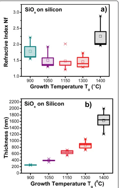
[image:2.595.307.540.336.703.2]The refractive index and thickness of the SiOx films as a function of the growth temperature are shown in Figure 1; the refractive index of the thin SiOxfilms changes with Tg. Thicker samples were obtained when the growth temperature was increased from 900°C to 1,400°C. A
Figure 1Refractive index (a) and thickness (b) as functions of growth temperature of the SiOxfilms.
variation in the refractive index from 1.4 to 2.2 was measured when the growth temperature was increased from 1,150°C to 1,400°C. This variation has been related to a change of the silicon excess in SiOxfilms [12]. Therefore, we can modify the silicon excess in the SiOx films by changing the growth temperature.
FTIR absorption spectra of thin SiOxfilms are shown in Figure 2. These spectra show the absorption peaks asso-ciated with the rocking (458 cm−1) (peak 1), bending (812 cm−1) (peak 2), on-phase stretching (1,084 cm−1) (peak 4), and out-of-phase stretching (1,150 cm−1) (peak 5) vibration modes of the Si-O-Si bonds in SiO2 [7,15,16]. The position of the stretching absorption peak in SiOx films changes with the growth temperature. Tg produces changes only with regard to the microstructure of the films, where the radiative defects can be activated during the process. The on-phase stretching peak position slightly moves towards a higher wavenumber with a higher growth temperature. On the other hand, the out-of-phase stretch-ing peak position shows similar changes with the growth temperature. The position of peak (4) depends on silicon
[image:3.595.304.539.88.295.2]excess. This is an evidence that the SiOxfilms have a great content of sub-stoichiometric SiOx (x< 2) phase in the as-deposited state. Peaks in the spectra at 883 cm−1(peak 3), corresponding to Si-H bending and Si-OH, and the other one located at 2,257 cm−1(peak 6), corresponding to Si-H stretching, are observed [17-19]; these bonds are present in the films due to hydrogen incorporation during the growth process. Also, a peak centered at 2,352 cm−1 (peak 7) comes from the CO2content in the atmosphere [20]. Furthermore, the peak intensity changes with the growth temperature as shown in Figure 2. A relation between peak intensity and thickness is established; to bigger peak intensity, a bigger thickness. In Figure 1, we can see that if there is a high growth temperature then the thickness increases. Therefore, the peak intensity is bigger too. Moreover, the oxygen and hydrogen contents change with the growth temperature. The hydrogen and oxygen contents decrease when the growth temperature increases, as can be seen with the behavior of the peaks 3 and 7 and peaks 2, 4, and 5, respectively, as shown in Figure 2. Figure 2FTIR absorption spectra of the thin SiOxfilms for
[image:3.595.58.288.88.273.2]different growth temperature.The numbers (1 to 7) mean different vibration modes, which are described in Table 1.
Table 1 Compositional results (atomic percentages of oxygen (O) and silicon (Si))
Temperature (°C) dss (mm) Atomic percentage x= O/Si
O Si
1,400 2 30.76 69.22 0.44
1,300 3 61.60 38.38 1.60
1,150 4 56.02 43.96 1.27
1,050 5 64.48 35.50 1.81
900 6 62.49 37.50 1.66
Results of the SiOxfilms obtained by XEDS.
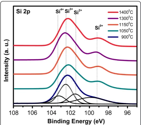
[image:3.595.307.538.623.732.2]Figure 3Si 2p XPS spectra show the composition of the SiOx films.
Table 2 Oxidation states of the SiOxfilms obtained by means of the convolution of the XPS curves
Oxidation states Temperature (°C) dss (mm) Peak position (eV)
Si0+ Si2+ Si3+ Si4+
1,400 2 99.08 101.06 102.16 102.95
1,300 3 99.67 101.98 103.01
1,150 4 99.08 101.47 102.51 103.24
1,050 5 99.02 101.32 102.28 103.16
[image:3.595.56.291.629.725.2]XEDS spectra of the SiOxfilms were realized for several growth temperatures; the stoichiometric ratio is determined by the atomic percentages of silicon and oxygen. The peak intensities of oxygen and silicon change with the growth temperature. The peak intensities of silicon are higher when decreasing the growth temperature, and the peak intensities of oxygen decrease when increasing the growth temper-ature. These variations indicated that the stoichiometry of the SiOx films changes with the growth temperature. We can see that the oxygen content decreases with the increase of the growth temperature, and the silicon content decreases with the increase of the growth temperature. Then, with higher growth temperature, the silicon content increases and the oxygen content decreases. In Table 1, the composition results of the XEDS spectra are listed. Figure 3 shows the XPS experimental spectra of the Si 2p line and the evolution of the Si 2p line of different SiOxfilms. The four oxidation states, as well as the unoxidized state, can be modeled as tetrahedral bonding units, in which a central Si atom is bonded to (4−n) Si atoms and n oxygen atoms (Si-Si4−nOn) withn= 0 to 4. Therefore, the 99.5 eV peak is associated with elemental silicon. SiO2spectra increase the peak energy to 103.3 eV, corresponding ton= 4. The Si 2p binding energies are normally about 99 to 103 eV. It is widely accepted that the Si 2p photoelectron peak of SiOx contains five components, corresponding to a non-oxidized state and four different oxidation states of Si [21,22]. The variation of the oxidation states of the SiOx films leads to peak position’s shift, as shown in Table 2. A peak at about 99 eV accompanied by a peak at about 103 eV is present; they can be attributed to Si and SiO2, respectively, and any variation could be attributed to sub-oxidized silicon [23,24]. The increasing electro-negativity of the Si-O bound relative to the Si-Si bond results in a shift to a higher binding energy of the core level electrons in the silicon.
AFM images of the SiOxfilms in Figure 4 are presented. All images exhibit a rough surface. It can be seen that the
surface exhibits different characteristics depending on the growth temperature, which influences the size of the grains (roughness), their form, and composition. Average rough-ness decreases by decreasing the Tg and thickrough-ness [8]. The roughness analysis is shown in Figure 5. It is observed that the surface roughness of SiOx films with lower Tg is less than that with higher Tg, except for Tg = 1,150°C. The high roughness of the sample grown at 1,400°C is probably the cause of the index variation with a not clear tendency, and the roughness could be due to the big nanocrystals embed-ded in the SiOxfilms.
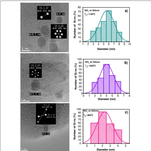
On the other hand, the structure of SiOx films was analyzed using the HRTEM technique. Figure 6 shows the HRTEM images for the SiOx films, which indicate the presence of Si-ncs embedded in the SiOx films. Some of them are semi-elliptical, and some other ones have an enlarged shape. The agglomeration process takes place between the nearest Si-nanoclusters forming Si-nc. All micrographs show that the SiOx matrix contains small a) SiOx films deposited on silicon. Grown Temperature (Tg)
[image:4.595.60.540.90.245.2]Tg = 1400 C Tg = 900 C
Figure 43D AFM images of SiOxfilms deposited on silicon substrate at different Tg.Scanned area is 4 × 4μm2.
Figure 5Average roughness (Sa) as a function of Tg for SiOx films.Scanned area is 4 × 4μm2.
[image:4.595.306.539.519.703.2]clusters, which on the basis of the selected area electron diffraction (SAED) analysis can be identified as Si-nc. SAED is referred to as ‘selected’ because, in the micro-graph, it can easily choose which part of the sample we obtain the diffraction pattern; in our case, only on the Si-nc. About ten micrographs were obtained to each sample; with them, a statistical analysis of the distribu-tion of the Si-nc diameter sizes was realized. A great dispersion of diameter sizes is observed; the diameter size goes from 1 up to 9 nm, being the average diameter
size around 5.5, 4, and 2.5 nm for 1,150°C, 1,050°C, and 900°C, respectively, as indicated in the histograms of Figure 6a,b,c.
From AFM images, the samples grown with lower Tg look more homogeneous than those grown with higher Tg. As shown in the HRTEM images, the silicon excess agglomerates to create Si-ncs; then, the roughness observed in AFM measurements can be associated with Si-ncs and compounds. In addition, FTIR spectra show a phase separation (Si and SiO2), which is
1 2 3 4 5 6 7 8 9 10
0 10 20 30 40 50 60 70 80
a
)
SiOx on SiliconTg= 11500
C
Number of Si-nc (%)
Diameter (nm)
0 1 2 3 4 5 6 7 8
0 10 20 30 40 50 60 70 80 90 100
b
)
SiOx on SiliconTg= 10500
C
Number of Si-nc (%)
Diameter (nm)
0 1 2 3 4 5
0 10 20 30 40 50 60 70 80 90 100
Diameter (nm)
Nu
mber of Si-nc (%)
SiOx on Silicion
Tg= 9000
C
[image:5.595.56.538.88.571.2]c
)
deduced from the shift of the Si-O stretching vibration mode towards the SiO2 frequency value, and it is corroborated with both XPS and HRTEM. Therefore, elemental Si, SiOx, and SiO2 phases with Tg are present, and depending on Si excess, the roughness, size of Si-nc, oxidation states, and vibration modes of the Si-O-Si bonds, some of these phases could be dom-inant. This indicates that a direct correlation between the roughness, size of Si-nc, oxidation states, and vibration modes of the Si-O-Si bonds exists. In other words, the roughness is produced by the formation of Si-ncs and oxidation states. The diffusion of excess silicon at high Tg produces Si-ncs in the SiOx films, i.e., the silicon particles diffuse to create silicon agglomerates around the nucleation sites when the SiOxis grown at high Tg.
Figure 7 shows the PL response of SiOxfilms correspond-ing to different growth temperatures. At all samples, a wide PL spectrum is observed. At the growth temperatures of 1,150°C, 1,050°C, and 900°C, the PL peaks are at 558, 546, and 534 nm, respectively. At the highest growth temperature (1,400°C), the PL has the weakest intensity, and the PL peak has the longest wavelength of 678 nm. Moreover, the PL bandwidth and intensity increase for growth temperatures lower than 1,400°C. Therefore, the PL also depends on Tg, size of Si-nc, roughness, oxidation states, and vibration modes of the Si-O-Si bonds, as shown previously.
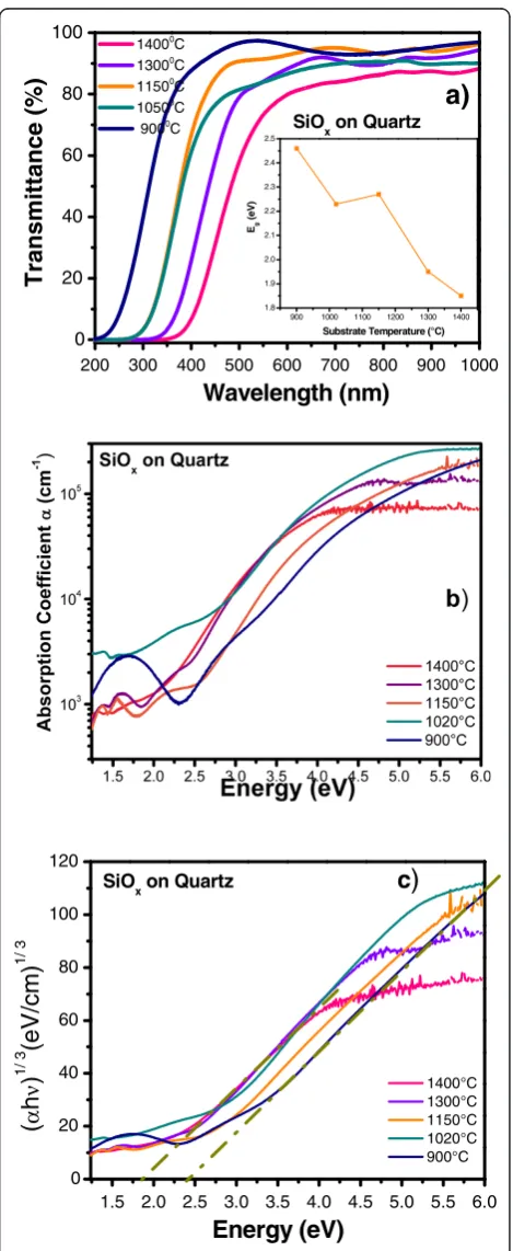
[image:6.595.305.540.96.668.2]The optical bandgap of SiOxfilms is obtained with trans-mittance spectra measurements. Transtrans-mittance spectra for SiOxfilms deposited on quartz are shown in Figure 8a. The transmittance of all these films is relatively high (>80%) between 600 and 1,000 nm, as shown in the figure, and reduces to zero for wavelengths below 600 nm. The grow-ing temperature produces a clear change of the curves and
Figure 7PL spectra of the SiOxfilms with different Tg.Inset shows the convolution realized to PL spectra.
200 300 400 500 600 700 800 900 1000
0 20 40 60 80 100
a)
900 1000 1100 1200 1300 1400 1.8
1.9 2.0 2.1 2.2 2.3 2.4 2.5
Eg
(e
V
)
Substrate Temperature (°C)
14000C
13000C
11500C
10500C
9000C
Transmi
ttance (%)
SiOx on Quartz
Wavelength (nm)
1.5 2.0 2.5 3.0 3.5 4.0 4.5 5.0 5.5 6.0
0 20 40 60 80 100 120
SiOx on Quartz
(
α
h
ν
)
1/ 3
(eV/cm)
1/ 3
Energy (eV)
1400°C 1300°C 1150°C 1020°C 900°C
c
)
Figure 8UV–vis transmittance spectra, absorption coefficient versus energy, and (αhν)1/3versus energy (hν).(a) UV–vis
transmittance spectra and the inset show the energy optical bandgap from SiOxfilms as a function of growth temperature, (b) absorption coefficient versus energy, and (c) (αhν)1/3versus energy (hν). The dashed lines show the linear fit of the straight part.
[image:6.595.57.292.524.702.2]a shift towards lower wavelengths related to a silicon excess change of the SiOx films [11,25,26]. In Tauc’s plot, an increase in the energy bandgap (Eg) has been detected when the growth temperature decreases, as shown in the inset of Figure 8a. The values of the optical bandgap Eg can be estimated from the following equation known as the Tauc plot [27,28]:
αhv¼A hvEg
n ;
whereEgis the optical bandgap corresponding to a particu-lar transition in the film;A, a constant;ν, the transmission frequency, which multiplied by the plank constant h we have photon energy hv, and the exponent n characterizes the nature of band transition. The absorption coefficients α(λ) were determined from transmission spectra with the following relation:
α λð Þ ¼ln½Tð Þλ
d ;
whereT(λ) is the transmittance, and d is the thickness of the SiOxfilms.αversushvis shown in Figure 8b. On the other hand, values ofn= 1/2 and 3/2 correspond to direct-allowed and direct-forbidden transitions; n= 2 and 3 are related to indirect-allowed and indirect-forbidden transi-tions, respectively [28]. From a plot (αhν)1/nversushν, the bandgap can be extrapolated from a straight line tohν= 0. For all different growth temperatures, the best straight line is observed for n= 3 (Figure 8c), indicating an indirect-forbidden transition mechanism.
The optical properties such as the energy bandgap and the PL bands between (400 to 700 nm) are usually some of the important characteristics of these materials. The PL of SiOx films has been extensively studied in the literature [1-25]. Two major mechanisms for PL in this kind of materials are generally accepted: quantum confinement effects in the Si-ncs and defect-related effects, as defects at the Si/SiOx interface and defects associated with oxygen vacancies in the film. The first mechanism of light emission that we can consider in the SiOx material is related to some kinds of defects pro-duced during the growth process, as shown in the EDS, XPS, and FTIR spectra, where we have bonding such as neutral charged oxygen vacancies (NOV) (Si-Si bonds), non-bridging oxygen hole center (NBOHC), positively charged oxygen vacancies (E’centers), interstitial oxygen molecules and peroxide radicals [13,14,23,29,30], which can form Si-nps or E’centers. Therefore, the increase of PL with the Tg is due to the activation of some of these radiative defects. In this study, the 550-nm PL band has been associated with silicon excess in the film in the NOV defects and E’ centers [2,26] types. These bands appear well defined only if the film has been grown with temperatures within 900°C and 1,150°C. If the film was
grown at a higher temperature, the band at 700 nm appears with its maximum PL emission.
On the other hand, as a second mechanism of emis-sion, the luminescence peak of SiOxfilms shows a blue-shift when the Tg decreases; this behavior is ascribed to quantum confinement effect in the Si-nc. Therefore, in this case the PL spectra are analyzed in terms of a quantum confinement model [1,22]:
ENð Þ ¼eV 1;240=λðnmÞ
ENð Þ ¼eV 1:12eVþ 3:73=d1:39
⇒dðnmÞ ¼ 3:73 EN1:12
1
1:39
;
ð1Þ
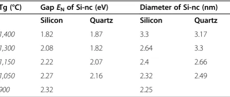
which corresponds to the radiative recombination of electron–hole pairs in the Si-nc, wheredand ENare the diameter and energy of the Si-nc, respectively, and λ (nm) is the wavelength of the Si-nc emission. Table 3 shows the theoretical values of average size of Si-nc calculated from the PL spectra, where the size of the Si-nc reduces and the energy band gap increases with decreasing the growth temperature, similar to an effect of quantum confinement. Note that unlike as stated in the literature for the quantum confinement effect, PL spectra are very wide which indicates that two possible mechanisms are involved.
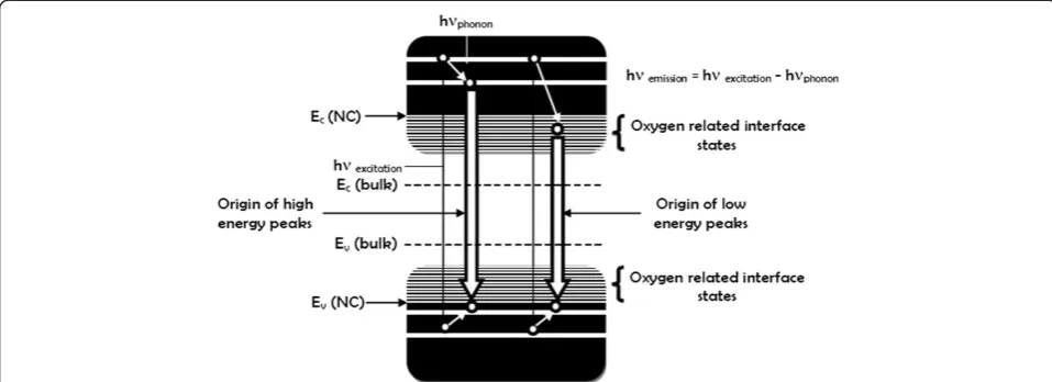
[image:7.595.306.538.618.716.2]Why is it possible that two mechanisms be involved? When a deconvolution to the PL spectra is made, as shown in the inset of Figure 7, different peaks are defined; some of them are related to different kinds of defects, as listed in Table 4. Therefore, the high-energy PL peaks are associated with quantum confinement effects in Si-ncs, while the low-energy PL peaks are associated with defects. Such a behavior is described in the schematic diagram of the band structure (Figure 9); a similar behavior has been reported previously [31]. This diagram represents the radiative tran-sition giving rise to the emission peaks. For the more energy occurs the generation of electron–hole pairs within the Si-nc core, followed by a thermal relaxation within the conduction band of the Si-nc which in turn suggests the recombination of carriers. In the case of the less energy
Table 3 Theoretical values
Tg (°C) GapENof Si-nc (eV) Diameter of Si-nc (nm)
Silicon Quartz Silicon Quartz
1,400 1.82 1.87 3.3 3.17
1,300 2.08 1.82 2.64 3.3
1,150 2.22 2.07 2.4 2.66
1,050 2.27 2.16 2.32 2.49
900 2.32 2.25
Values of theENand diameter of the Si-nc calculated from the PL spectra as a
peaks, phonon relaxation involves more energy because of the transitions between the states of interfacial defects.
The existence of Si-ncs in the SiOx films was corrobo-rated with the HRTEM measurements. The diffusion of Si excess due to the deposit at high temperature, i.e., when the SiOx films are being deposited, could produce Si-ncs. The silicon particles diffuse themselves to create silicon agglom-erates around the nucleation sites. If the Si excess is high enough, the Si agglomerates will be crystallized to form Si-ncs. A decrease in the Si-nc diameter has been detected when the growth temperature reduces. The high growth temperature induces the formation of crystals as the statis-tical analysis of the crystal size distribution, obtained from the HRTEM images, shown. Therefore, the mean diameter of Si-ncs depends on the growth temperature.
Then, two transition mechanisms are possible as the above results and discussion showed widespread bandgap transitions induced by quantum confinement and interface state transitions associated with defects in the oxide. The widespread transitions in Si-nc may bring about high energy peaks (blueshifted PL peaks), and if this energy decays between defects (NOV, NBOHC, and E’ center-related interface states), it can give place to low energy
peaks (redshifted PL peaks). All these data indicate that light emission from the films is due to the Si-ncs embedded in the amorphous SiOxmatrix and defects. Accordingly, we have proposed a combination of mechanisms to explain the photoluminescence in the films.
Conclusions
[image:8.595.56.541.112.225.2]SiOx films deposited by HFCVD at different growth temperatures were analyzed. These films exhibit an intense PL with a main peak at 550 nm. The strongest PL was obtained for SiOx films deposited at 1,150°C. Ellipsometry, XEDS, XPS, FTIR, AFM, PL, transmit-tance, and HRTEM techniques were used to obtain the structural, compositional, and optical properties of the SiOx films, and they were studied as a function of the growth temperature. Thicker samples were obtained when the growth temperature was increased from 900° C to 1,400°C. A variation in the refractive index from 1.4 to 2.2 was obtained when the growth temperature was increased from 1,150°C to 1,400°C. From AFM images, the samples grown with the lower growth tem-peratures look more homogeneous than those grown with the higher Tg. As shown in the HRTEM images, Table 4 Peak position obtained by deconvolution from PL spectra and defect types relationated with the peak
position
Defect types Peak positions (nm) Reference
1,400°C 1,300°C 1,150°C 1,050°C 900°C
NOV defects (O3≡Si-Si≡O3) 428 483 458 467 [12]
Centers of defects E’δ 521 523 [12]
E’δcenter or oxygen deficiency 553 559 [12,32]
Defect vacancies of oxygen (O≡Si-Si≡O) 591 600 579 584 [30,33]
Oxide relationated in the interface of Si/SiOx 675 695 [31,34]
Not identified 796 813
Figure 9Schematic representation of the band structure and mechanisms responsible for PL from SiOxfilms.
[image:8.595.57.536.539.713.2]the silicon excess agglomerates to create Si-ncs; in this way, the roughness observed through AFM measure-ments can be associated with Si-ncs and compounds. In addition, FTIR spectra show a phase separation (Si and SiO2), which is deduced by the shift of the Si-O stretching vibration mode towards the SiO2frequency value, which is corroborated with XPS and HRTEM. A clear relation between the surface roughness, size of Si-nc, oxidation states, composition, and the PL prop-erty was obtained. Therefore, PL depends strongly on the Tg and properties of the SiOxfilms.
Competing interests
The authors declare that they have no competing interests.
Authors’contributions
JALL and DEVV participated in the growth of the films, carried out the FTIR, PL, and UV measurements and drafted the manuscript. JCL conducted the ellipsometry and AFM measurements. GGS and TDB conducted the SiOx growth. APP conducted the HRTEM and XEDS measurements. FJFG coordinated the study. JALL provided the idea and supervised the study. All authors read and approved the final manuscript.
Authors’information
JALL is currently a researcher and professor in the Science Institute - Center of Investigation in Semiconductors Devices (IC-CIDS) from Autonomous University of Puebla, Mexico. He started to work on electrical and optical characterization of the MOS structures. His research interest is the physics and technology of materials and silicon devices. Moreover, his research interests are, too, the nanotechnology, material characterization, and optoelectronic devices such as sensor, LEDs, and solar cells.
GGS received his PhD in the Electronic and Solid State Department from the Center of Research and Advanced Studies, National Polytechnic Institute, Mexico City in 2003. He started to work on the growth and characterization of non-stoichiometric silicon oxide. His current research interests include metallic oxides obtained by the HFCVD technique, GaN obtained by the metal organic CVD technique and porous silicon gas sensor devices. FJFG is a coordinator and researcher at the Posgrado en Dispositivos Semiconductores in Benemérita Universidad Autónoma de Puebla, México and was a participant in many important international conferences. Professor FJFG has published many journal articles. His research interests include experiments and models in photoluminescence and quantum confinement in off stoichiometry silicon oxides.
Acknowledgments
This work has been partially supported by CONACyT-154725 and VIEP-BUAP-2012. The authors acknowledge INAOE and CIQA laboratories for their help in the sample measurements.
Author details
1
IC-CIDS Benemérita Universidad Autónoma de Puebla, Ed. 103 C o D, Col. San Manuel, C.P, Puebla, Pue 72570, Mexico.2Department of Physics &
Astronomy, University of Texas at San Antonio, San Antonio, TX 78249, USA.
Received: 30 April 2012 Accepted: 26 June 2012 Published: 30 October 2012
References
1. Canham LT:Silicon quantum wire array fabrication by electrochemical and chemical dissolution of wafers.Appl Phys Lett1990,57(10):1046–1048. 2. Song HZ, Bao XM:Visible photoluminescence from silicon-ion-implanted SiO2film and its multiple mechanisms.Phys Rev B1997,55(11):6988–6993.
3. Inokuma T, Wakayama Y, Muramoto T, Auki R, Muramoto Y, Hasegawa S:
Optical properties of Si clusters and Si nanocrystallites in high-temperature annealed SiOx films.J Appl Phys1998,83(4):2228–2234.
4. Huisken F, Amans D, Guillois O, Ledoux G, Reynaud, Hofmeister H, Cichos F, Martin J:Nanostructuration with visible-light-emitting silicon
nanocrystals.New J Phys2003,5(10):10.1–110.
5. Podhorodeckl A, Misiewicz J, Gourbilleau F, Cardin J, Dufour C:High energy excitation transfer from silicon nanocrystals to neodymium ions in silicon-rich oxide film.Electrochemical and Solid State Letters2010,13(3): K26–K28.
6. DiMaria DJ, Dong DW, Pesavento FL:Enhanced conduction and minimized charge trapping in electrically alterable read-‐only memories using off-‐stoichiometric silicon dioxide films.J Appl Phys1984,55
(8):3000–3019.
7. Ay F, Aydinly A:Comparative investigation of hydrogen bonding in silicon based PECVD grown dielectrics for optical waveguides.Opt Mater 2004,26:33–46.
8. Berman-Mendoza D, Aceves-Mijares M, Berriel-Valdos LR, Yu Z, Falcony C, Domínguez-Horna C, Pedraza J:Design, Fabrication, and Characterization of an Ultraviolet Silicon Sensor.Proc. SPIE2006,6024:60242L. http://dx.doi. org/10.1117/12.666968.
9. Zhu F, Mao ZS, Yan L, Zhang F, Zhong K, Cheng GA:Photoluminescence and radiation effect of Er and Pr implanted silicon-rich silicon oxide thin films.Nuclear Instruments and Methods in Physics Res2009,267:3100–3103. 10. Salazar P, Chávez F, Silva-Andrade F, Illinskii AV, Morales N, Peña-Sierra R:
Photoluminescence from amorphous silicon oxide films prepared by HFCVD technique.Modern Physics Letters B2001,15(17–19):756–759. 11. Matsumoto Y, Godavarthi S, Ortega M, Sánchez V, Velumani S, Mallick PS:
Size modulation of nanocrystalline silicon embedded in amorphous silicon oxide by Cat-CVD.Thin Solid Films2011,519:4498–4501. 12. Gong-Ru L, Chung-Jung L, Chi-Kuan L, Li-Jen C, Yu-Lun C:Oxygen defect and
Si nanocrystal dependent white-light and near-infrared electroluminescence of implanted and plasma-enhanced chemical-vapor deposition-grown Si-rich SiO2.J Appl Phys2005,97:094306-1-094306-8.
13. Gatan Digital Micrograph Software. http://www.gatan.com/scripting/ downloads.php.
14. Jøgensen JF:Denmark: The Scanning Probe Image Processor (SPIP) Software. http://www.nanoscience.com/products/spip/SPIP.html.
15. Pai PG, Chao SS, Takagi Y, Lucovsky G:Infrared spectroscopic study of silicon oxide (SiOx) films produced by plasma enhanced chemical vapour deposition.J Vac Sci Technol, A1986,4(3):689–694.
16. Alayo MI, Pereyra I, Scopel WL, Fantini MCA:On the nitrogen and oxygen incorporation in plasma-enhanced chemical vapor deposition (PECVD) SiOxNy films.Thin solid Films2002,402(1):154–161.
17. Benmessaoud A:Caracterización de subóxidos de silicio obtenidos por las técnicas de PECVD,PhD thesis: Universidad Autónoma de Barcelona, Departamento de Física; 2001.
18. McLean FB:A framework for understanding radiation-induced interface states in SiO2MOS structures.IEEE Trans Nucl Sci2001,27(6):1651–1657.
19. Shimizu-Iwayama T, Hole DE, Boyd IW:Mechanism of photoluminescence of Si nanocrystals in SiO2fabricated by ion implantation: the role of
interactions of nanocrystals and oxygen.J Phys Condens Matter1999,11
(34):6595–6604.
20. Smith BC:Fundamentals of Fourier Transform Infrared Spectroscopy. Florida: CRC Press; 1996.
21. Hayashi S, Tanimoto S, Yamamoto K:Analysis of surface oxides of gas-evaporated Si small particles with infrared spectroscopy, high-resolution electron microscopy, and x-ray photoemission spectroscopy.J Appl Phys 1990,68(10):5300.
22. Ma LB, Ji AL, Liu C, Wang YQ, Cao ZX:Low temperature growth of amorphous Si nanoparticles in oxide matrix for efficient visible photoluminescence.J Vac Sci Technol B2004,22:2654.
23. Iacona F, Franzo G, Spinella C:Correlation between luminescence and structural properties of Si nanocrystals.J Appl Phys2000,87(3):1295. 24. Iacona F, Borgiono C, Spinella C:Formation and evolution of luminescent
Si nanoclusters produced by thermal annealing of SiOx films.J Appl Phys 2004,95(7):3723.
25. Luna-López JA, Aceves-Mijares M, Malik O, Yu Z, Morales A, Dominguez C, Rickards J:Compositional and structural
characterization of silicon nanoparticles embedded in silicon rich oxide.Rev Mex Fis2007,S53(7):293.
26. Luna López JA, Morales-Sanchez A, Aceves Mijares M, Yu Z, Dominguez C:
Analysis of surface roughness and its relationship with photoluminescence properties of silicon-rich oxide films.J Vac Sci TechnolA 2009,27(1):57.
28. Wang L, Han K, Tao M:Effect of substrate etching on electrical properties of electrochemical deposited CuO.J Electrochem Soc2007,154:D91. 29. Edelberg E, Bergh S, Naone R, Hall M, Aydil E:Luminescence from plasma
deposited silicon films.J Appl Phys1997,81(5):2410.
30. Hanaizumi O, Ono K, Ogawa Y:Blue-light emission from sputtered Si:SiO2 films without annealing.Appl Phys Lett2003,82(4):538.
31. Ray M, Minhaz S, Klie RF, Banerjee K, Ghosh S:Free standing luminescent silicon quantum dots: evidence of quantum confinement and defect related transitions.Nanotechnology2010,21(50):505602.
32. Wehrspohn RB, y Godet C:Visible photoluminescence and its mechanisms from a-SiOx: H films with different stoichiometry.J Lumin 1999,80(1):449–453.
33. Zhu M, Han Y, Wehrspohn RB, Godet C, Etemadi R, Ballutaud:The origin of visible photoluminescence from silicon oxide thin films prepared by dual-plasma chemical vapor deposition.J Appl Phys1998,83(10):5386. 34. Kenjon AJ, Trwoga PF, Pitt CW:The origin of photoluminescence from
thin films of silicon-rich silica.J Appl Phys1996,79(12):9291.
doi:10.1186/1556-276X-7-604
Cite this article as:Luna Lópezet al.:Morphological, compositional,
structural, and optical properties of Si-nc embedded in SiOxfilms.
Nanoscale Research Letters20127:604.
Submit your manuscript to a
journal and benefi t from:
7Convenient online submission
7Rigorous peer review
7Immediate publication on acceptance
7Open access: articles freely available online
7High visibility within the fi eld
7Retaining the copyright to your article