http://dx.doi.org/10.4236/wsn.2013.511026
Development of Battery-Less Wireless Current Sensor
Node Utilizing Charging Time of Capacitors with
Wide Measurement Range
Hironao Okada, Toshihiro Itoh
National Institute of Advanced Industrial Science and Technology, Tsukuba, Japan Email: [email protected]
Received October 24, 2013; revised November 12, 2013; accepted November 18, 2013
Copyright © 2013 Hironao Okada, Toshihiro Itoh. This is an open access article distributed under the Creative Commons Attribution License, which permits unrestricted use, distribution, and reproduction in any medium, provided the original work is properly cited.
ABSTRACT
We report a novel battery-less wireless current sensor node without an analog to digital converter (ADC). If a capacitor is charged using a current transformer (CT) and a rectifying circuit, the charging time depends on the current flowing through a power line. In the case that the node transmits data every time when voltage of the capacitor exceeds a threshold voltage, we can indirectly measure the current by measuring the transmission intervals. In this method, the circuit of the node can be simplified and power consumption for the wireless transmission can be decreased because the measured current data does not need to be included in the transmitted packet. However, the measurable range is about single digit because the transmission interval decreases suddenly as the current increases. In this work, we have ex- panded the range using one CT, one wireless transmission module, and two charging circuits that include different load resistors connected in series. The results indicated that the measurable range was from 0.5 A to 50 A.
Keywords: Battery-Less; Wireless Current Sensor Node; Power Monitoring
1. Introduction
Wireless sensor networks are expected to be utilized for health [1] and security applications [2] as well as envi- ronmental monitoring [3] and could enable real-time visualization and control of power consumption so that energy efficiency is improved. This is very attractive for the energy management systems in a lot of facilities, such as offices, factories and homes. A wireless current sensor with a current transformer (CT) is useful tool es- pecially to install in existing facilities because the wiring work is not needed [4]. However, the nodes must be made battery-less type to be widely used [5].
Our research team has been developing a battery-less wireless current sensor node for an electrical power mo- nitoring system [5]. A current value is generally meas- ured by an analog to digital conversion (ADC) of the voltage at a load resistor connected to a CT. This type of node can measure current with high accuracy using an ADC and an amplifier, and transmit data at a constant time interval. However, since this node needs power for an ADC and a timer to operate intermittently, a re- chargeable battery and charging circuit with an over-
charged protection are required.
Our battery-less wireless current sensor node is com- posed of simple circuits without an ADC and a re- chargeable battery. This node transmits data using the power charged in a chip capacitor with a CT from a power line every time when the power is charged enough for wireless transmission. In this system, the time inter- vals between the transmissions are depend on the current flowing through a power line. Therefore the current value can be deduced by measuring the transmission intervals. In this node, because an ADC is not needed, a simple circuit can be realized. In addition, since measured cur- rent data does not need to be included in the transmitted packet, the power consumption for the wireless transmis- sion can be decreased. However, the node has a demerit that the measurable range is about single digit because the transmission interval decreases suddenly as the cur- rent increases. In this paper, we report a method for ex- panding the current measurable range up to double digits.
2. Design
in a capacitor every time when a voltage of the capacitor exceeds a threshold voltage Vth. The charged power is
consumed, then the voltage of the capacitor drops to the minimum voltage Vmin. Figure 1(a) shows the basic model of this circuit. Since the current obtained from a CT is rectified, the module composed of the CT and the rectifying circuit represent DC power source as the equivalent circuit in this figure. The power control circuit detects enough power charged in the capacitor C and
provides the power to the wireless transmission module by the switch. Time interval t between the transmissions
is expressed by following equation derived from the equation of capacitor charging.
limlog th min
t CR E V E V (1)
where C is the capacitor to charge the power, Rlim is a
current limiting resistor, and E is a rectified and
smoothed voltage generated from a CT. E is expressed
as:
0 L
EKI R n (2)
where K is coupling coefficient of a CT, I0 is current flowing through a power line, RL is a load resistor, and n
is a turn ratio of a CT. Figure 1(b) shows transmission intervals at the case that C is 100 μF, Rlim is 1 kΩ, Vth is
2.1 V, and Vmin is 1.8 V. Since the time interval t drops rapidly as E increases, the resolution at high current be-
comes low. The maximum measurable range mainly de- pends on variability of the time interval caused by ripples generated from a rectification circuit and noises. On the other hand, the minimum measurable range depends on the power consumption of the power control circuit and on the power obtained from the CT. The measurable range does not expand dramatically even if the minimum and maximum limit can be improved.
Although the easiest method to increase the measur- able range is to use multiple nodes with different load resistors, the cost of the manufacturing and installation increases. In this research, we have developed a method to expand the range using one CT, one wireless transmis-
(a) (b)
Figure 1. (a) Basic model of the circuit for the developed node. (b) Transmission interval at the case that C is 100 μF, Rlim is 1 kΩ, Vth is 2.1 V and Vmin is 1.8 V.
sion module, and two charging circuits that include dif- ferent load resistors connected in series.
The challenge is how this type of node detects meas- uring current I0 by itself to switch two charging circuits. If E can be measured, I0 can be calculated using Equation (1). In this node, however, E cannot be measured if E is
higher than Vth. Because if the voltage of C exceeds Vth,
the power charged in C is consumed for wireless trans-
mission. In this development, we have proposed a me- thod to detect increasing rate of voltage of C.
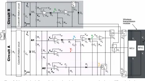
Figure 2 shows a proposed circuit without bypass ca- pacitors, current-limiting resistors, damping resistors, and voltage reference generators. The resistors R0and R11 are load resistors for the CT. The circuit A including R0 and B including R11 are for measuring low and high cur- rent flow, respectively. The devices U0-4,10,11 are com- parators and U5-9,12 are analog switches. The Cock- croft-Walton (CW) circuits [6] are used as stepup con- verter in both circuit A and B. The power sources of the devices U0-9 and the others U10-12 are charged capacitor
C0 and C4, respectively. The all voltage references Vref
are same value and generated by bandgap reference gen- erators in both circuits. The circuit A has the circuit A1 and A2 to change the power source for the wireless transmission module depending on current flowing through a power line. The circuit A1 switches the charg- ing circuit from the circuit A to B if the measuring cur- rent exceeds a threshold value. The circuit A2 turns the charging circuit back.
Figure 3 shows the relationship between measuring current I0 and the charging circuits. IA and IB represent I0 when power charged by the circuit A and B is used for wireless transmission, respectively. Ith_up and Ith_down are
[image:2.595.59.285.581.696.2]threshold current for switching the charging circuit from the circuit A to B and from the circuit B to A, respec- tively. These threshold values are set different values to make behaviors of this circuit stable.
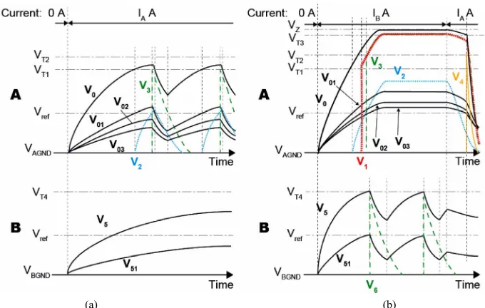
Figure 4 shows the voltage changes at the points V0-6 of the circuit in Figure 2. Figures 4(a) and (b) indicate the case of low and high current I0, respectively. VT1, VT2,
VT3, and VT4 represent the threshold voltages for V0 at U0,
U1, U2, and U10, respectively. VZ shows the zener volt-
age of DZ0 and DZ1.
First, behaviors of the circuit in the case of Figure 4(a) are explained below. When current IA flows through a
measured power line, voltage V0 exceeds VT1, but V5 does not increase up to VT1. When V0 increases up to VT1, the output of comparator U0 changes from low to high level. The resistor R7 and the capacitor C2 compose a delay cir- cuit. The voltage V2 increases up to the voltage produced by a voltage divider (R7 and R9) according to the time constant (R7 × C2). When V2 increases up to Vref, the out-
Figure 2. Schematic circuit diagram for battery-less wireless current sensor node using two different load resister.
In Figure 4(b), V0 exceeds VT2 during the above men- tioned delay, then the output of comparator U1 becomes high level. The analog switches U8 and U9 change the power source from C0 to C4 and the output of analog switch U7 changes the connection of a micro controller unit (MCU) from VAGND to the analog switch U12. At this time, since the power charged in C0 is not used for the wireless transmission, V0 increases up to the voltage which depends on the power consumption of circuit A and the power obtained from the CT. In this case, al- though V0 can exceed withstand voltages of the devices used in the circuit A, the zener diode DZ0 is used to pre- vent breakdowns of the devices. In the circuit B, wireless transmission is performed like the circuit A every time when the voltage V5 increases up to VT4. At the connec- tion between U12 and the circuit A, influence of pulsating voltage must be prevented. Although V5 is DC voltage if
VBGND is the reference voltage, V5 is pulsating voltage if
VAGND is the reference voltage. Since behavior of U12 can be unstable by the pulsating voltage, the effect is de- creased using the diode D5.
Figure 3. Relationship between measuring current I0 and charging circuits.
rate of V0 exceeds a threshold voltage can be detected. In other words, if V0 increases up to V2 during the delay, this circuit can detect that I0 exceeds Ith_up. In the case of
Figure 4(a), I0 is less than Ith_up. When the output of the
comparator U3 becomes high level, the output of the comparatorU4 also changes to high level immediately. The analog switch U6 connects C0 to the wireless trans- mission module, then the module starts wireless trans- mission. At this time, V0 drops without delay, then out- put of U0 becomes low level. However, the output of U4 keeps high level by the delay circuits composed of C2, R9,
C3, and R10 until the wireless transmission finishes. U8 and U9 are analog switches for switching the power sources charged by the circuit A or B. The output of analog switch U7 indicates which power source is used. Low and high level of output of U7 shows that the wire- less transmission is performed using the power charged by the circuit A and B, respectively. The transmitted packet includes an identification number of the wireless sensor node and one bit data that indicates which power source is used, but does not includes current data.
When I0 decreases from IB to Ith_down, V0 does not de- crease to VT2. Because the power consumption of the circuit A except for wireless transmission is small. Actu- ally, V0 does not decrease to VT2 unless I0 decreases to around minimum of the measurable range. The current
IA0 in Figure 3 indicates I0 at which V0 decreases to VT2. In this case, the power charged by the circuit B cannot be charged enough for the wireless transmission if I0 is lower than Ith_down. Thus, the power charged by the circuit
[image:3.595.68.275.365.445.2](a) (b)
Figure 4. Voltage changes at the points V0-6 of the circuit in Figure 2. (a) and (b) indicate the case of low a high current I0, respectively.
0
reased to less than VT2. The circuit A2 can detect an
d wireless current sensor om 0.5 A to 50 A in which
The resistance values of R1-6,12,13 which al
reduce the power consumption. CTL-10-CLS (UR_D),
VICES) and LTC1540 (LINER TECHNOLOGY) were
U1 to high level at the Ith_up. In this case, VT2 was 2.29 V. nd
Ith_down. To change the power source, V need to be de- MCP644x (MICROCHIP), ADG849 (ANALOG DE-
c
event at which I0 decreases to Ith_down and decrease V0. The output of the comparator U2 becomes high level when V0 decreases to the voltage VT3 at which I0 is Ith_down.
This high level signal must be changed to low level im- mediately after V0 decrease to VT2. Because U5 continues to connect V0 and VAGNDif the output of U2 is high level. In this case, power cannot be charged in C0. To make one shot pulse signal, this high level signal is differentiated by a differentiator composed of the capacitor C1 and the resistor R8. The analog switch U5 connects VAGND with V0 through a current limiting resistor only for the time of the pulse width, then V0 drops to less than VT2. The diode D3 is intended for preventing a signal which is generated when the output of U2 changes from high to low level. If
D3 is not in this circuit, the circuit B cannot be used to charge the power for wireless transmission. Because the power is consumed every time when V0 exceeds VT3.
3. Experimental Result
In this research, we designe node with measurable range fr
the transmission intervals are less than 0.5 s. The 3 stage CW circuit was used in the circuit A and B. We have not examined how many stages of the CW and how much capacitors used in the CW circuit are suitable for this current sensor.
Table 1 shows the designed values of the resistors and the capacitors.
ways consume the current were more than 10 MΩ to
used as a CT, comparators, analog switches, voltage ref- erence generators, respectively. A wireless sensor mod- ule was mainly composed of C8051F930 (Silicon labs) used as MCU and nRF24L01 (Nordic) used as RF IC. The voltage reference was 1.182 V [7]. The conditions [5] of the wireless transmission were same with except for the packet structure. Since the lower limit voltage at which both two ICs work was 1.8 V [8,9], VT1 must be more than 1.8 V. In this research, we determined VT1 was 2.15 V. In this case, since the required charge for the wireless transmission was about 4.18 μAs [5], the ca- pacitance values of C0 and C4 must be more than 11.9 μF. On the other hand, these capacitors have a function to smooth ripples. In this research, we determined the ca- pacitance values of C0 and C4were 0.8 mF and 1.3 mF, respectively. The reason that the capacitance of C4 is larger than C0 is that IB is higher than IA. The resistance
values of R10,14 and the capacitance values C3,5 were de- termined according to [5]. The output voltage of the CW circuit depends on the load. First, the resistance values of
R1-6 were temporarily set to 10 MΩ in order to fix the load. Next, resistance value of R0 by which V0 exceeds the VT1 when I0 is 0.5 A was determined. Not to become the transmission interval (ttrans) short, small resistance is better. In this research, we determined the resistance value of R0 was 6.2 kΩ. In this case, the transmission intervals were almost not changed if I0 exceeded about 6 A. Thus, we determined Ith_up and Ith_down were 6.5 A and
Table 1. Values of the resistors and capacitors in Figure 2.
Resistor Resistance (Ω) Capacitor Capacitance (F)
R0 6.2 k C0 1.3 m
R1 10 M C1 1 μ
R2 12.2 M C2 0.2 μ
R 10 M C 0.02 μ
4 4
5 20. 5
3
R
3
C
10.68 M 0.8 m
R 51 M C 0.02 μ
R6 10 M
R7 910 k
R8 110 k
R9 2.2 M
R10 820 k
R 11
R12
220
10 M
R13 11 M
R14 820 k
The voltage V5 s to exceed V at Ith_down. In the cir-
cuit B, the wi issions were someti
perf r ed if VT oVT1. The reason has not clari- fied but we th ripp s gen ated by the step up converter can the stability. Thus, we determined
T4 was 2.26 V. If the resistance values of R12,13 were set
d clamped the double or triple power lines. The fre
easure current fr
need T4
reless transm mes not
o m 4 equaled t
ought le er
affect
V
to 10 MΩ and 11 MΩ, respectively, it was found that V5 exceeded VT4 at 220 Ω of the resistance R11. The resis- tance values of R5,6 were set to change the output of U2 from low to high level at Ith_down. In this case, VT3 was 3.61 V.
Figure 5 shows the experimental setup. In this meas- urement, current calibrating apparatus (FLUKE 5080 A), the maximum current of which is 20.5 A, was used. When we measured transmission interval at more than 20.5 A, the power line was wrapped one time or two times an
quency of AC current was 50 Hz. The transmission interval was measured by a receiver system that can save times when the receiver receives packets.
Figure 6 shows the results. The solid and dotted line indicates that the transmissions were performed using the power charged by the circuit A and circuit B, respec- tively. The each point is the average of ten measured intervals and the error bars are also shown. This graph shows this wireless sensor node can m
om 0.5 A to 50 A. Table 2 shows the differences be-tween this work and [5].
4. Conclusion
In this research, the battery-less wireless current sensor
Figure 5. Experimental setup.
[image:5.595.55.287.102.352.2]Figure 6. Relationship between current flowing through a power line and transmission interval.
Table 2. Differences between this work and [5].
This work [5]
Number of CTs 1 1
Number of charging circuits 2 1
Example of measurable range (Double digits) 0.5 A - 50 A (Single d2 A - 20igit) A
n ging time depend on r-
rent flowing through a power line was developed. In this
ty problem that the measurable
range is about single digit si rgi e-
c re re is
aper, we proposed the circuit in which two load resis-
cce, 26-29 October 2008, pp. 625- 628.
ode using that the char is the cu
pe of sensor, there is a
nce the cha d current inc
ng time b ases. In th omes short as the measu
p
tors were used, and demonstrates that the node can meas- ure current flowing thorough a power line from 0.5 A to 50 A. If the step-up converter and the resistors of R1-6,12,13 are optimized or lower power consumed devices than the devices used in this research are utilized, the measurable range can be expanded.
REFERENCES
[image:5.595.309.537.409.492.2][2] S. G. Taylor, K. M. Farinholt, E. B. Flynn, E. Figueiredo, D. L. Mascarenas, E. A. Moro, G. Park, M. D. Todd and C. R. Farrar, “A Mobile-Agent-Based Wireless Sensing Network for Structural Monitoring Applications,” Meas- urement Science & Technology, Vol. 20, No. 4, 2009, pp. 1-14. http://dx.doi.org/10.1088/0957-0233/20/4/045201 J. Hay
[3] es, S. Beirne, K.-T. Lau and D. Diamond, “Evalua- tion of a Low Cost Wireless Chemical Sensor Network for Environmental Monitoring,” Proceedings of IEEE Sensors, Lecce, 26-29 October 2008, pp. 530-538. [4] T. Itoh, Y. Zhang, M. Matsumoto and T. Maeda, “Wire-
less Sensor Network for Power Consumption Reduction in Information and Communication Systems,” Proceed- ings of IEEE Sensors, Christchurch, 25-28 October 2009, pp. 572-575.
[5] H. Okada and T. Itoh, “Battery-Less Wireless Current Sensor Node Utilizing the Dependence of Charging Time of a Capacitor on the Current Flowing through a Power Line,” IEICE Electronics Express, Vol. 10, No. 12, 2013. http://dx.doi.org/10.1587/elex.10.20130308
[6] J. D. Cockcroft and E. T. S. Walton, “Experiments with High Velocity Positive Ions. (I) Further Developments in the Method of Obtaining High Velocity Positive Ions,” Proceedings of the Royal Society A, Vol. 136, 1932, pp. 619-630. http://dx.doi.org/10.1098/rspa.1932.0107 [7] Linear technology: datasheet of LTC1540, p. 5.
[8] Silicon laboratories: datasheets of C8051F93x-C8051F92x, p. 46.