Parallel Self Timed Adder using Gate Diffusion
Input Logic
Elina K Shaji Abraham K Thomas
PG Student Assistant Professor
Department of Electronics & Communication Engineering Department of Electronics & Communication Engineering Saintgits College of Engineering Saintgits College of Engineering
Susan Abe
Professor
Department of Electronics & Communication Engineering Saintgits College of Engineering
Abstract
In modern technology, power dissipation has become a major and vital constraint in electronic industry. Gate diffusion Input (GDI) is a technique that lowers power dissipation to a greater extend. This technique also reduces the transistor count, area and thus the complexity of the circuit. The circuit will be much simpler and easy to manage. This paper describes the design of a 16 bit Parallel Self Timed Adder (PASTA) using GDI logic. PASTA is an asynchronous adder and is based on a recursive formulation for performing multi-bit binary addition. The operation of PASTA is parallel for those bits that do not require any carry chain propagation. PASTA design uses multiplexers along with half adders. All the carriers are detected using a completion signal detection unit which will enable the selection line of multiplexer which produces high fan out. One of the limitations is high fan in, but this is unavoidable for asynchronous logic. The simulation results show the proposed model attains better power consumption and reduction in number of transistors.
Keywords: Asynchronous Circuits, Binary Adders, CMOS Design
________________________________________________________________________________________________________
I.
INTRODUCTION
An adder or a summer is a digital circuit that performs addition of numbers. Addition forms the basis for many processing operations, from counting, multiplications to filtering. In processors adders are also used to increment program counters, calculate effective addresses, table indices and similar operations. Thus the performance of processor is greatly influenced by the speed of the adders used by the processor.
Circuits may be classified as synchronous or asynchronous. Synchronous circuits are based on clock pulse. That is synchronous systems comprise a number of subsystems that uses a clock to synchronize their operations. Asynchronous circuits is one in which there is no global synchronization within the system. The results produced by the subsystems in an asynchronous system can be consumed by other subsystems as soon as they are generated without having to wait for a global clock pulse. Subsystems within the system are synchronized locally by the communication protocols between them. An asynchronous system involves request/acknowledge handshake signaling protocol. The synchronous adders perform slowly due to its incremental nature of operation and therefore it is not recommended for fast and parallel adders.
The basic building block of combinational digital adders is a single bit adder. The simplest single bit adder is a half adder (HA). The full adders (FA) are single bit adders with the carry input and output. The full adders are basically made of two half adders in terms of area, interconnection and time complexity.
Addition is a special prefix problem that each sum bit is dependent on all equal or lower input bits. Implementing a parallel algorithm for addition thus becomes difficult due to this dependency. But the flow of bits can tactfully arrange that can reduce the addition overhead significantly by using a tree structured implementation of the adder. Carry Look Ahead adders, Carry Save adders, Carry Skip Adders are examples of this type of adders.
for storing the states of the subsystems. In a synchronous circuit the current state of the circuit is stored in an array of registers. The next state is computed from the current state and inputs by a combinational logic circuit. When the clock signal makes a transition either a low to high or a high to low, the registers are enabled, and the next state is copied into the registers, thus becoming the current state. Each register bit generally comprises two latches, usually cascaded into a master slave flip-flop. A clock based system (synchronous system) can operate correctly only if all parts of the system get the clock at the same time. It can happen only if the delay is negligible on the clock wire. Present day, the systems tend to get bigger and bigger in terms of the number of transistors. As a result the delay on the clock wires cannot be ignored. The problem of clock skew is thus a major limitation for many system designers. A solution to this problem is to distribute the global clock using a clock network with clock buffers, thereby controlling the clock skew. But, this results in rise in the capacitance of the clock network and may suffer from increase activity.
Another problem is the power dissipation which becomes more important due to the phenomenal growth of portable devices. Average power consumption has become the most critical design concern for mobile electronics applications. Clock based systems tend to consume more power than necessary. Many gates switch unnecessarily since they are connected to the clock and not because they have to process new input data.
Asynchronous Circuit: B.
Asynchronous systems are not based on clock. Such a system tends to have better noise and electromagnetic compatibility properties than synchronous systems due to the absence of a global clock reference. Asynchronous operation by itself does not imply low power, but often suggests low power opportunities based on the observation that asynchronous circuits consume power only when it is active.
An asynchronous system is a system in which there is no global synchronization within the subsystems. Asynchronous circuits do not assume any quantization of time (“C H. Van Berkel et.al., September 1998”). They hold great potential for logic design as they are free from several problems of clocked or synchronous circuits. Systems are synchronized locally by the communication protocol between them. Usually a request acknowledgment handshaking protocol is used to establish a communication between the subsystem in the absence of clocks. In asynchronous systems, a subsystem can be replaced by another subsystem with the same functionality but with different performance. But this is not an easy task for a synchronous circuit as the clock period might have to be recomputed.
PASTA: C.
Fig. 1: Block Diagram of PASTA (“Mohammed Ziaur et.al.,2015”)
Architecture of PASTA: D.
The architecture of PASTA is shown in figure 2.1. The two input multiplexer has selection input that corresponds to the request handshake signal and will be a single zero to one transition denoted by SEL. It will first select the actual operand during SEL = 0 and will switch to feedback paths for subsequent iterations using SEL = 1. The feedback path from the HAs enables the multiple iterations to continue until the completion when all carry signals will assume zero values.
A CMOS implementation for the multiplexer, Half Adder and the completion detection unit is shown in fig. 2.2, 2.3, 2.4, 2.5
Fig. 4: Circuit Diagram Of HA Sum & Carry Module (“Mohammed Ziaur Et.Al.,2015”)
Fig. 5: Circuit Diagram of Completion Detection Unit (“Mohammed Ziaur et.al.,2015”)
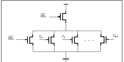
The completion detection circuit is used to obtain an active high completion signal (TERM). This requires a large fan in n input NOR gate. Therefore, a more practical pseudo nMOS ratioed design is used. Using the pseudo nMOS design, the completion unit avoids the high fan in problems as all the connections are parallel. The pMOS transistor connected to VDD of this ratioed design acts as a load register, resulting in static current drain when some of the nMOS transistors are on simultaneously (“Mohammed Ziaur et.al., 2015”). The negative of SEL is also included for the TERM signal to ensure that the completion cannot be accidentally turned on when the actual inputs are initially selected. Design also restricts the pull up transistor pMOS being from always turned on. Therefore, static current will be flowing only for the duration of the actual computation.
III.
ANALYTICAL PROCEDURES
Transistor count is the primary concern which affects the design complexity of the circuit. For submicron CMOS technology area, topology selection, power dissipation and speed are very important for high speed and low power applications. But the proposed PASTA design has the drawback of high power consumption and uses large number of transistors which further increases area. This issue can be overcome by Gated Diffusion Input (GDI) technique (“Arkaidy Morgenshtein et.al., 2002”).
GDI Cell: A.
Fig. 6: GDI Basic Cell (“Arkadiy Morgenshtein Et.Al.,2002”)
It resembles CMOS inverter in the first glance. The important difference of GDI cell from CMOS inverter is that it has three inputs. The GDI cell contains four terminals: three input node and an output node. The three inputs are: G: The common gate input of nMOS and pMOS, P: Input to the source of drain of pMOS, N: Input to the source or drain of nMOS. The output node: The common diffusion node of both transistors. It can be used as input or output nodes.
Using this technique several large functions can be implemented using less number of transistor counts. The GDI approach uses two transistors for implementing various complex logic functions. This method is suitable for design of fast, low power circuits using a reduced number of transistors when compared to CMOS, while improving logic level swing and static power characteristics. Multiple input gates can be implemented by combining several GDI cells.
PASTA using GDI Logic: B.
The proposed PASTA using GDI logic is shown in Fig 3.2. The design consists of multiplexer, Half Adders and completion detection unit. The two input multiplexers has selection inputs that corresponds to request handshake signal and will be a single 0 to 1 transition denoted by SEL. It will initially select the actual operands during SEL = 0 and will switch to feedback paths using SEL = 1for subsequent iterations. The feedback path from Half Adders enables the multiple iterations to continue until the completion when all carry signals will assume zero values.
Fig. 7: Block Diagram Of PASTA (“Mohammed Ziaur Et.Al.,2015)
The Half Adder is the building block of all arithmetic circuits. Every microchip or machine that can perform addition, subtraction, multiplication, or division has Half Adders blocks inside. So it is the first area to work on building a low power design. By implementing the Half Adder using GDI logic the transistor count can be reduced there by reduction in power consumption can be observed. Traditional CMOS Half Adders has two separate circuits for sum and carry module. But for Half Adders implemented using GDI logic, both sum and carry module are merged into the single circuit as to perform half adder operation. Design of a HA using GDI logic is shown in figure 3.3.
Fig. 9: Half Adder With GDI Logic (“Silpa T S Et.Al., 2015”)
Design of Multiplexer: D.
Multiplexer using GDI logic reduces the transistor count of which is found to be more power efficient in comparison with existing multiplexer design that ultimately reduces the power dissipation and area of digital circuits while maintaining low complexity of logic design. Design of a multiplexer using GDI logic is shown in figure 3.4.
IV.
RESULTS AND DISCUSSION
In order to understand the effectiveness of the proposed design, the performance of the proposed PASTA is evaluated against existing PASTA with CMOS design. The Pyxis schematic of Mentor Graphics is used in order to create the schematics of the circuit. The performance of the PASTA using GDI design is evaluated against existing designs through pre-layout simulations using eldo simulator. The output waveforms are viewed using E-Z wave viewer. The target technology is the TSMC 180-nm CMOS process. The operating condition used in simulations is 500 MHz/5V. In order to analyze the power consumption data pattern with 100% transition probability is given at a temperature of 27oC.
Graphs for PASTA with CMOS Design: A.
The delay of the PASTA with CMOS design is shown in figure 4.1.
Fig. 11: Delay Waveforms Of The PASTA With CMOS Design
Graph for Proposed PASTA: B.
influenced by the speed of the adders used. The design of Parallel Self Timed Adder (PASTA) is regular and uses half adders along with multiplexers with minimum interconnection requirement. The architectural design and CMOS implementation are presented. But the design has the drawback of high power consumption and uses large number of transistors which increases area when compared with synchronous adders. This issue is overcome by implementing the PASTA with Gate Diffusion Input (GDI) technique. The design achieves a very simple n bit adder that is area, interconnection and power consumption wise more efficient than the previous self timed adder. Also, the circuit works in a parallel manner for independent carry chains, and thus achieves logarithmic average time performance over random input values.
REFERENCES
[1] Arkaidy Morghenshtein, Alexander Fish and Israel A. Wagner, “Gate diffusion input (GDI) – A technique for low power design of digital circuits; Analysis
and characterization”.
[2] Arun Prakash Singh, Rohit Kumar, “Implementation of 1- bit full adder using gate diffusion input (GDI) cell” International Journal of Electronics and Computer Science Engineering.
[3] S Bharathi, M. Sunandha Preethi, “Area Efficient Self Timed Adders for Low Power Applications in VLSI”, International Journal of innovative Research
in Science, Engineering and Technology, Vol. 4, Issue 2, February 2015.
[4] J. Dhanasekar, S. Sarmila, V. Kavitha, S. Rathimeena, “Power Analysis of Parallel Self Timed Adder by Recursive Method”, International Journal of Advanced Engineering Research and Technology (IJAERT), Vol. 2 issue 6, September 2014.
[5] Fu-Chiung Cheng, Stephen H. Unger, Michael Theobald “Self-Timed Carry-Lookahead Adders”, IEEE Transactions on Computers, vol. 49, no.7, July
2000
[6] D. Geer, “Is it Time for Clockless Chips, [Asynchronous Processor Chips],” Ieee Transactions on Computers, Vol. 38, no. 3, pp. 18-19, March 2005.
[7] Jein Chung Lo, “A Fast Binary adder with Condutional Carry Generation”, Ieee Transactions on Computers, Vol. 46, No. 2, February 1997.
[8] Mohab Anis, Mohamed Allam, Mohammed Elmasry, “Impact of Technology Scaling on CMOS Logic Styles”, Ieee Transactions on Circuits and Systems
2: Analog and Digital Signal Processing, Vol. 49, No. 8, August 2002.
[9] Mohammed Ziaur Rahman, Lindsay Kleeman, and Mohammad Ashfak Habib, “Recursive Approach to the Design of a Parallel Self-Timed Adder,” IEEE
Transaction on Very Large Scale Integration (VLSI) Systems, vol. 23, no. 1, January 2015.
[10] A Morgenshtein, A Fish and I A. Wagner “Gate-Diffusion Input (GDI) – A Power Efficient method for Digital Circuits: A detailed Methodology,” in 14th
Ieee Int. ASIC/SOC Conf., September 2001.
[11] S. Nowick, “Design of a Low Latency Asynchronous Adder using Speculative Completion”, Ieee Proc. Comput. Digital Tech., vol. 143, no. 5, September
1996.
[12] Silpa T S, Athira V R “Power Efficient Arithmetic Logic Unit”, International Journal of Engineering and Technical Research (IJETR), ISSN: 2321-0869,
Vol. 3, Issue 2, February 2015.
[13] J. Sparso and S. Furber, “Principles of Asynchronous Circuit Design”, Boston, MA, USA: Kluwer Academic, 2001.
[14] M. Z. Rahman and L. Kleeman, “A Delay matched approach for the Design of Asynchronous Sequential Circuits,” Dept. Computer Syst. Technol., Univ.
Malaya, Kuala Lumpur, Malaysia, Tech. Rep.05042013, 2013