ProQuest Number: 13832055
All rights reserved INFORMATION TO ALL USERS
The qu ality of this repro d u ctio n is d e p e n d e n t upon the q u ality of the copy subm itted. In the unlikely e v e n t that the a u th o r did not send a c o m p le te m anuscript and there are missing pages, these will be note d . Also, if m aterial had to be rem oved,
a n o te will in d ica te the deletion.
uest
ProQuest 13832055
Published by ProQuest LLC(2019). C op yrig ht of the Dissertation is held by the Author. All rights reserved.
This work is protected against unauthorized copying under Title 17, United States C o d e M icroform Edition © ProQuest LLC.
ProQuest LLC.
789 East Eisenhower Parkway P.O. Box 1346
ACKNOWLEDGEMENTS.
I would first of all like to say a big thank you to my supervisor Stewart Aitchison for his invaluable guidance, support, encouragement, patience and friendship.
I would also like to express my appreciation to all the technical staff in the Engineering department for their help and advice, especially those staff that I pestered on a weekly basis including: Dave Clifton, Gillian, Jim Gray, Jimmy Young, Joan Carson and last but not least Robert Harkins.
I am also greatly indebted to the following people without whose help there wouldn't have been much of a thesis to write: Gordon Kennedy and W ilson Sibbett from St Andrews University, Jin Kang and George Stegeman from the University of Central Florida and Alain Villeneuve from the Universite Laval.
I am also very grateful to all the research staff and students at Glasgow University that I've came to know over the past few years and would like to thank them all for their friendship and help and for the fond hazy memories I have of nights out at the "Doublet". In particular, I would like to thank my old pal Jude for being a great friend and for accompanying me to the "Beer Bar" in times of despair and boredom. Finally I would like to say a huge big thank you to my family and my boyfriend Richie for their love and support and for helping me through many a PhD panic attack,
ABSTRACT.
The main objectives of this research project related to the observation of ultrafast, all-optical switching within AlGaAs structures operated in the half-band gap spectral region. The switching configurations investigated were based on nonlinear periodic structures and included nonlinear waveguide arrays and Bragg gratings.
PUBLICATIONS.
Conference Publications.
P.M illar, C.J.Ham ilton, J.S.A itchison, G .T.K ennedy and W .Sibbett, "Nonlinear three core couplers in AlGaAs", QE-12 Technical Digest, p l- 22 (1995).
P .M illar, J.S .A itch iso n , J.U .K ang, G .I.S teg em an , A .V illeneuve, "N onlinear m ulti-core directional couplers in A lG aA s", N onlinear Guided W aves and their Applications, Opt.Soc.Am. Technical Digest Series, 15, pp 125-127 (1996).
Journal Publications.
P .M illar, R .H arkins and J.S.A itchison, "F abrication of low loss, w av e g u id e g ratin g filte rs u sin g e lec tro n b ea m lith o g ra p h y " Electron. Lett., 33, pp 1031-1032 (1997).
CONTENTS.
A c k n o w le d g e m e n t s ... I A b s tr a c t ... Ill P u b lic a tio n s ...IV C o n te n ts...V-VIIII
Chapter One: Introduction.
In tr o d u c t io n ...1
1 .1 .1 . The evolution of communications system s...2
1 .1 .2 . A ll-optical sw itching... 3
1 .2 . O bjectives of research... 3
1 .3 . N onlinear O ptics...4
1 .4 . N onlinear E ffects... 4
1 .4 .1 . Second order nonlinearities...5-6 1 .4 .2 . Third order nonlinearities... 7-13 1 .4 .2 .1 . The optical Kerr effect... 7-8 1 .4 .2 .2 . Self phase m odulation...9-10 1 .4 .2 .3 . S elf-focusing... 11
1 .4 .2 .4 . S olitons... 11-13 1 .4 .2 .4 .1 . Spatial solitons...11-12 1 .4 .2 .4 .2 . Tem poral solitons... 12
1 .4 .2 .4 .3 . Bragg Solitons... 13
1 .4 .2 .4 .4 . Gap solitons... 13
Chapter Two: The Nonlinear Optical Properties of
AlGaAs.
I n tr o d u c t io n ... 17 2 . 1 . 1 . The crystal structure of A lGaAs...18
2 . 1 . 2 . Fabrication of A lG aA s... 19-20
2 . 2 . Band structure of III-V ... 20-21 compound semiconductors.
2 . 3 . Types of nonlinearities in direct band... 21-22 gap semiconductors.
2 . 3 . 1 . R esonant nonlinearities...22
2 . 3 . 2 . N onresonant nonlinearities...22
2 . 4 . M easurement of the nonlinear coefficient... 23-25
2 . 4 . 1 . K ram ers-K ronig relatio n... 23
2 . 4 . 2 . Higher band m odels... 24-25
2 . 5 . Multi-photon absorption in AlGaAs waveguides...25-30
2 . 5 . 1 . Two photon absorption... 26-28
2 . 5 . 2 . Three-photon absorption...29-31 2 .6 . C onclusions...31
Chapter Three: Semiconductor Waveguide Design,
Fabrication and Charactersiation.
I n t r o d u c t io n...33
3 . 1 . Properties of semiconductor optical waveguides...34-35
3 . 2 . Basic optical waveguide theory...35-41
3 . 2 . 1 . Snell's law and total internal reflection...35-36
3 . 2 . 2 . Propagation of light in a dielectric slab... 37-38
3 . 3 . 3 . M axwell's equations...38-41 3 .3 . Optical waveguide design... 41-46 3 .3 .1 . W aveguide geom etry...42
3 . 3 . 2 . Sources of linear loss w ithin... 43-44 semiconductor waveguides.
3 .3 .3 . W afer com position... 44
3 . 3 . 4 . Estimation of the propagation constant...44-46
3 .3 .4 .2 . The scalar finite difference m ethod... 46 3 .4 . Fabrication of the optical waveguides...47-49 3 .4 .1 . Photolithography...47-48 3 .4 .2 . Reactive ion etching...49 3 .5 . W aveguide loss m easurem ent... 49-52 3 .6 . Nonlinear properties of AlGaAs w aveguides... 52-61 3 .6 .1 . Experimental arrangement used to test...52-55
the nonlinear devices.
3 .6 .1 .1 . M odelocking... 53 3 .6 .1 .2 . Active mode locking by synchronous pum ping...54 3 .6 .1 .3 . Passive mode locking using a coupled... 55
cavity mode locking technique.
3 .6 .2 . Measurement of the nonlinear refractive index... 55-58 coefficient.
3 .6 .3 . Measurement of the two photon absorption... 58-61 coefficient.
3 .7 . C onclusions...62
Chapter Four: Nonlinear Coupled Waveguide
Arrays.
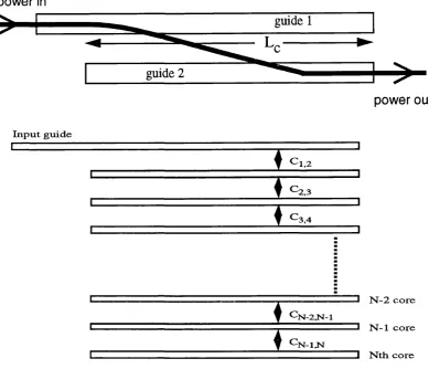
I n tr o d u c tio n...65 4 .1 . The linear directional coupler... 66-70 4 .2 . Development of the nonlinear coupler array... 70-71 4 .3 . Nonlinear coupler theory...72-74 4 .4 . Applications of nonlinear coupler devices...74-75 4 .4 .1 . Nonlinear waveguide arrays and soliton sw itching... 76 4 .5 . Theoretical modelling of nonlinear coupler arrays 77-98 4 .5 .1 . Temporal beam propagation m ethod... 77-80 4 .5 .2 . Spatial beam propagation m ethod... 81 4 .5 .3 . Theoretical simulations of the switching... 81-89
characteristics of nonlinear coupled arrays.
4 .5 .3 .1 . Simulations of the switching behaviour o f... 83 a nonlinear three core coupler.
4 .6 . Design and fabrication of the nonlinear arrays... 90 4 .7 . Experimental investigation of the...91-92
nonlinear coupled arrays.
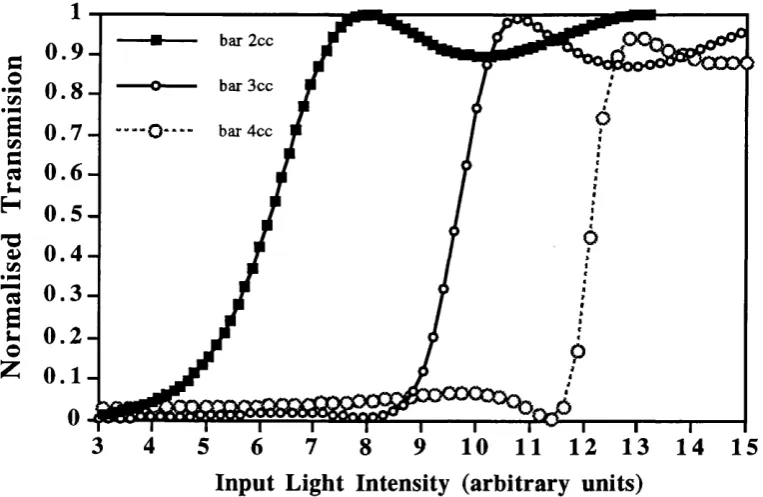
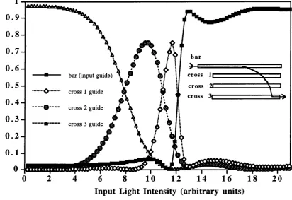
4 .8 . Experim ental results...93-105 4 .8 .1 . Three guide nonlinear coupler experim ents... 93-102 4 .8 .1 .1 . The centre launched three guide coupler...93-95 4 .8 .1 .2 . The side launched, uniformly spaced...96-99
three guide coupler.
4 .8 .1 .3 . The side launched,non-uniformly spaced... 99-101 three guide coupler.
4 .8 .2 . M ulti-guide nonlinear coupler experim ents... 102-105 4 .8 .2 .1 . The four guide nonlinear coupler experim ent...102-103 4 .8 .2 .2 . The eight guide nonlinear coupler experim ent... 104-105 4 .9 . C onclusions...106
Chapter Five: Grating Structures.
I n tr o d u c tio n ... 114
5 .1 . Grating structures and their applications...115-116 5 .2 . Grating theory... 116-120 5 .2 .1 . Linear grating theory... 116-119 5 .2 .2 . N onlinear grating theory... 119-120 5 .3 . Theoretical modelling of the nonlinear D FB...120-123 5 .4 . Design of the grating switch... 124-125 5 .5 . Device fabrication... 125-130 5 .5 .1 . Fabrication of the waveguide filter using an...125-130
holographic process.
5 .5 .2 . E-beam lithography... 130-133 5.6. Experim ental results...135-146 5 .6 .1 . Linear characterisation of th e... 134-135
holographic gratings.
5 .6 .2 . Linear loss measurements of the holographic gratings 135 5 .6 .3 . Linear characterisation o f... 136
the e-beam written gratings.
5 .7 . Chirped gratings... 143-146 5 .8 . Suggested further w ork... 147 5 .9 C onclusions... 148
Chapter Six: Summary of Thesis.
6 . 1 . Conclusions on the design and... 151 modelling of the nonlinear devices.
6 .2 . Conclusions on the fabrication of the nonlinear devices 152
6 .3 . Conclusions on the experimental results...152-153 6 .3 .1 . Experimental results on the waveguide arrays... 152
and suggested future work.
6 .3 . 2 . Experimental results on the grating structures ... 153 and suggested future work.
CHAPTER 1
Introduction.
1.1. Introduction.
In this thesis the switching characteristics of several different all-optical switching devices were investigated. This introductory chapter will outline the aims and objectives of the thesis and will present an introduction to nonlinear optics and all-optical switching.
The Evolution of Communications Systems.
Telecommunication systems have come a long way since the production of the first optical fibres in the mid-sixties. The increasing demands made by the market place, in combination with new technological advances, have produced a communications revolution. The internet (including electronic mail), video-phones, faxes, long-haul fibre telecommunication networks, satellite systems for TV and scientific applications are some of the recent advances in communications. These new applications have been brought about by improved low loss optical fibres networks, efficient laser diodes, optical fibre amplifiers, advances in integrated circuit technology ( VLSI and ULSI) and the use of nonlinear optical devices. However, the communication revolution is by no means over and further research is needed to refine, exploit and improve the technology and systems in use today.
In the future, demands placed on optical communication and computing systems will increase so much so that new improved networks will be needed. Vital to the development of these new networks is the production of ultrafast switching components for information processing.
1 . 1 . 2 . All-O ptical Switching.
To m ake better use of the information capacity of optical networks, by expanding the usable bandwidth of these systems, it is envisaged that, in the future, inform ation processing will be conducted using all-optical switches/logic gates based on nonlinear optical effects. All-optical switches h ave great potential for fu tu re com m unications and com puting applications for several reasons. One major advantage over electronic gates is that the speed of an all-optical switch depends solely on the speed of the nonlinearity which for a nonresonant nonlinearity can be effectively instantaneous. In addition, all-optical switches are not affected by magnetic, or electric disturbances as is the case for electrical components. Furtherm ore, processing all-optically has the added advantage that bottlenecks caused by the conversion between optics and electronics are elim inated. Therefore, by processing all-optically not only would both time and energy be saved but the information carrying capacity of optical fibre networks would increase.
1 .2 . Objectives of Research.
1 .3 . Nonlinear Optics.
Nonlinear optics is the term used to described the changes in the optical properties of a material caused by the interaction of intense light with the m aterial. To observe nonlinear effects a high intensity optical field, i.e .- 2.5 kW /cm 2 is required. Therefore research into nonlinear optic behaviour did not begin until the demonstration of the first operational, pulsed ruby, laser by Mainman in 1960. Before that the available light sources were not intense enough to produce nonlinear effects. The first nonlinear effect to be observed was the discovery of second harmonic generation by Franken et al2. Since then, a wide variety of optically nonlinear phenomenon have been explored in many different material system s including sem iconductors, glasses and in nonlinear organic m aterials in various m acroscopic forms i.e., crystals, liquid crystals, polym ers and films. In the following section some of these nonlinear effects are described.
1 .4 . N onlinear Effects.
The nonlinear response of m atter to an incident light field may be w ritten3:
P, = e.
' " l X„(I>E; + X x / ’E jE , + S X iW ^ E jE jE ,+..
V
j
ik
J
(1.1)Second O rd e r N o n lin e aritie s.
A ssu m in g the third and subsequent higher order susceptibilities are zero,
equation 1.1 can be written as:
Pi =£o[l%ij{1)Ej + lXijk{2)EjEk]
(1
.2
)j j k
W h e re y (2) is the second order nonlinear susceptibility w hich gives rise to
nonlinear effects such as second harm onic generation, sum and difference
f re q u e n c y m ix in g and op tical p a ra m e tric o sc illa tio n . S e c o n d o rd er
n o nlinear effects can only occur in crystals that are noncentrosym m etric,
i.e. do not display inversion symmetry, such as G aA s and Lithium niobate.
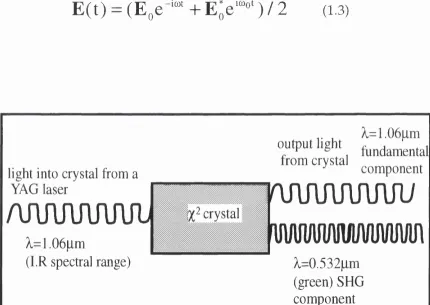
Figure 1.1 is a schem atic o f the second harm o n ic effect. The radiation
from the Y A G laser produces intense laser light at 1.06 pm . Supposing the
time dependent part of the incident light field can be expressed as:
E(t) = (E0e 'ito! + E ’eitDot) / 2
(1.3)light into crystal from a YAG laser
A i i a n j u m
X = \ .06pm
(I.R spectral range)
;y2 crystal
X = 1.06pm fundam ental com ponent
n w u w n n i u
output light from crystal
ruuuiAnAJUiA/uvuum
?i=0.532pm
(green) SHG com ponent
W hen the laser light interacts with the nonlinear crystal the induced polarisation can be written as:4
p|2) (®)=^ {[x? h -® o )EoiEl
+C
(-®o > ® o KA* ]
8
(® ■-
1
o)
+ X p K - ® o ) E ojE ok8 ( ® - 2 ®o) d - 4)
+X®(-fl)0>-ffl0)E^5(a)+2a)0)}
1 .4 .2 . Third Order Nonlinearities.
In centro-symmetric nonlinear optical materials the induced polarisation can be expressed as:
Pi
= e0 [X
Xu a>Ej
+ X
luki {y>EjEkEi
] d-5)
j
The third order nonlinear susceptibility, %<3) is a 4th rank tensor, which produces effects such as the optical Kerr effect, optical bistability, saturable absorption, frequency tripling, four-wave mixing, stimulated Ram an scattering, self-focusing, self-phase m odulation, cross-phase m odulation and the production of solitons. Some of these nonlinear effects, which are relevant to this research, are discussed below.
1 . 4 . 2 . 1 . The Optical Kerr Effect.
The real part of the third order nonlinearity is related to an intensity dependent refractive index. This relation can be derived as follows:
Substituting equation 1.8 into the following equation for the electric displacement D of a medium:
D = e 0E + P (
1
.
6
)
gives the following expression for the dielectric displacement due to the induced polarisation of the nonlinear material:
D
=£0E(1 + x O)+ X (3)E 2)
(1.7)In terms of the linear relationship:
D = £0
e
E = n02e 0E
(i.8)
e = e i + ^ (3) E 2 = e 1+ ( n 2 - l ) E 2
(i.9)
where £ 1 is the linear dielectric constant. Consequently an intensity dependent refractive index, n2 can be defined by:
n = n0 + n2I (l.io)
where no is the Unear refractive index, I is the intensity of the incident field and n2 is the nonlinear refractive index. In the nonresonant case, where the changes in the optical properties of the material are caused soley by the optical field, this expression is commonly know as the optical Kerr effect. n2 is related to the third order susceptibility by the following equation:5
y<3>
n2(S I ) = ,
2
a n )
2cn0e 0
2£3 and n2 characterise what can be regarded as an instantaneous nonhnear response to the applied field. The time constant is the dielectric relaxation time which is typically of the order of h / A E , where AE is the difference in energy between the photon and the nearest allowed transition state. It should be noted that Ufetimes of thermally and optically generated carriers also contribute to the time constant. It is the optical Kerr effect which is used in this research to achieve all-optical switching.
The im aginary part of the third order nonlinearity gives rise to a nonlinear absorption term a which is defined as follows:
a = a 0 + a 2I (
1
.
12
)
1 .4 .2 .2 . Self Phase M odulation.
Self phase modulation (SPM) is the term used to describe the power dependent spectral broadening of an optical pulse propagating in a nonlinear material. Self-phase modulation arises due to a combination of the time varying amplitude of the optical pulse and nonlinear , intensity dependent, index profile of the material. The nonlinear refractive index of a material can be calculated by observing the self phase m odulation induced spectral broadening of a pulse.
The frequency spectrum of a pulse after SPM is given by the Fourier transform of the pulse amplitude6.
where P(t) is the pump power and A<|> is the nonlinear phase change related to n2 by the following equation:
Where L is the effective interaction length, I is the intensity of the light pulse and X is the wavelength of the light in vacuum. It can be seen from equation 1.17, that the nonlinear refraction coefficient can be estimated by measuring the phase modulation experienced by a high peak powered pulse after propagation through the nonlinear medium.
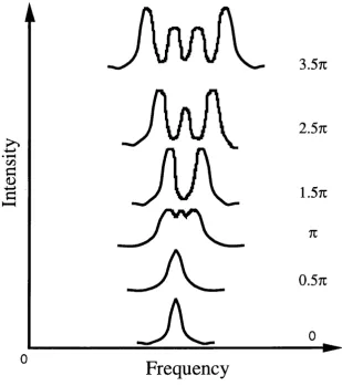
Figure 1.2 displays the calculated frequency spectra of a Gaussian pulse after propagating through a nonlinear medium as a function of light intensity . Each spectra is labelled with the maximum phase shift at the peak of the pulse. It has been shown that when the pulse is non Gaussian it will broaden slightly differently to that of the Gaussian pulse but the number of peaks in the output pulse spectrum is still dependent on the phase shift rather than the pulse shape itself. Also any asymmetry in the input pulse will result in an asymmetric spectrally broadened output pulse.
— j ; P ( t ) 1/2 V i(0)“ °o)td t (1.13)
2n
2n
= — L n J
C7) a <D
J W l
3.57c
2.5k
1.57C
K
0 .5k
0 0
Frequency
Figure 1.2. The calculated spectra for a Gaussian pulse as a function of light intensity. Each spectra is labelled with the maximum phase shift at the peak of the pulse.
The 1/e full width of the broadened spectrum Af, is related to the pulse width and the maximum phase shift by the following equation6.
Axp(fw l/e) = 1.72A(|)max/7iAf
(i.is)
1 . 4 . 2 . 3 . S elf-F o c u sin g .
Let us consider the propagation of a high intensity light pulse through a third order nonlinear material with a positive n2. In the case of a Gaussian shaped pulse the intensity of light falls gradually away from being a m axim um at the centre to a minimum at the edges. Hence, the local refractive index of the material will be greater at the centre of the light beam than at the edges. Therefore, the nonlinear medium acts as a positive lens and a light pulse will tend to focus as it propagates through the nonlinear material. Damage to the nonlinear medium can occur providing the intensity of the light pulse is high enough and if the nonlinear medium is long enough for the light to reach a focal point within the material.
1 . 4 . 2 . 4 . S o lito n s.
Soliton is the term used to describe an intensity distribution, in time or space, which remains constant as it propagates. In the following section the main types of optical soliton, relevant to this thesis, will be described.
1 . 4 . 2 . 4 . 1 . Spatial Solitons.
Spatial Solitons are self guiding or self-trapped beams that propagate w ithout changing their spatial shape. Spatial solitons are stable when diffraction is limited to one spatial dimension and have been observed in CS2 liquid waveguides7, AlGaAs semiconductor waveguides8 and in ion exchange glass waveguides9.
The propagation of a spatial soliton can be described using the nonlinear Schrodinger equation of the form:
coefficient is positive and describes a self-defocusing effect when the nonlinear material has a negative nonlinear refractive index coefficient. In a positive nonlinear m aterial spatial solitons are form ed when the effects o f diffraction are balance by self-focusing w hich tends to concentrate the energy of the light beam. The fundamental soliton can be described by the following equation: 10
E( x, z) = A n sech
f
exp
1ZA
V
2ka2
oy
(1.17)
where ao is a measure of beam width:
ka0
\jn2
(1.18)
The total soliton power in the beam is given by9:
15 n 0 2 W
P.
= ---T (1.19)n,a k
2 owhere w is the transverse mode size .For effficient two dimensional propagation w « a 0 since under these conditions the self-focusing effects are lim ited to one spatial direction. Higher order solutions exist at intensity levels of N2P t , where N is an integer.
1 . 4 . 2 . 4 . 2 . Tem poral Solitons.
equation. The mathematical treatment of these solitons can be found in many text books/papers (see Ref. 3 and 11).
1 . 4 . 2 . 4 . 3 . Bragg Solitons.
Bragg solitons are temporal-like solitons which occur at the upper band edge of the stop-band of a grating where the anomoulous group velocity dispersion is high and the grating is still transmissive. The soliton is produced by the counter balancing effect between the large anomalous dispersion associated with the periodic variation in the refractive index and the self phase modulation produced by the nonlinear medium. Bragg grating solitons have been succesfully demonstrated in optical fibres by E g g leto n 11 et al. In that experiment, the Bragg solitons produced were seen to travel at a slower speed than that of light in the medium without a grating. The typical interaction lengths for soliton formation in the fibre grating were substantially shorter than that required for soliton formation in a uniform fibre due to the large dispersion close to the stop-band.
1 . 4 . 2 . 4 . 4 . Gap solitons.
Gap solitons were first theoretically predicted by Chen and M ills13. They showed that light with a frequency within the stop band of a grating structure for certain values of intensity can be perfectly transmitting. The shape of the envelope of this transm itted wave is a hyperbolic sech function hence it is commonly known as a soliton. The soliton effectively bum s itself slowly through the stop gap by locally changing the refractive index of the material, through the nonlinearity of the material. Numerical simulations indicate that zero velocity gap solitons may be generated in a grating of finite length by illuminating both ends of the grating with two counter-propagating equally intense light beam s14. Theoretical analysis using coupled mode theory has shown that gap solitons m ay also propagate inside the grating with a group velocity controlled by selecting the waveguide parameters, which can in principle lie between c/n and 0, where n is the average effective index of the guide.
1 .5 . Desirable Attributes of a Nonlinear Optical Switch.
The desirable attributes for an efficient nonlinear switch include a high switching speed and low switching power requirem ents together in a compact form. The switching speed of a nonlinear switch is in general dependent on the origin of the nonlinearity. N onresonant nonlinear processes are a great deal faster than those of resonantly enhanced processes, which are produced as a result of material excitation caused by light absorption, and are therefore more suited to ultrafast switching applications. The power requirements of a nonlinear switch depend on the magnitude of the nonlinear coefficient, the device structure and the value of the linear and nonlinear optical losses of the material. The subject of m ulti-photon absorption together with a discussion of the nonlinear properties of AlGaAs, which make it the ideal m aterial to observe all- optical switching, are discussed in detail in chapter 2.
1 .6 . Layout of Thesis.
In this chapter, the potential of all-optical sw itches w ithin future computing and telecommunication systems and the objective of the thesis were outlined. An introduction to nonlinear optics was given and the properties of nonlinear materials were discussed.
In chapter 2 the opto-electronic properties of AlGaAs are described, including a review of its crystal structure, band structure, and its nonlinear properties.
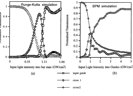
C h ap ter 4 d escribes the design, fab ricatio n and experim ental characterisation of several different nonlinear coupled waveguide arrays. The chapter begins with a brief outline of the past and future applications of nonlinear couplers followed by linear and nonlinear coupler theory. The modelling of the switching characteristics of uniform ly spaced and non-uniformly spaced couplers is described using two different numerical techniques before the fabrication process used to produce the couplers is described. Finally, the experimentally obtained switching characteristics of the couplers investigated are presented and compared to the theoretically simulated switching results.
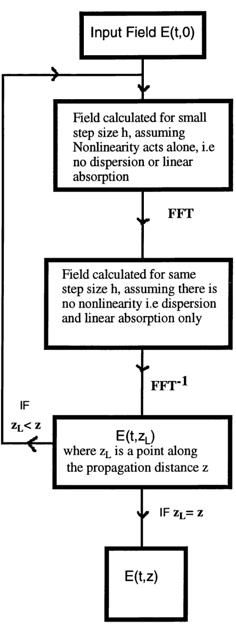
Chapter 5 describes the design, fabrication and characterisation of an all- optical switch based on the nonlinear properties of a grating waveguide filter. The chapter begins with a summary of the past, present and future applications of both linear and nonlinear grating structures followed by some basic linear and nonlinear grating theory. The nonlinear grating filter design and simulations of the switching characteristics of the grating structure using a Runge-Kutta algorithm are also given. The fabrication of the grating filter using both a holographic technique and a E-beam writing method are described and the linear characterisation of the grating filter is presented. Finally, a preliminary nonlinear result observed in a grating filter is discussed.
References.
1. C.N. Ironside, "Ultra-fast all-optical switching", Contemporary Physics, 34, pp
1-18 (1993).
2. P. A. Franken, A.E. Hill, C.W. Peters and G. Weinreich," Generation of optical
harmonics", Phys. Rev. Lett. , 7, pp 118-119 (1961). 3. R.W. Boyd, "Nonlinear optics", Academic Press, (1992).
4. D.C.Hutchings, "Applied nonlinear optics", University of Glasgow course notes,
1997.
5. A.C. Walker, "A comparison of optically nonlinear phenomena in the
context of optical information processing", Optical Computing and processing
X PP 91-106 (1991).
6. R. Stolen and C. Lin,"Self-phase-modulation in silica optical fibers", Phys. Rev.
A, 17, pp 1448-1453 (1978).
7. J.S. Aitchison, A.M. Weiner, Y. Silberberg, D.E. Leaird, M.K. Oliver, J.L.
Jackel and P.W.E. Smith, "Experimental observation of spatial soliton
interactions", Opt. L ett., 16, pp 16-17 (1990).
8. J.S. Aitchison, K. Al-Hemyari, C.N. Ironside, R.S. Grant and W. Sibbett,
" Observation of spatial solitons in AlGaAs waveguides", Electron. Lett. , 28, pp 1879-1880 (1992).
9. J.S. Aitchison, A.M. Weiner, Y. Silberberg, M.K. Oliver, J.L. Jackel, D.E.
Leaird, E.M. Vogel and P.W.E. Smith, "Observation of spatial optical solitons in
a nonlinear glass waveguide", Opt. Lett. , 15, pp 471-473 (1990).
10. Y.Silberberg,"Self-induced waveguides:spatial optical solitons", Anisotropic and
nonlinear optical waveguides, Elsevier Science Publications, pp 143-157 (1992).
11. H.A. Haus and W.S. Wong, "Solitons in optical communications", Rev. of
mod. phys. , 68, pp 423-444 (1996).
12. B.J. Eggleton, R.E. Slusher, C. Martijn de Sterke, P.A. Krug, J.E. Sipe,
"Bragg grating solitons", Phys. Rev. Lett. , 58, pp 1627-1630 (1996).
13. W. Chen and D.L. Mills," Gap solitons and the nonlinear optical response of
superlattice", Phys. Rev. Lett. , 58, pp 160-163 ( 1992).
14. A.B. Aceves, C.De Angelis, S. Wabnitz," Self-induced transparency solitons in
Chapter 2
The Nonlinear Optical Properties of
AlGaAs.
Introduction.
AlGaAs has become a popular material for the construction of nonlinear devices for several reasons. First of all, the value of 112 in AlGaAs is
approximately three orders of magnitude greater than that of silica. This means that AlGaAs devices are typically a few centimetres in length and are therefore more compact than comparable fibre devices, which can be tens of meters long. In addition, they can potentially be used for monolithic integration with other opto-electronic/electronic components. High purity, low defect materials can be manufactured, which can be selectively doped with great accuracy. The m ature fabrication technology allows a range of relatively com plex devices to be constructed. Another advantage of using AlGaAs is that the index of refraction and bandgap of the compound semiconductor can be easily changed by varying the A1 content to suit the operational characteristics of the particular device. Thus AlGaAs provides an ideal test system for investigating nonlinear optical effects.
2 .1 .1 . The Crystal Structure o f AlGaAs.
The crystal structure of GaAs is shown in fig. 2.1. GaAs has a "zinc blende" structure consisting of 2 inter-penetrating, face-centred cubic lattices, one composed of Ga atoms and the other of As atoms. The cubic unit cell contains 4 atoms each of gallium and arsenic. Each atom is tetrahedraly surrounded by four atoms of the opposite species. The length of each side, the lattice constant, a, is 0.565 nm at 300 K. The crystal does not have a centre of symmetry and can therefore be used to produced second order as well as third order nonlinear effects. The semiconductor AlGaAs is produced by replacing some of the Ga atoms with A1 atoms in the crystal structure. The lattice constants of GaAs and AlGaAs differ by less than 0.15%. Therefore it is possible to grow layers of AlxGai_xAs, where x denotes the percentages of aluminium in the layer, on top of one another without introducing significant stress.
(001)
(010)
(100)
Figure 2.1. The crystal structure of GaAs.
By altering the fraction x in the compound AlxGai_xAs, the refractive index of the material can vary from 2.92 for pure AlAs up to 3.43 for GaAs at a wavelength of 1.5 pm. The band gap of the alloy varies from
2 .1 .2 . Fabrication of AlGaAs.
Molecular-beam epitaxy and vapour-phase epitaxy are two of the common methods which are used in the production of high quality epitaxial semiconductors2. Epitaxial growth involves the crystalline growth of thin layers of the semiconductor material on a crystalline substrate base. The thickness, doping and composition of the layers are all well controlled in these processes. In this study, the AlGaAs wafers had been fabricated using molecular beam epitaxy (MBE). In this section the basics of the MBE technique are described.
electron gun
Ga
Knudsen cell
molecular beam
As
substrate
heated rotating substrate holder shutter
screen for viewing
(RHEED)
Figure 2.2. Sim plified schematic of the MBE process. (Ref. 10).
2 .2 . Band structure of III-V Compound Sem iconductors.
Figure 2.3 shows the four band Kane model4 which is commonly used to describe the band structure of III-V com pound sem iconductors. The model consists of one doubly-degenerate conduction band and three doubly-degenerate valence bands (light hole, heavy hole, split off). GaAs has eight outer electrons and of these eight, two electrons fill S-like states, referred to as the light hole band, where each electron has a total angular momentum of 1/2 .The other six electrons fill the P-like states and have a total angular momentum of 3/2 and are referred to as the heavy hole band. Fundam ental optical absorption occurs between the heavy/light hole valence bands and the first electron level in the conduction band. At higher photon energies transitions involving the lower split off valence band, which is seperated from the light and heavy hole bands by 0.34 eV due to spin-orbit splitting, take place.
o f the conduction band changes its energy but not its m o m en tu m . This
leads to a sharp band-edge. In contrast, for indirect b an d gap m aterials
such as silicon and g e rm a n iu m the transition o f an e lectro n from the
valence to the conduction band involves a change in both the energy and
m om entum . The additional m o m en tu m is provided by a lattice vibrational
phonon.
conduction band
valence band electrons
laser light
vwwvv
Figure 2.3. Band structure of III-V com pound sem iconductors
as given by the Kane model.
2 .3 . Types of N o n lin e aritie s in D irect G ap S em ico n d u cto rs.
The m agnitude and origin of
r
\2 in com pound sem iconductors depends on the wavelength of the incident light beam in relation to the position of theband-gap o f the sem iconductor. In general the optical nonlinearities fall
2 .3 .1 . R esonant N onlinearities.
The resonant nonlinearities occur at optical wavelengths close to the linear bandgap absorption edge. There are several different mechanisms which are responsible for the nonlinear response including band filling5, excitonic effects6, plasma7 and opto-thermal effects8.
In general these processes involve the absorption of light, resulting in the establishm ent of real excited populations w hich through the Kramers-Kronig relation, as discussed in section 2.4, leads to a change in the refractive index of the material. Such effects produce large optical nonlinearities. However, the response times of these effects, which are governed by the relaxation time of the electrons from the excited states, are slow ( about a few nanoseconds ). The speed can be improved by applying an electric field to remove the carriers. However, the absorption of light results in a low throughput (1 0 %) and undesirable therm al effects. Devices based on resonantly enhanced nonlinearities are also very wavelength sensitive and can suffer from saturation effects. On the whole this type of nonlinearity is not suitable for ultrafast switching applications.
2 .3 .2 . N on-R esonant N onlinearities.
2 .4 . M easurem ent of the Nonlinear C oefficient.
2 .4 .1 . K ram ers-K ronig R elation.
The Kramers-Kronig (K-K) formalism is a common dispersion relation equation in linear optics which relates the refractive index, n, of a m aterial to the absorption coefficient, a , over all frequencies, Q and can be expressed by9:
The K-K formalism can be modified to calculate a change in refractive index, An, from a change in absorption, A a, due to some external perturbation, For exam ple in a resonant nonlinear process the material excitation can be regarded as the perturbation. The change in refractive index is derived by applying the relation (2.1) to a system, before and after the perturbation and then taking the difference between the two cases. The change in refractive index can be expressed as:9
This expression has been used in the past to calculate the dispersion of the nonlinear refraction coefficient, n2, since the index change induced by the local intensity, I, is related to n2 by the following equation:
The scaling and dispersion of n2 in a semiconductor crystal over the entire spectral range for photon energies below the fundamental absorption edge has been carried out using the K-K formalism. The calculations showed that in the half-band gap spectral region there is an enhancement in the size of n2 , and that the magnitude of n2 depends on Eg 4 . In that analysis a two-parabolic band model was used and two-photon absorption and the ac stark shift w ere assum ed to be the dom inant nonlinear absorption processes10.
c °;(x(£2)d&2
K I Q
2- C O
2(
2
.1
)2 .4 .2 . Higher Band M odels.
Studies have shown that the magnitude of 112 depends on the polarisation of
the light and also on the orientation of the crystal. In order to study the effects of the polarisation on the nonlinear refraction coefficient as well as its anisotropy, the K-K method for calculating the dispersion of ri2 has
recently been superseded by methods based on calculating n2 directly from
the real part of the nonlinear susceptibility using higher band structure models.
The 4 band Kane model, shown in fig. 2.3 has been used to obtain the dispersion of the nonlinear refractive index of direct-gap semiconductors. The standard expression for n2 obtained using perturbation theory is given by
3
n 2(® ) = 7 - — r R e jclL (-< 0 , <*>,©,) (2 4)
4 e
0
cn
0
It was found using this model that %*3W x can be expressed as:
< 2 5 >
where
f^oyE
, A jE j
is a dimensionless spectral function and A is the energy difference between the upper valence band and the split off energy band as illustrated in fig. 2.2. Ep is the Kane momentum energy given by:2m P
2
E p = —- - — « 20 eV (
2
.
6
)
where P is the Kane momentum parameter and m is electron mass.
in additon the effects of the crystallographic orientation on the magnitude of n2 have been studied using this higher band model. Dichroism produces different values of n2 for linear and circular polarised light. It was seen from this analysis that:
n
2(T E )> n
2(TM)
Figure 2.4 shows the recent experimentally measured dispersion of the nonlinear refraction coefficient for Alo.1sG ao.8 2As for TE and TM polarisation, obtained by measuring the self-phase modulation of a light pulse propagating through the m aterial11.The sam ples used in this experim ent consisted of 5 jLtm wide strip loaded AlGaAs waveguides etched 1.35-1.45 pm deep into the top cladding layer of an AlGaAs wafer with the follow ing structure: The guiding region was com posed of a 1.5pm thick Alo.1sGao.8 2As layer.The upper cladding was a 1.5pm thick A lo .2 4G a o .7 6As layer and the low er cladding was a 4 p m thick Alo.2 4Gao.7 6As layer.
2 -
--0
0 1. 8- A
(N
a
1. 6 -0CO
0
1.4-(N
a
1.
21
-0.8
1480 1520 1560 1600 1640
wavelength (nm)
Figure 2.4. The measured dispersion of n2 for TE (solid dots) and TM (solid
2.5. M ulti-Photon A bsorption in AlG aA s Guides.
In this study switching configurations composed of AlGaAs waveguides are investigated. The loss experienced by a light field propagating through the AlGaAs guide can be expressed as13:
— 1
= - a l - a
2
I
2
- a
3
I
3
(2.7)
dz
2 3where I is the light intensity, a , is the linear absorption coefficient and 0C2 and (X3 are the two-photon and three-photon absorption coefficients respectively. At low light intensities linear loss is the dom inant loss mechanism. The linear loss is dependent on the energy of the photons, scattering and thermal effects. If L is the length of the guide then the intensity of the light propagated through guide is related to the incident light intensity, Io into the guide by the following equation:
I = I
0e_aL
(2.8)
When the energy of a light photon Eph given by:
Eph
=h
CO (2.9)is larger than the bang-gap energy, Eg, of the semiconductor, a direct inter-band transition can occur. This means that a single photon is absorbed and results in the transition of an electron from the valence band to the conduction band. At photon energies well below the band-gap energies i.e. at half-the band gap direct inter-band transitions are not possible and so the linear loss is mainly due to scattering losses and thermal effects. Linear loss in AlGaAs operating in the half-band gap spectral region is discussed further in chapter 3.
2 .5 .1 . T w o-Photon A bsorption.
When the energy of the photon is below the band-gap energy in the range expressed by:
1
—E„ < Tico <E„
2
8
8
then the transition of an electron from the valence band to the conduction band requires the absorption of two-photons. Two-photon absorption is related to the imaginary part of the third order nonlinear susceptibility as discussed in section 1.4 and is dependent on the intensity of the light as expressed in (1.15).
The dispersion of the two-photon absorption coefficient for AlGaAs operating below the fundamental band gap has been analysed using the Kane band model. It was found that the two-photon absorption coefficient can be expressed as:5
a
= K
2 - 2t - 3 (
2
.10
)where Ep is the Kane momentum energy and K is a material independent constant given by:
K =
2
k
e
3100 cmGW^eV^2
(
2
.
11
)
5 Vm oc
where e,mo and c are the charge,free electron mass and the speed of light respectivley.
To observe efficient switching within a nonlinear device, such as a nonlinear directional coupler in the presence of two photon absorption, the following condition must be met14:
a
2a
2IcLc
<
0.5
(2.13)
where Ic is the critical switching intensity, a2 represents the overlap integral over the mode profiles in the waveguide for the third order nonlinearity and Lc is the half beat coupling length.
1.4
1.2
1
5
0.8
1
~ 0.6 a
0.4
0.2
0
1490 1500 1510 1520 1530 1540 1550 1560
Wavelength (nm)
Figure 2.5. The experimentally measured values of ax as a function of
wavelength for TE (solid circles) and TM (open circles) light for 5pm wide strip loaded AlGaAs waveguides.
The two photon absorption coefficient exhibits optical polarisation dependence due to the fact that the third order susceptibility tensor contains off-diagonal elements.
2 .5 .2 . Three Photon A bsorption.
Three photon absorption (3PA) is a fifth order absorption process involving the simultaneous absorption of three photons. Three photon absorption occurs when the energy of the photons are below the half-band gap spectral region. The value of the three photon absorption coefficient, 0C3, for AlGaAs operating below the band-gap has been defined as15:
n—i—i—i—|—i—i i—I | i i—i-T—|—i—i—n —I—i—i—i i—I—i i i i r—i i r
$ TE
o TM
o
$
a . =
310
V
2
8
r 3 -*-2
71
U c J
r E
p V
( f. ^ \ 2 3 ^ - 1
E.
J
n
3E
7U 0E g
( 4- \ 93
—
E . y
(2.14)
The criterion for nonlinear switching in the presence of three photon absorption requires t h a t 14:
I*a
3a
3Lc < l
(2.15)where is the overlap integral over the mode profiles in the waveguides for the fifth-order nonlinearity.
Figure 2.6 shows the theoretically calculated dispersion of the three photon absorption coefficient for different concentrations of Al11.
0.35
18%A1 - - 19%Al 20% Al
_ 0.3
<N
£
5 0.25
a
o 0.2
0.15
3
01
£
^ 0.052.2 2.4
1.2 1.4 1.6 1.8 2
1
wavelength (pm)
This graph shows that the three photon absorption coefficient is at a maximum at a wavelength of ~ 2.1 pm. However, in the half band gap region the 3PA coefficient is still large enough to affect the switching efficiency of an all-optical switch. Figure 2.7 shows the recent experimentally measured dispersion of 0C3 calculated using the AlGaAs waveguides as described in section 2.4.2. These experimental results agree well with the theoretically predicted dispersion of 0C3.
0.16
0.12
£
CO
J , 0.08
s'
0.04
1450 1500 1550 1600 1650 1700
wavelength (nm)
Figure 2.7 Experimental values of 0C3 as a function of wavelength.
2.6. C onclusions of Chapter.
References.
1. A. Villeneuve, "Optical nonlinearities and applications of semiconductors near half
the band gap", Ph. D. Thesis , University of Arizona (1992).
2. E.F. Scubert, "Dopings in ni-V semiconductors", Cambridge University Press, - chp.4, pp 137-164 (1993).
3. J.H. Davies, "Heterostructures", University of Glasgow lecture notes, pp 68-96
(1994).
4. E.O. K ane," Band structure of Indium Antimonide", J. Phys. Chem. Solids, 1,
pp 249-261 (1957).
5. A. Villeneuve, "Optical nonlinearities and applications of semiconductors near half
the band gap", Ph. D Thesis , University of Arizona, Chp. 2 (1992).
6. F.R. Laughton, "Nonresonant optical nonlinearities in GaAs/AlGaAs multiple
quantum well waveguides", Ph. D Thesis, University of Glasgow, chp.2 (1991).
7. D.A.B. Miller, S.D. Smith and B.S. Wherrett, "The microscopic mechanism of
third order nonlinearity in InSb", Opt. Commun. , 35, pp 221-224 (1985).
8. M.C. Gabriel, H.A. Haus and E.P. Ippen, "Thermal index changes by optical
absorption in group III-V semiconductor waveguides", J. Lightwave Tech., 4, pp 1482-1493 (1986).
9. D.C. Hutchings, M. Shiek-Bahae, D.J. Hagan and E.W. Van Stryland,
"Kramers-Kronig relations in nonlinear optics", Opt. and Quant. E lec., 24, pp 1-30 (1992).
10. D.C. Hutchings and B.S. Wherret, "Theory of the dipersion of ultrafast nonlinear refraction in zinc-blende semiconductors below the band-edge", Phys. Rev.
,50, pp 4622-4630 (1994).
11. J.S. Aitchison, D.C. Hutchings, J.U. Kang, G.I. Stegeman and A. Villeneuve,
"The nonlinear optical properties of AlGaAs at the half band gap", IEEE J. of
Quant. Elec. , 33, pp 341-347 (1997).
12. D.C. Hutchings, B.S. Wherret, "Theory of the anisotropy of ultrafast nonlinear
refraction in zinc-blende semiconductors", Phys. Rev. B, 52, pp 8150-8159 (1995).
13. J.U. Kang, A. Villeneuve, M. Sheik-Bahae, G.I. Stegeman, K. Al-Hemyari, J.S.
Aitchison and C.N. Ironside, "Limitation due to three-photon absorption on the
useful spectral range for nonlinear optics in AlGaAs below halfband gap.", Appl.
Phy. Lett. , 65 , ppl47-149 (1994).
14. C.C. Yang, A. Villeneuve and G.I. Stegeman, "Effects of three-photon absorption
on nonlinear directional coupling", Opt. Lett. 17, pp 710-712 (1992).
15. B.S. Wherrett," Scaling rules for multiphoton interband absorption in
CHAPTER 3
Semiconductor Waveguide Design,
Fabrication and Characterisation.
Introduction.
Semiconductor waveguides are attractive elements for the implementation of a range of all-optical switching devices since high optical power densities can be m aintained over long interaction lengths. To date ultrafast switching has successfully been dem onstrated in nonlinear directional couplers1, M ach-Zender interferom eters2 and X-junction devices3. In this chapter the design, fabrication and characterisation of sem iconductor w aveguides for ultrafast sw itching effects will be discussed.
3 .1 . Properties o f Sem iconductor O ptical W aveguides.
Semiconductor waveguides are ideal elements for the construction of nonlinear, all-optical devices. The main attributes of such waveguides will be outlined below.
3 .1 .1 .1 . Optim um Geom etry.
N onresonant nonlinearities are sm all com pared to their resonant counterparts, i.e. n2 for AlGaAs operating in the half band gap region is approximately l x l O13 W /cm 2. Therefore, to observe ultrafast all-optical switching effects the nonlinear phase shift required must be accumulated over a large propagation distance. Optical w aveguides provide the optimum interaction geometry, since they allow high optical intensities to be maintained over long propagation lengths. The waveguides enable diffractionless propagation in one, or two, transverse directions. By contrast in a non-waveguide geometry, diffraction limits the length over which the high optical intensity can be maintained. In addition, the index of refraction of compound semiconductors such as AlGaAs can be easily altered, as discussed in chapter 2. The waveguides can then be constructed from an AlGaAs wafer composed of different layers of AlGaAs grown one on top of another.
3 .1 .2 .1 Compactness and Potential for M onolithic In tegration .
3 .1 .1 .3 . M ature Fabrication Technology.
Semiconductors have a mature, advanced fabrication technology which allows a wide range of complex integrated devices to be fabricated. Another advantage of semiconductor waveguides is that the scribe and cleave technique used for end facet preparation in these guides is simple as opposed to the cut and polish method used in other nonlinear materials such as LiNb0 3 and glass. The resulting waveguides can also have very low propagation losses.
3.2. Basic Optical W aveguide Theory.
3 .2 .1 . Snell's Law and Total Internal R eflection.
The propagation of light in a dielectric waveguide can be described in terms of geometric optics. This approach allows the m ajor waveguide properties to be defined. However, it should be noted that this approach is approximate and a full description requires the application of Maxwell's equations with the appropriate boundary conditions. W hen a light ray strikes the boundary between two transparent m edia at an angle 0 , a fraction of the light will be reflected while the rest of the light is transm itted through the interface at an angle known as the refracted angle. Figure 3.1 shows an incident light ray i, incident on an interface between two m edia and the resulting reflected, r, and transm itted fraction, t, of the ray. The relationship between the incident and transmitted ray is given by the law of refraction commonly known as Snell's laws, as stated below5:
rij sinGj = n 2 s i n 0 t
(3.1)
Figure 3.1. Shows the incident, reflected and transm itted rays at an interface
boundary betw een two different m edia w ith refractive indices ni and n2 .
W hen light travels from a m edium of index ni, to a low er index region
n2
there is a specific angle o f incidence, 0 C, for w hich the refracted ray will propagate parallel to this surface. This is called the critical angle. If the incident angle is greater than 0 C the light is totally reflected by theinterface.
From Snell's law 0c is given by;
0 = sin
- 1(
n 23
lnJ
(3.2)An important feature of the total internal reflection process is that when a
light ray is reflected by an interface the ray will penetrate slightly into
3 . 2 . 2 P ro p a g a tio n o f L ig h t in a D ie le ctr ic S lab W a v e g u i d e .
In this section ray optics will be used to describe the propagation of an
EM w a v e in a slab w av eg u id e. T h e slab w a v e g u id e co n sists o f a
tra n s p a re n t d ielectric m aterial o f high re fra c tiv e in d ex sa n d w ich e d
b etw een two layers o f dielectric m aterial w ith low er refractive index.
Figure 3.2 illustrates the path o f a ray as it p ropagates through such a
dielectric slab. Propagation of light in a slab dielectric m edium is similar
to that o f light travelling through an optical fibre.
n l
n3
Figure 3.2. illustrates the path of a ray of light travelling w ith in the guiding region of a dielectric slab .
T he con d itio ns w hich m ust be satisfied to a ch iev e guid in g w ithin a
dielectric slab can be sum m arised as follows :
1 . The refractive index of the guiding m edium m ust be greater than those of the adjacent layers, i .e . n2> n i, n^.
2 . The angle 0 m must be greater than the critical angle
0c-3. For a guided wave the transverse field m ust form a standing wave.
If not then it will be a travelling wave and the field will dissipate
power. This means that the total phase change experienced by a
integral number of 2k. This rule can be expressed by the
following equation:
where is the polarisation sensitive, phase change experienced by the ray when reflected from the index boundaries and Xx is the wavelength of the transverse Ex field.
M ode cut off occurs at low incident frequencies, when the angle of incidence is low enough to inhibit total internal reflection, causing the light to escape from the guiding region into the surrounding medium. It can be shown that the mode angle 0m , of each mode propagating in the guide is given by:
where Xq is the wavelength of the light in vacuum.
3 .2 .3 . M axw ell’s E quations.
Since light is an electromagnetic field, the wave characteristics of modes propagating within the simple slab guide can also be determined using M axwell’s equations. These equations are mathematical formulae which describe the propagation of electromagnetic fields in materials, were the wavelength is much bigger than the atomic, or molecular dimensions. In this section the basics mode equations are discussed. For com plete derivation of the mode solutions for the slab guide see ref. 6 .
Assuming the waveguide medium is nonconductive, has no charges and is isotropic the equations which described the electric and magnetic fields within the slab guide are as follows:
C O S0m (3.4)
2ndn
2V » |lH = 0
(3.5b)Y7 17
VxE
d U= — |LL|LL0 — (3.5c)
at
y7 t t 5 E
VxH
= £ £ 0 — (3.5d)at
where E and H are the electric and magnetic field strengths, p,o and ji are the permeability of free space and of the material respectively, while £o and £ are the perm ittivity of free space and the perm ittivity of the material respectively. By taking the curl of equation 3.5c the following equation is obtained.
VxVxE
=V (V .E )- V2E
= - |4 i0 9 ( V >x H ) (3.6)at
Substituting equation 3.5d into equation 3.6 gives:
V 2E =
|Li|u
0
e e
0
a 2E = ( n Y a ^ E
9t2
v c y 5t2
(3.7)Assuming the wave is monochromatic, travelling in the z direction and is confined only in the x direction, the electric field E and magnetic field H can be expressed by the following :
E = E (x ,y )e i<<aH3z>
H = H (x ,y )e i<fi>H5z)
(3.8)
Combining equation (3.8) and (3.7) gives:
where ko=27t/^o.
In a one dimensional slab waveguide where 5/5y=0, two types of solution exist for the equation 3.9 depending on the polarisation of the light. The first is known as the transverse electric, or (TE) modes, these are composed of Ey, Hx, Hz components only. The second is known as the transverse magnetic fields or (TM) which are com posed of the Hy, Ex and Ez components. Using equation 3.9 the TE fields propagating within the three separate regions of the slab guide can be described by the following equation.
The TE and TM guided mode solutions can be obtained by solving equations 3.10 and 3.11 with suitable the boundary conditions. At the interface for TE modes, Ey and 8Ey/5x must be continuous. Likewise for TM modes, Hy and 5Hy/5x must be continuous. It should be noted that as x tends to plus or minus infinity then Ey or Hy will tend to zero.
Figure 3.3 illustrates the different type of fields which propagate within the 3 regions which make up the slab guide. As shown in figure 3.3 the guided waves of the slab obey the following condition kon3 <P < kon2 and correspond to a field which varies in a sinusoidal m anner within the guiding layer and exponentially decays in the lower index regions.
where i= l, 2, 3. Similarly the TM modes are described by:
0 < P < K 0 n, K0n , < P < K 0n 3 < p < K()n2 p > K0n 2
I
I
/
\
I
Figure 3.3. Illustrates the field characteristics in each layer of the slab guide
for various values of propagation constant.
3.3 O p tical W av eg u id e D esig n .
In the w aveguide design process, the im portant factors w hich m ust be
taken into account include, the operating w avelength, g eo m etry o f the
waveguide structure, losses within the structure and w afer composition.
In this research single m ode A lG aA s w av eg u id es op eratin g below the
h alf-band gap and within the low loss com m u n icatio n s w in d o w at 1.55
p m were fabricated. In this spectral region the detrim ental effects due to
3 . 3 . 1 . W a v e g u id e G e o m e tr ie s .
In section 3.2 we looked at the sim ple slab g u id e w ere the light is
confined in one transverse dimension. In practical w av eg u id e structures
light must be confined is two dimensions. Vertical confinem ent is usually
achieved by refractive index differences betw een the layers which m ake
up the w afer. In the lateral directio n , op tical c o n fin e m e n t can be
introduced in several ways including carrier indiffusion and superlattice
disordering. How ever, the m ost frequently used m eth o d is by etching a
rib into the m aterial layers. T he c o n fin em en t is then due to effective
index differences betw een the etched and u n etch ed regions. Figure 3.4
b e lo w illu stra te s fo u r ty p es o f rib w a v e g u id e s tru c tu re s that are
com m only used.
a] strip guide b] embedded strip guide
c] ridge waveguide d] strip loaded guide
Figure 3.4. Illu stratio n of the v arious m ethod of lateral co n fin em en t by
using various types of rib w aveguide geom etries used.
In this research strip loaded guides w ere fabricated. This structure was
chosen as both coupled w aveguides, grating structures on ridge guides
and curved w aveguides can be fabricated. T he guiding characteristics of
the guide can be controlled by varying the height, or w idth, o f the rib
structure. In general deeply etch ed ridges p ro d u ce stro n g ly c o n fin ed
m odes suitable for the production o f curved structures. S h allo w er ribs
form w eaker guides which are suitable in coupled w aveguide and grating
3 .3 .2 . Sources of Linear Loss w ithin Sem iconductor W avegu id es.
Low loss waveguides are essential for optical guided wave applications. Therefore, potential sources of loss within optical waveguides and the ways in which these loss mechanisms can be reduced are im portant factors which need to be considered when designing waveguides.
Linear propagation losses within AlGaAs waveguides operating below half the band gap are caused by a combination of absorption, scattering and leakage7. In this section we look at each source of loss in turn and discuss the methods em ployed in this research to reduce these loss mechanisms.
3 .3 .2 .1 . Scattering losses are caused by epilayer and rib sidewall roughness and also scattering from imperfections. In this research the AlGaAs wafer used to fabricate the waveguides was grown by MBE, which results in high quality layers with minimum scattering. Losses due to sidewall roughness have been shown to depend on the rib width and also on (Aneff)2, where Aneff is the effective index differences between the etched and unetched regions of the waveguide. The smaller the rib width and deeper the rib is etched, the greater the scattering loss in the optical waveguides. With this in mind the width of the guides in this research were chosen to be 4 (im wide. In addition, the guides were fabricated using an up to date photolithographic and dry etch process which has been shown to produce guides with excellent surface/sidewall definition8.
3 .3 .2 .2 . Leakage of light from the guiding region into the substrate layer occurs when the substrate m aterial has a sim ilar, or higher refractive index to the guiding layer. This loss decreases exponentially with the cladding thickness. Therefore, loss due to leakage can be reduced by growing a thick lower cladding layer.