AN IMPROVED DESIGN OF A
MULTIPLIER USING REVERSIBLE
LOGIC GATES
H.R.BHAGYALAKSHMI
Department of Electronics and Communications, BMS College of Engineering , Bangalore, India
M.K.VENKATESHA
Department of Electronics and Communications, RNS Institute of technology,, Bangalore, India
Abstract:
Reversible logic gates are very much in demand for the future computing technologies as they are known to produce zero power dissipation under ideal conditions. This paper proposes an improved design of a multiplier using reversible logic gates. Multipliers are very essential for the construction of various computational units of a quantum computer. The quantum cost of a reversible logic circuit can be minimized by reducing the number of reversible logic gates. For this two 4*4 reversible logic gates called a DPG gate and a BVF gate are used.
Keywords: Reversible logic circuits; quantum computing; Nanotechnology.
1. Introduction
Reversible logic has received great attention in the recent years due to their ability to reduce the power dissipation which is the main requirement in low power VLSI design. Quantum computers are constructed using reversible logic circuits. It has wide applications in low power CMOS and Optical information processing, DNA computing, quantum computation and nanotechnology. In 1960 R.Landauer demonstrated that high technology circuits and systems constructed using irreversible hardware result in energy dissipation due to information loss [1]. According to Landauer’s principle, the loss of one bit of information dissipates KTln2 joules of energy where K is the Boltzmann’s constant and T is the absolute temperature at which the operation is performed [1]. The heat generated due to the loss of one bit of information is very small at room temperature but when the number of bits is more as in the case of high speed computational works the heat dissipated by them will be so large that it affects the performance and results in the reduction of lifetime of the components. In 1973, Bennett, showed that one can avoid KTln2 joules of energy dissipation constructing circuits using reversible logic gates [2].
2. Reversible logic gates
A reversible logic gate is an n-input n-output logic device with one-to-one mapping. This helps to determine the outputs from the inputs and also the inputs can be uniquely recovered from the outputs. Also in the synthesis of reversible circuits direct out is not allowed as one–to-many concept is not reversible. However fan-out in reversible circuits is achieved using additional gates. A reversible circuit should be designed using minimum number of reversible logic gates. From the point of view of reversible circuit design, there are many parameters for determining the complexity and performance of circuits [3, 4 and 18].
The number of Reversible gates (N): The number of reversible gates used in circuit.
The number of constant inputs (CI): This refers to the number of inputs that are to be maintained constant at either 0 or 1 in order to synthesize the given logical function.
The number of garbage outputs (GO): This refers to the number of unused outputs present in a reversible logic circuit. One cannot avoid the garbage outputs as these are very essential to achieve reversibility.
play an important role in computational operation using computers. There are many arithmetic operations which are performed, on a computer ALU, through the use of multipliers. Design and implementation of digital circuits using reversible logic has attracted popularity to gain entry into the future computing technology
.
This paper is organized as follows: Section 2 gives the brief introduction of the reversible logic gates required for the present work. Section 3 describes the design of multiplier circuit and the implementation of the proposed multiplier circuit using new reversible gates. Section 4 gives the results and discussions and the comparative study of different designs with the proposed design. Finally Section 5 concludes with a scope for further research.
2.1. Basic reversible logic gates
2.1.1 Feynman Gate: Fig.1 shows a 2*2 Feynman gate [6]. The input vector is I (A, B) and the output vector is O (P, Q). The outputs are defined by P=A, Q=AْB. Quantum cost of a Feynman gate is 1.
Fig 1: Feynman gate
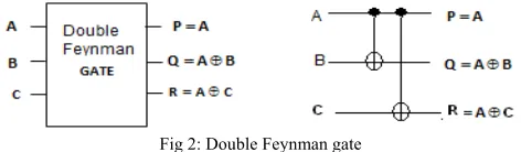
2.1.2 Double Feynman Gate (F2G):Fig.2 shows a 3*3 Double Feynman gate [7].The input vector is I (A, B, C) and the output vector is O (P, Q, R). The outputs are defined by P = A, Q=AْB, R=AْC. Quantum cost of double Feynman gate is 2.
Fig 2: Double Feynman gate
2.1.3 Toffoli Gate: Fig 3 shows a 3*3 Toffoli gate [3] The input vector is I(A, B, C) and the output vector is O(P,Q,R). The outputs are defined by P=A, Q=B, R=ABْC. Quantum cost of a Toffoli gate is 5.
Fig 3: Toffoli gate
Fig 4: 3*3 Fredkin gate
2.1.5 BVF gate: Fig.5 shows a 4 * 4 BVF gate. This is a reversible double XOR gate and can be used for duplication of the required inputs to meet the fan-out requirements. The input vector is I(A,B,C,D) , the output vector is O(P,Q,R,S) and the output is defined by P = A, Q = AْB, R = C and S = CْD. Quantum cost of a BVF gate is 2. In the proposed design this gate is used to copy the operand bits and it is shown that the number of gates required to copy is reduced by 50% with same quantum cost.
Fig 5: BVF gate
The existing 4*4 gates namely MKG [13], TSG [14], HNG [15] and PFAG[16] can be individually used as an adder. Of all this HNG gate has least hardware complexity. It is shown that using the proposed DPG gate the quantum cost of the multiplier is kept to the minimum value and at the same time it is more flexible as it can be used either as a half adder or as a full adder.
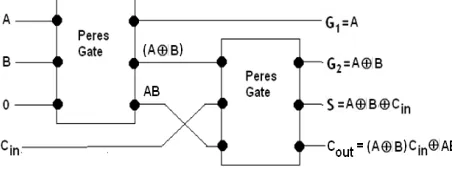
2.1.6 Peres Gate: Fig 6 shows a 3*3 Peres gate [10]. The input vector is I (A, B, C) and the output vector is O (P, Q, R). The output is defined by P = A, Q = AْB and R=ABْC. Quantum cost of a Peres gate is 4. In the proposed design Peres gate is used because of its lowest quantum cost.
Fig 6: Peres gate
A full-adder using two Peres gates is as shown in fig 7. The quantum realization of this shows that its quantum cost is 8 two Peres gates are used.
Fig 7: Full adder using two Peres gates
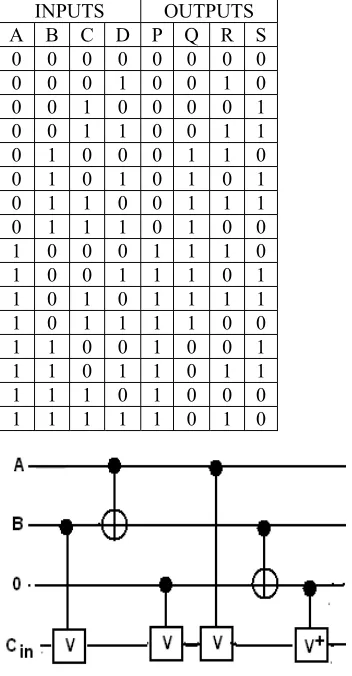
Fig 8: DPG gate Table-1: Truth table of DPG gate
INPUTS OUTPUTS A B C D P Q R S
0 0 0 0 0 0 0 0 0 0 0 1 0 0 1 0 0 0 1 0 0 0 0 1 0 0 1 1 0 0 1 1 0 1 0 0 0 1 1 0 0 1 0 1 0 1 0 1 0 1 1 0 0 1 1 1 0 1 1 1 0 1 0 0 1 0 0 0 1 1 1 0 1 0 0 1 1 1 0 1 1 0 1 0 1 1 1 1 1 0 1 1 1 1 0 0 1 1 0 0 1 0 0 1 1 1 0 1 1 0 1 1 1 1 1 0 1 0 0 0 1 1 1 1 1 0 1 0
Fig 9: DPG gate as full adder
3. Design of Reversible Multiplier
The design of the proposed multiplier uses parallel multiplier is done using two steps. Part I: Partial Product Generation (PPG)
Part II: Multi-Operand Addition (MOA)
Fig 10: The operation of the 4×4 parallel multiplier
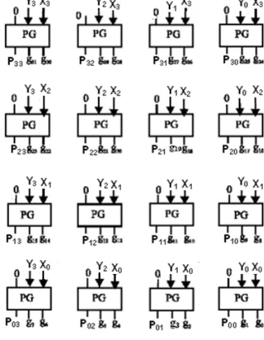
3.1 Partial Product Generation
Partial products can be generated in parallel using 16 Peres gates as shown in Fig. 11. This uses 16 Peres gates and is a better circuit as it has less hardware complexity and quantum cost compared to other gates [13].
Fig 11: Partial Product generation circuit using Peres gates
Fig 12: Fan-out circuit to duplicate the operand bits
3.2 Multi-operand Addition (MOA)
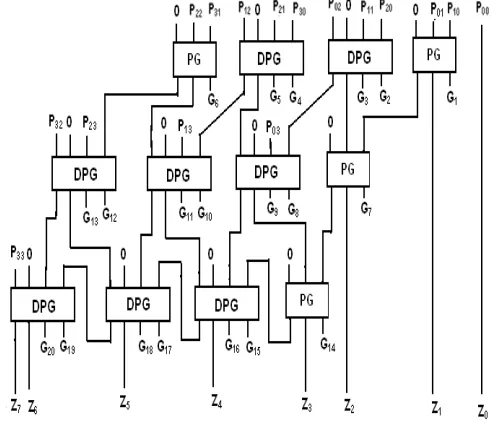
As proposed in [12], to implement an n operand addition circuit part a carry save adder (CSA) is used. The CSA tree reduces the four operands to two. Thereafter, a Carry Propagating Adder (CPA) adds these two operands and produces the final 8-bit product. The proposed four operand adder shown in Fig 13 uses DPG gate as a reversible full adder and Peres gate as half adder.
Fig. 13: Four-operand Addition (Block diagram)
The proposed reversible multiplier circuit uses 8 reversible DPG gates and 4 Peres gates. The peres gate half adder has quantum cost of 4 and the DPG adder has quantum cost of 6 and the total quantum cost of this circuit is 64.
4 Results and Discussion
Comparison of different designs is done separately for both the parts of each multiplier.
The quantum cost of a PFAG [16] is shown as 8.The quantum costs of HNG, MKG and TSG is declared as ‘unknown’ in [16] but it is equal to 6, 10 and 10 respectively [17].
Table-2: Partial product generation Partial Product generation No of gates N No of Constant inputs CI No of Garbage outputs GO Quantum cost QC
Proposed 28 40 32 88
HNG[15] 40 40 32 88
MKG[13] 40 40 32 88
PFAG[16] 40 40 32 88
TSG[14] 40 40 32 104
In the proposed design the no of gates required for the partial product generation is only 28 whereas in other existing designs it is equal to 40. The quantum cost of a 4bit PPG circuit is 88 in all the designs [13, 15, and 16], but the design given in [14] it is equal to 104.
Table-3 gives the comparative study of multi-operand addition of the proposed design with other existing designs assuming minimum quantum cost for HNG, MKG and TSG as 6, 10 and 10 respectively [17].
Table-3: Multi-operand addition (MOA)
Reversible multiplier No of gates N No of Constant inputs CI No of Garbage outputs GO Quantum cost QC
Proposed 12 12 20 64
HNG[15] 12 12 20 64
MKG[13] 12 16 24 120
PFAG[16] 12 12 20 80
TSG[14] 13 18 26 130
Table-4 gives the comparative study of different reversible multipliers. Table-4: Reversible multiplier
Reversible multiplier No of gates N No of Constant inputs CI No of Garbage outputs GO Quantum cost QC
Proposed 40 52 52 152
HNG[15] 52 52 52 152
MKG[13] 52 56 56 208
PFAG[16] 52 52 52 184
In this paper a new reversible gate called BVF gate is proposed for the copying of the operand bits of the multiplier. This results in reducing the number of fan-out gates by 50%. This also reduces the total cost and the size of the circuit which are very important design parameters. The proposed multiplier can be used to construct more complex systems in nanotechnology and quantum computers.
Acknowledgment
The authors wish to thank ECE department of BMS college of Engineering, Bangalore, Karnataka, India for supporting this work.
References
[1] R. Landauer, “Irreversibility and Heat Generation in the Computational Process”, IBM Journal of Research and Development, 5, pp.
183-191, 1961.
[2] C.H. Bennett, “Logical Reversibility of Computation”, IBM J.Research and Development, pp. 525-532, November 1973.
[3] T. Toffoli., “Reversible Computing”, Tech memo MIT/LCS/TM-151, MIT Lab for Computer Science (1980). [4] E. Fredkin and T. Toffoli, “Conservative logic,” Int’l J. Theoretical Physics, Vol. 21, pp.219–253, 1982.
[5] Azad Khan, Md. M.H., 2002. Design of full adder with reversible gate. International Conference on Computer and Information Technology, Dhaka, Bangladesh, pp: 515-519
[6] R. Feynman, “Quantum Mechanical Computers,” Optics News, Vol.11, pp. 11–20, 1985.
[7] B. Parhami; “Fault Tolerant Reversible Circuits” Proc. 40th Asilomar Conf. Signals, Systems, and Computers, Pacific Grove, CA,
Oct.2006.
[8] Perkowski, M., A. Al-Rabadi, P. Kerntopf, A.Buller, M. Chrzanowska-Jeske, A. Mishchenko, M.Azad Khan, A. Coppola, S. Yanushkevich, V.Shmerko and L. Jozwiak, 2001. A general decomposition for reversible logic, Proc. RM’2001, Starkville, pp: 119-138.
[9] M. Perkowski, “A Hierarchical Approach to Computer-Aided Design of Quantum Circuit”, In 6th International Symposium on
Representations and Methodology of Future Computing Technologies, pages 201-209, March 2003. [10] A. Peres, “Reversible Logic and Quantum Computers”, Physical review A, 32:3266- 3276, 1985.
[11] W. N. N. Hung, X. Song, G. Yang, J. Yang and M. Perkowski, “Quantum Logic Synthesis by Symbolic Reachability Analysis”, Proc. 41st annual conference on Design automation DAC, pp.838-841, January 2004.
[12] Fateme Naderpour, Abbas Vafaei “Reversible Multipliers: Decreasing the Depth of the Circuit” ICECE 2008, 20-22 December 2008. [13] M. Shams, M. Haghparast and K. Navi, “Novel Reversible Multiplier Circuit in Nanotechnology”, World Applied Science Journal Vol. 3,
No. 5, pp. 806-810, 2008.
[14] H. Thapliyal and M.B. Srinivas, “Novel Reversible Multiplier Architecture Using Reversible TSG Gate”, Proc. IEEE International
Conference on Computer Systems and Applications, pp. 100-103, March 2006.
[15] M. Haghparast, S. Jafarali Jassbi, K. Navi and O. Hashemipour, “Design of a Novel Reversible Multiplier Circuit Using HNG Gate in
Nanotechnology”, World Applied Science Journal Vol. 3 No. 6, pp. 974-978, 2008.
[16] M.S. Islam et al., “Low cost quantum realization of reversible multiplier circuit”, Information technology journal, 8 (2009) 208.
[17] Anindita Banerjee and Anirban Pathak ‘An analysis of reversible multiplier circuits’, arXiv: 0907.3357 (2009), 1-10.