Devices for spin injection & detection in graphite
†
NanoElectronics (NE) group, EEMCS faculty, University of Twente ‡
Physics of Interfaces and Nanomaterials (PIN) group, TNW faculty, University of Twente
Devices for spin injection & detection in graphite
Master’s thesis of B. Zijlstra
Submitted September 13th, 2011
Supervisors: Dr. ir. Michel de Jong
Dr. Johnny Wong
Tutoring committee: Prof. dr. ir. Wilfred van der Wiel†
Prof. dr. ir. Harold Zandvliet‡ Dr. ir. Michel de Jong†
Dr. Johnny Wong†
NanoElectronics (NE) group, EEMCS faculty, University of Twente
Physics of Interfaces and Nanomaterials (PIN) group, TNW faculty, University of Twente
Devices for spin injection & detection in graphite
NanoElectronics (NE) group, EEMCS faculty, University of Twente
Abstract Page 3
Abstract
Graphene is an interesting material for applications in organic spintronics, because of its high
mobility and its predicted long spin relaxation times. In practice however, only spin relaxation lengths up to 1-2 μm have been observed [1]. Materials in close proximity to graphene have been suspected to significantly influence its spintronic properties. In thick stacks of graphene monolayers, aka graphite, the transport of spins would be less affected by such interface effects. The ultimate goal of this master thesis was to measure the spin relaxation length and/or time in bulk graphite. Therefore, a fabrication procedure had to be developed to make devices on graphite substrates that would allow for this type of probing.
Using shadow mask deposition, devices with a vertical spin valve geometry were fabricated. However, this device geometry is not suitable for non-local probing, and electrical measurements indicated bad performance. Simultaneously, a fabrication procedure was developed, in which a combination of e-beam lithography and photolithography was used to fabricate devices with a lateral geometry. Despite of the initial problems in fabricating these devices, most difficulties in the
fabrication procedure were resolved and lateral devices could, eventually, be made readily.
Electrical measurements showed that these devices still often showed undesired and unpredictable behavior. The problems were presumed to be caused by defective tunnel barriers. In the final stages of this project, some electrodes were made that showed good tunneling behavior, but the fabrication modifications that had led to this improvement, had also caused the electrodes to become
Table of contents Page 5
Table of Contents
Abstract ... 3
Chapter 1: Motivation ... 6
Chapter 2: Physical background ... 7
2.1 Spintronics ... 7
2.2 Applications ... 10
2.3 Organic spintronics ... 13
2.4 Spin injection and detection ... 17
Chapter 3: Device fabrication ... 20
3.1 Device lay-outs ... 20
Lateral devices ... 21
Vertical devices ... 23
3.2 Substrate preparation ... 24
3.3 Contact patterning ... 25
Photolithography ... 25
E-beam lithography ... 27
Shadow mask deposition ... 28
3.4 Deposition and lift-off ... 29
Silicon Dioxide ... 30
Ferromagnetic stack ... 32
Contact pads ... 37
3.5 Wire bonding ... 37
Chapter 4: Experiments ... 40
4.1 Experimental methods ... 40
4.2 Tunnel barrier inspection ... 41
4.3 MR and Hanle measurements ... 48
Chapter 5: Conclusions and recommendations ... 51
References ... 52
Appendix A: Procedures and recipes ... 54
1 Motivation Page 6
Chapter 1: Motivation
Spintronics is a relatively novel branch of electronics that seeks to include the spin of electrons as an additional functional parameter in electronic devices. Spintronics gained a major boost in 1988, when, in thin-film structures of alternating ferromagnetic and non-magnetic materials, a giant magnetoresistance (GMR) was observed.
GMR and the later developed tunnel magnetoresistance (TMR) structures have since found applications ranging from magnetic hard disk drive read heads to magnetoresistive random access memory (MRAM). However, spintronics has not yet penetrated into the domain of computational devices, though it offers exciting new possibilities. Incorporation of ferromagnetic materials into semiconductor device structures, could for example lead to a combination of electronic switching and magnetic memory functionalities in a single device. Moreover, hybrid structures of spintronic and traditional electronic elements are expected to hold significant advantages; like non-volatility, increased processing speed, improved power efficiency and higher integration densities, over their traditional counterparts [2].
Most designs for three-terminal spintronic devices use one non-magnetic conducting material in which polarized electrons are injected. Polarized electrons in this region are supposed to keep their original spin information, unless they are influenced by some external, deliberately applied force. However, spins have a tendency to randomize over time in non-magnetic materials. The characteristic length over which the spins randomize, differs starkly between different materials and partly determines the achievable accumulation of injected spins. Since the performance of spintronic devices generally increases with a higher accumulation, there is a strong push in the spintronic community to look for materials with large spin relaxation lengths.
Inorganic semiconductors have high mobilities and low spin relaxation times, resulting in reasonable spin relaxation lengths. Organic semiconductors have, due to their composition, potentially high spin
relaxation times, but mostly suffer from low mobilities [3]. However, organic chemistry is known for its diversity in organic structures. Possibly, some organic materials could have just the right structure to combine relatively high mobilities with high spin relaxation times, thus yielding very long spin relaxation lengths.
Graphene, a recently discovered 2D sheet of carbon atoms in a hexagonal lattice, is a potential candidate. Since it consist almost entirely out of 12C, both hyperfine interactions and spin-orbit coupling are
supposed to be very small (even compared to other organic materials), which should result in very high spin relaxation times. Its mobility is also very high compared to other organic materials; values in excess of 10000 cm2(Vs)-1 have been observed at room temperature [4].
2 Physical background Page 7
Chapter 2: Physical background
During the late 1980’s a novel branch of electronics arose: spin electronics, also abbreviated as spintronics. In spintronics both the charge and spin of electrons are used to design novel electronic functionalities. Since this field of research is relatively new and because the wider community is unfamiliar with its (potential) applications, this chapter will seek to briefly introduce its principles and related concepts relevant to this thesis.
2.1
Spintronics
Magnetic fields derive from two distinct sources: movement of charges and the intrinsic angular momentum of individual elementary particles, also called spin. The spin of an electron is of quantum mechanical origin and is quantized, either taking the value +⅟2 (up) or -⅟2 (down). Because of its spin, each electron has a tiny magnetic moment, though this does not directly translate into materials having a net magnetic moment. In elements with an even number of electrons, the electrons of an atom are usually divided equally between the two different species. In elements with an odd number of electrons, the electron with an unpaired spin can pair up with an unpaired spin of a neighboring atom, again leading to zero net-spin.
However in a few materials the electrons with unpaired spin do not pair up, but instead all unpaired spins line up parallel with each other: a ferromagnet. Two relevant forces are at play in causing ferromagnetic behavior: magnetic dipole-dipole interaction and exchange interaction. Dipole-dipole magnetic interaction is the force that reduces stray magnetic fields by ordering bulk magnets in an anti-parallel fashion. Exchange interaction instead seeks to minimize the electrostatic repulsion between neighboring electrons. The electrostatic repulsion of neighboring electrons with unpaired spin and overlapping orbitals can, under certain conditions, be minimized by parallelizing their spins. In the case of ferromagnets, this is indeed the case. However exchange interaction is a short-range quantum mechanical phenomenon, and thus the dipole-dipole magnetic interaction becomes dominant again at larger length scales. Bulk ferromagnets are therefore divided into domains of differing magnetization to reduce the stray field. These domains are separated by domain walls; a region in which there is a shifting gradient of spin direction. An additional player in ferromagnetic behavior is the thermal energy, which tends to randomize the spin polarization of a ferromagnet. Above the Curie temperature (TC) ferromagnetism disappears entirely; the exact Curie temperature of a certain ferromagnet depends mainly on the strength of the exchange interaction.
A current in a ferromagnetic material is also polarized: there is a numerical difference between the two spin-species in the electrons that are carrying the current. Ferromagnetic materials have long been known to have anomalous resistance behavior compared to ordinary conductors, which was explained by Mott in 1936 to be a result of this polarization [5]. Below a certain temperature, the occurrence of spin-flip scattering, a process of a spin changing its orientation, is much lower than its non-flip scattering rate [2]. Under these conditions spin-flip scattering can be neglected and the two spin species could be regarded as two separate conducting channels. This “two-channel” model can be seen as the basis of what is nowadays called spintronics and is still used today.
2 Physical background Page 8 anisotropic magnetoresistance (AMR) and Lorentz magnetoresistance (LMR). It was observed in 1988 in a stack of Fe/Cr/Fe [5]. In figure 2.1.1, a schematic diagram of a GMR resistance curve can be seen.
Fig. 2.1.1: Schematic illustration of the GMR effect and its resistance curve.
For obtaining GMR, a stack of a ferromagnet (FM), a non-magnetic metal (NM) and again a ferromagnet is used. The ferromagnetic layers should have different magnetic coercivities, so that they can be switched independently. Under a sweeping external magnetic field one FM layer switches first, leading to an anti parallel (AP) configuration; later the second FM layer switches also, resulting again in a parallel (P), switched configuration. The NM layer serves both as a conductor and as a separation medium to change the coupling between the ferromagnetic layers [2]. In the current perpendicular to plane geometry (CPP), a polarized current is injected from the first FM into the NM, travels through the NM and gets injected into the second FM. The giant resistance change is mainly generated near the two interfaces (FM/NM and NM/FM). The mobility of minority spin carriers gets reduced close to these interfaces by scattering events, while majority carriers can travel
comparatively unscathed [2]. For an anti parallel configuration both up and down electrons can be considered a minority spin at one of the two interfaces. Thus both channels of spin species are blocked, which translates into a high resistance. However in a parallel configuration one of the spin species can travel efficiently, leading to a low total resistance. Since its discovery, GMR has found application in the read-heads for detecting magnetic fields with high spatial precision and has yielded its discoverers (Fert and Grünberg) a Nobel Prize.
2 Physical background Page 9 However, they act in some cases in opposition to each other, effectively reducing the overall GMR effect.
Fig. 2.1.2: Schematic for partial DOS of a ferromagnet for minority spins(left) and majority electrons (right) [2]
A way to overcome the problem originating from competing mobility asymmetries associated with GMR devices, is to eliminate the conducting medium altogether. By replacing the conducting material in between the two ferromagnets with an insulator (also called tunnel barrier), current can only be transmitted by quantum mechanical tunneling. The resistance effect generated by these kinds of stacks is called tunnel magnetoresistance (TMR). The operating principle of a magnetic tunnel junction (MTJ) is schematically shown in figure 2.1.3.
Fig. 2.1.3: Schematic of the densities of states for a biased MTJ in (a) a parallel and (b) anti-parallel configuration [5]. Since spin orientation is conserved during tunneling, an electron can only tunnel from a given spin subband in the first FM electrode into the same subband in the second FM electrode. The tunneling rate for a certain spin species at a particular energy is proportional to the product of the two
2 Physical background Page 10 A compact equation for the TMR effect was derived by Jullière, assuming energy and spin
conservation during tunneling. Although this equation has already been modified nowadays to conform to experimental observations, it still gives a good basic insight [4].
(1)
Where RAP(P) is the resistance in the anti- and parallel configuration, Ni(EF) the DOS at the Fermi energy with that spin-state and P1(2) the polarization of the first (second) FM electrode with:
(2)
2.2
Applications
Since their discovery both the GMR and the TMR effect have been applied in read heads of hard disks to detect changes in magnetic fields with high spatial precision. However the tool-kit of spintronics is expected to yield more interesting electronic functionalities. Since molecular spintronics is still in its infancy, we will focus solely on future applications of “bulk” spintronics.
There are a number of building blocks in spintronics. The starting point in a spintronic device is usually generating a polarized current. This is commonly done by using ordinary ferromagnetic materials, like for example Co, Fe and permalloy. As can be seen in equation 1, the performance of a TMR spin valve, and by extension all spintronic devices, is best when having a completely polarized current. This is not the case for ordinary ferromagnetic materials, but there are some alternatives that can achieve an almost completely polarized current. In half-metallic ferromagnets (HMF) the electronic band structure is split by exchange interaction in such a way that only one spin channel has available states at the Fermi surface, resulting, in theory, in a current of only one spin species. Often a mixed oxide of lanthanum strontium manganite (LSMO) is used, but CrO2 and some Heusler alloys also exhibit this property [2]. However in practice these materials do not achieve this due to interface problems. A different approach is used in something called a spin-filter. Electrons tunnel through a magnetic tunnel barrier from a NM to another NM. Since the tunnel barrier is magnetic, the two spin species experience different barrier heights, resulting in different tunneling rates. The tunneling rates decrease exponentially both with the barrier height and with the thickness, so the polarization can be tuned to be very high [2]. However, the materials commonly used for these barriers (Eu-chalcogenides) have low TC’s and thus no spin filtering has been observed at room temperature (RT) [7]. Materials with such high polarizations are however potentially attractive for future applications in quantum computing.
2 Physical background Page 11 A relatively recent application of spintronics is in a non-volatile computer memory element, called magnetoresistive random access memory (MRAM). MRAM consists out of an array of MTJ’s, as shown in figure 2.2.1. One of the ferromagnetic layers is often pinned by sandwiching it with an anti-ferromagnetic layer. Each MTJ is contacted by two wires and a transistor, the contact being switched on by the transistor. The two magnetic states of the MTJ, the parallel and anti parallel configuration, give different resistances and thus correspond to the two memory states. The memory can be rewritten by a magnetic field generated by the currents through the two wires. However this way of switching limits the memory density compared to competing memory types, since at high densities a neighboring MTJ can also be accidentally switched. Some ways to resolve this are currently under development. One approach is to heat one MTJ up, thus allowing it to switch at a lower magnetic field, and afterward cooling it down again. Another approach would be to transfer angular
momentum from an additional magnetic layer, by injecting a polarized current from it into the thin ferromagnetic electrode in order to switch its magnetization; a process called spin transfer torque (STT) switching. Though this has recently been demonstrated to work [5], the amount of current needed to switch is currently too high to make it commercially viable [8]. Pseudo-switching by moving magnetic domain walls might also be possible, but is still in its infancy [2]. A more exotic solution could come from dilute magnetic semiconductors (DMS). These materials act as
semiconductors, but also display a form of ferromagnetism mediated by charge carrier density and can offer quite high polarizations [9]. However known DMS materials have TC’s below room
temperature and research into potential materials having high TC’s is fraught with controversy, making a room temperature DMS, at least for the near future, a mythical holy grail in spintronics.
Both the TMR based magnetic read heads and MRAM are examples of two-terminal devices. To make a lasting impact into the computing industry, spintronics should move into the field of three terminal devices. In terms of energy consumption and switching speeds, spintronic devices have been
suggested to hold a significant advantage compared to their electronic counterparts [2]; something that would be welcome to an industry that is rapidly approaching the physical limits of Moore’s law.
Fig. 2.2.2: Schematic illustration of a Datta-Das transistor (a) in the ON state and (b) in the OFF state [8].
In figure 2.2.2 a schematic illustration of a Datta-Das transistor (or spinFET) is shown. Though there are many three terminal device configurations possible, the spinFET concept is among the most well known. In a spinFET polarized electrons are injected from a ferromagnetic source into a
2 Physical background Page 12 minority spin type, resulting in a low device conductance. The resulting device behaves similar to a normal FET, with the additional feature of its electrodes being sensitive to an external magnetic field.
However, because of practical difficulties, a working spinFET device has not yet been realized. For starters, efficiently injecting a polarized current from a ferromagnet (HMFs excluded) into a semi-conductor via an Ohmic contact turned out to be problematic [2]. Due to interface effects and the difference in DOS between metallic ferromagnets and semiconductors spins easily flip near the interface, consequently reducing the accumulation in the semiconductor. Aside from this spin injection problem, there is a big difference in conductivity between ferromagnets and
semiconductors. Because of this conductivity mismatch, the difference in resistance between the different magnetic configurations gets dwarfed by the total resistance of the semiconductor; potentially masking it. Therefore, an intermediate layer with a large spin dependent resistance is often sandwiched in between a ferromagnet and a semiconductor. Non-magnetic tunnel barriers are often used for this purpose, though magnetic tunnel barriers and Schottky barriers are also usable under some circumstances [2].
A more serious obstacle for three terminal devices comes from spin relaxation. In a non-magnetic material, injected excess spins have a tendency to randomize over time via a number of different mechanisms [5]. On the length scales (nm) of GMR devices, spin relaxation in the NM could be neglected. However, for the length scales required for three terminal devices, spin relaxation does become very significant. In a semiconductor channel, excess spin density at distance x is
approximately given by [2]:
/ (3)
In which n0 is the excess spin density at the injection site and ls is the spin relaxation length. The spin relaxation length is in turn given by:
! √#$ (4)
In which τ, is the spin relaxation time. D is the diffusion coefficient and scales linearly with the electronic mobility. The excess spin density at the injection site can also be written as:
'%&(*) (5)
2 Physical background Page 13
2.3
Organic spintronics
Organic materials in contrast can have high spin relaxation times, but generally display low mobilities [3]. For a long time organic materials were therefore only used as insulators, but nowadays many organic conductors have been found and have been implemented in a number of successful applications. Among the potential advantages of organic conductors are: the possibility of chemical tuning of electronic functionality, easy structural modification, the possibility of self-assembly and mechanical flexibility [4]. These advantages could allow the fabrication of low-weight, large area and low-cost electronic devices. Organic spintronics seeks to integrate organic materials, and their advantages, into traditional spintronics. Although in terms of mobilities, organic materials are currently inferior to inorganic semiconductors; this is still a developing field. With an improving balance between spin relaxation times and mobility, organic spintronics could some day rival or surpass its inorganic counterpart.
Electronic transport in an organic material is often different from transport in inorganic materials. Generally two different charge transport mechanism can be distinguished: hopping and band-transport. In disordered organic materials, transport occurs by carriers hopping from one localized molecular state to the next. This type of transport is highly influenced by temperature and carrier mobilities are low. Organic materials that show good mobilities are almost all π–conjugated materials [4]. Electrons in a π-bond are delocalized along the molecule, thus allowing for easy transport along the molecule. If these molecules are ordered in the correct way, they could potentially display band-like transport at low temperatures and would thus display high mobilities. Organic single crystals (OSC) of for example rubrene are therefore a hot research topic and mobilities of up to 40 cm2(Vs)-1 at room temperature have been reported [11]. Another detrimental factor to mobilities in organic materials comes from polaron formation [4]. Bonding forces in an organic material are comparatively low. Therefore, while passing through an organic material, a charge carrier experiences a kind of drag, because it deforms it surroundings. The charge carrier and the deformation together are called a polaron, a quasi-particle.
Spin relaxation in a material occurs via a number of different mechanisms that rely on spin-orbit coupling and hyperfine interactions to flip the spin [5]. Spin-orbit coupling generally increases with atomic number Z and is commonly assumed to scale roughly with Z4 [4]. The main atomic
constituents of organic conductors (C, H and N) have low Z-values, which would thus result in relatively low spin-orbit coupling. Hyperfine interactions originate from the coupling between an electron’s spin and nuclear spins in a material [4]. The main constituents of an organic semiconductor are carbon atoms, which in turn are made up for roughly 99% out of 12C; an isotope having zero nuclear spin. Though an organic material does contain nuclear magnetic dipole moments (from 13C, 1
2 Physical background Page 14
Fig. 2.3.1: Spin relaxation lS vs. spin relaxation time tS for various materials [12].
In figure 2.3.1 observed spin relaxation times and lengths for various materials are shown. It should be noted that this graph only allows for rough comparisons, since experimental settings and measurement techniques differ for different presented values. Two of these materials are of
particular interest to this thesis: (multi walled) carbon nanotubes (CNT) and graphene. Graphene is a two-dimensional sheet of carbon atoms in a hexagonal lattice. Graphene is a very interesting
material, both for electronic and spintronic applications [4]. It is a zero-gap semiconductor with a conical (Dirac) energy dispersion near its Fermi energy, resulting in charge carriers behaving like mass-less particles. Transport in graphene is ballistic; charge carriers can travel large distances without scattering and very high mobilities (>10000 cm2(Vs)-1) have been observed at room
temperature [4]. Moreover, due to its low scattering rate and mass-less particles, many of its unique quantum effects can survive even at room temperature. Due to its high mobility, good conductance of holes and electrons, expected low spin-orbit coupling (low Z) and low hyperfine interactions (only 13
2 Physical background Page 15
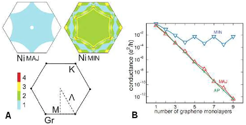
Fig. 2.3.2: (a) Fermi surface projections for fcc Ni (111) majority and minority spins and graphene/graphite.
(b) Conductance for Ni/Grn/Ni stack as a function of the number of graphene monolayers for minority
spin in P(blue), majority spin in P (red) and both carriers in AP (green) [13].
However, there are more reasons that warrant spintronic research of graphene [14], [15]. Currently, very high TMR values have been observed in epitaxial stacks of Fe/MgO/Fe (180% at RT) [13]. Epitaxial growth is difficult to achieve, partly because there is a relatively large lattice mismatch of 3.8 % between Fe and MgO. Therefore alloys of FeCoB instead of Fe, are sometimes used, which, after a post annealing treatment, form a more or less epitaxial structure with MgO [16]. However, TMR values (and spin injection) in these systems remain very sensitive to the exact interface structure and there is a significant gap between observed and predicted TMR values.
Recently, Kelly et al. proposed a CPP MTJ of Ni/graphene/Ni or Co/graphene/Co that would be less sensitive to interface structure and would function in a manner akin to the earlier mentioned spin-filter [13]. The functioning principle of these MTJs can be seen in figure 2.3.2a. At the Fermi energy, graphene only has states at the K-point (or Dirac point). Ni majority electrons do not have available states at or close to the K-point, but Ni minority electrons do. As a consequence, in case of
conservation of crystal momentum, majority electrons can only tunnel through the graphene separation layer, while minority electrons can both tunnel and use the graphene channel at the K-state. The rate of tunneling decreases exponentially with the number of graphene monolayers, while the transport of minority electrons through the channel at the K-state remains relatively constant, as can be seen in figure 2.3.2b. For conservation of momentum, an epitaxial interface between
graphene and the FM is needed. The lattice mismatch between Ni/graphene and Co/graphene is only 1.3% and 1.9%, respectively. To prevent hybridization between the FM and graphene, a small
2 Physical background Page 16 A CNT is basically a sheet of graphene, which is folded into a cylindrical shape of a few nanometers in diameter; the electronic structure depending on the exact folding (metallic or semiconductor) [4]. When returning again to graph 2.3.1, it can be seen that, with regard to the spin relaxation length, the performance of a CNT is almost on par with GaAs. However graphene, with a spin relaxation length between 1.5 and 2 μm [1], [19], lags orders of magnitude behind. It begs the question why there is such a big gap between graphene and a CNT, though they share high mobilities and have the same atomic building blocks.
Aside from the fact that the structure, and thus the electronic behavior, is different, there are also additional explanations possible. One of these was already hinted at: the measurement settings are not comparable. The CNT measurement involves a single molecule [20], while the graphene
measurement comes from a large flake. Another cause could originate from a difference in history. Graphene was discovered in 2004 [21]; while carbon nanotubes have been known at least since 1991. Graphene was first made by mechanical exfoliation, though since then, many other fabrication techniques have reported [22], [23]. The graphene in figure 2.3.1, was made by exfoliation and displays a mobility of 2000 cm2 (Vs)-1 [1]. Mechanical exfoliation is known to create more defects than some alternatives, which can serve as (spin) scattering sites. Tombros et al. concede in their paper, that by improving their fabrication procedures, both τ and μ, and thus lS, could be increased.
2 Physical background Page 17
2.4
Spin injection and detection
Detection of injected spins is not a trivial matter. There are number of different techniques, but detection by electronic measurements is commonly used and is applicable for most materials. A simple two terminal measurement of magnetoresistance (MR) would seem the most logical approach, but does not irrefutably prove spin injection. So called spurious effects give rise to MR effects, but are in fact not related to the earlier discussed GMR and TMR effects [4]. Among the many spurious effects is the earlier mentioned LMR effect. The Lorentz force curves the electron
trajectories and is especially relevant in materials with relatively long mean free paths. The Lorentz magnetoresistance is of the order [4]:
+/ ,- (6)
In which the magnetic length, lB, can also be rewritten as:
, .//0 (7)
Where h is Planck’s constant and e is the elementary charge. Though two terminal measurements provide only circumstantial evidence for spin injection, some three or four terminal measurement schemes do provide direct evidence.
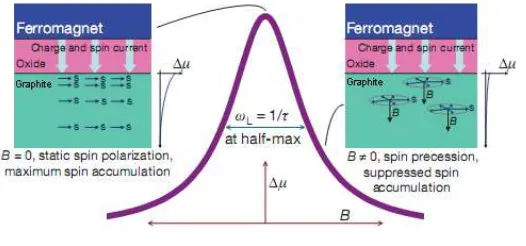
Fig. 2.4.1: Device geometry for a Hanle measurement. The contacts are designated, from left to right, as 1, 2 and 3.
One of these measurement schemes is based on the electrical Hanle effect. A device geometry of a Hanle measurement can be seen in figure 2.4.1. Electrons are injected from the electrode 2 into the graphite and a current runs from the electrode 2 to electrode 3. Excess spin electrons accumulate underneath electrode 2 and start to diffuse in the direction of electrode 1. Since the distance
2 Physical background Page 18
Fig. 2.4.2: Schematic diagram of the DOS of a non magnetic material (a) in equilibrium, and (b) with a finite spin accumulation [24].
In a material with a finite (injected) spin excess density both spin subbands do not have an equal occupation any more (figure 2.4.2b), but there is an imbalance. One of the spin subbands has gained μ↑ energy with respect to the Fermi level, while the other has lost μ↓. This electrochemical potential is defined as12 1 3 45, where μ is the chemical potential, q the charge of a charge carrier and V the voltage. The spin accumulation is defined as61 17 1, where 1 is the electrochemical potential for each respective spin. There is a difference in spin accumulation between contact 1 and 2, which translates into a voltage difference between the contacts via [10]:
65 8 Δµ 2< (8)
In which TSP is the tunnel spin polarization of the ferromagnet-insulator interface.
Fig. 2.4.3: Schematic illustration of a Hanle curve [10].
Applying a magnetic field perpendicular to carrier spins causes precession of the spins, which, via the (electrical) Hanle effect, reduces the spin accumulation underneath contact 2. This is picked up by the voltage probe, resulting in a curve similar to the one shown in figure 2.4.3. The spin precession frequency, ωL depends on the magnetic field, B, via [10]:
=>?@ħA, (9)
2 Physical background Page 19
Fig. 2.4.4: Device geometry for a non-local measurement. The contacts are designated, from left to right, as 1, 2, 3 and 4. In contrast, with the non-local measurement scheme the spin relaxation length can be directly measured. A device geometry of this measurement scheme can be seen in figure 2.4.4. Polarized electrons are injected from electrode 3 into graphite, accumulate and start diffusing towards electrode 2. Like in the Hanle geometry, external electrode 1 measures the potential difference with electrode 2. However, because the distance between 3 and 2 is close to the spin relaxation length, a finite spin accumulation develops at electrode 2. This gives rise to a voltage between contacts 2 and 1 in a similar manner as for the Hanle geometry. However, electrode 2 is also a
ferromagnet-insulator stack and therefore responds differently to the different species. By sweeping the magnetic field parallel to the easy axes of the electrodes an AP and P configuration between electrode 2 and 3 can be achieved. The difference in non-local resistance between the two configurations is given by [25]:
DEDEFG H
%
IJexp 7 O < P (10)
3 Device fabrication Page 20
Chapter 3: Device fabrication
This chapter describes the main activities of this work. A lot of effort was put in the development of fabrication procedures to make a working spintronic device on top of a HOPG substrate. Several techniques were used and a large number of samples were fabricated, which resulted in a number of partially working devices. This chapter is aiming to provide an insight into the device fabrication work that was performed and what kind of (resolved and unresolved) problems were encountered.
Electrical measurements and other kinds of results are treated in the next chapter.
In this project the main three approaches in obtaining spin transport devices were optical lithography and e-beam lithography for fabricating lateral devices and shadow mask deposition for
manufacturing vertical devices. Due to our choice for HOPG and its properties, we encountered a lot of problems that had no counterpart with regular silicon-substrates. The main problems with the structural fabrication were related to the patterning of resist layers on the substrate and the lift-off of deposited materials, so a large section of this chapter is devoted to those two problems.
3.1
Device lay-outs
In developing the fabrication process, several considerations had to be taken into account. Chief point among these considerations was the suspicion that the spin lifetimes in graphene/graphite mentioned in earlier publications, were being significantly influenced by the close proximity of an interface with non-graphite materials. In order to negate this suspected influence, only substrates with a thick graphite layer could be used. Since it is difficult to create a high-quality graphite layer of sufficient thickness on top of a substrate with existing fabrication methods, the choice was made to start with a substrate consisting entirely out of graphite.
3 Device fabrication Page 21 Lateral devices
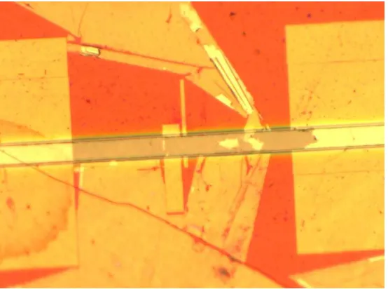
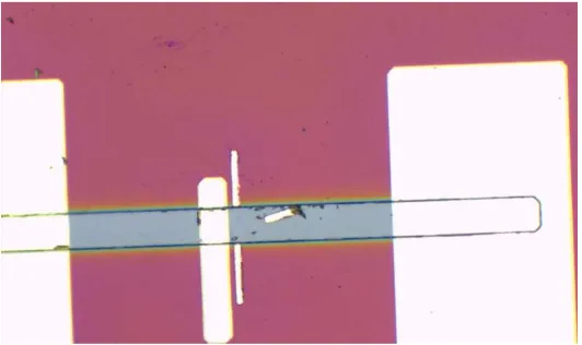
A schematic drawing of the lateral device lay-out can be seen in figure 3.1.1. The device design is based on a similar device that has been previously used in the NE-group to measure electrically created spin polarization in silicon [10]. It is designed to be used for both Hanle and non-local measurements (chapter 2.4), which requires at least four contacts to cancel spurious effects. There are two closely-spaced, narrow ferromagnetic contacts, which need to have different magnetic coercivities in order to perform non-local voltage measurements; something that is achieved by having different contact widths, resulting in different magnetic shape anisotropy. These two smaller contacts also need to be very close to each other, since otherwise spin signals would be difficult to measure due to the spin relaxation. The distances from the two big contacts to the smaller contacts are required to be far larger than the spin diffusion length, since they serve as reference/source contacts; their magnetic properties are not relevant.
Fig. 3.1.1: Schematic drawing of a lateral device. Underlying is the graphite substrate (grey), which is partially isolated by the SiO2 layer (purple). The magnetic contacts consist out of the Al2O3 tunnel barrier and the
ferromagnetic cobalt (together green), which is protected by the capping layer (yellow). The contacts are connected to a measurement apparatus via individual contact pads, which are not shown here.
The basic process flow for a lateral device can be seen in figure 3.1.2. First the graphite substrate is peeled with Scotch tape and put for a short while in an ultrasonication bath in order to make its surface flat and mechanically stable. The next step is to define a channel of 68 x 400 μm on the graphite using photolithography. On top of the developed photoresist a SiO2 layer is deposited. The photoresist is subsequently removed in a lift-off operation with acetone, leaving a channel of uncovered graphite in the SiO2. The SiO2 layer serves as an insulation layer for the later
3 Device fabrication Page 22
Fig. 3.1.2: Schematic diagram of the process flow for a lateral device in which graphite is colored grey, the tunnel barrier and ferromagnetic material green and the capping layers yellow. (a) HOPG substrate after peeling. (b) A SiO2 insulation layer is deposited with a channel of uncovered graphite remaining. (c)
Ferromagnetic contacts are created. (d) Creation of contact pads. (e) The contact pads are connected to a sample holder via wire bonding with silver paste.
In a similar lift-off operation the ferromagnetic contacts are created. Instead of one material, this consists of a stack. The material at the bottom (Al2O3) of the stack is directly in contact with the graphite and serves as a tunnel barrier. Tunnel barriers are used because of the conductivity mismatch problem (graphite-ferromagnet) and to increase the spin accumulation in the graphite. Since the graphite in the channels is not covered, plasma oxidation can not be used and so a 1-2 nm layer of Al2O3 is deposited directly unto the graphite. In the middle of the stack there is the
ferromagnetic material, cobalt, which provides the polarized electrons for injection. On top of this there is a capping layer, which prevents the oxidation of cobalt. For this capping layer different materials were used (Au and Al) and sometimes a combination of the two, in order to combat certain problems in the fabrication process (further discussed below).
The last lithography step is to define the contact pads (figure 3.1.2d). These contact pads connect the small, fragile ferromagnetic contacts to a larger contact, on which a wire can be bonded. The
3 Device fabrication Page 23 Vertical devices
The vertical devices were developed as a response to the problems with the lateral devices. Lift-off and the resolution of photolithography were problematic, which could be circumvented with the vertical geometry. However vertical devices were, because of their geometry, not suitable for non-local measurements, thus only two point and quasi-Hanle measurements were possible. When some of the problems with the lateral devices were solved, attempts with vertical devices were quickly abandoned due to the limitations in possible measurement schemes and the perceived persistent leakage of the tunnel barriers. A schematic drawing of a vertical device can be seen in figure 3.1.3. In the vertical geometry the contacts are defined by shadow mask deposition, which has a poor
resolution. The contacts created are around an order of magnitude larger than their lateral counterparts (2.3x1 mm).
Fig. 3.1.3: Schematic drawing of a vertical device. There is a thin graphite layer in the middle (grey). On both sides of the graphite there is an Al2O3 tunnel barrier (blue). The green, ferromagnetic layer consists in the
lower case out of cobalt; in the upper case out of permalloy. On both sides there is an Al capping layer (yellow). The bottom side is attached to a Si substrate with double sided conducting carbon tape.
The fabrication of vertical devices starts again with a flattened graphite substrate and can be seen in figure 3.1.4. On top of the graphite an Al2O3 tunnel barrier (1 nm) is deposited, followed by a
ferromagnetic Co layer (50 nm) and an Au capping layer (3 nm). Subsequently double sided, conducting tape is applied to the deposition side of the graphite sample and all three deposited layers and some graphite layers are peeled off the graphite sample. The unused side of the double sided tape is attached to a Si substrate and once again inserted into the deposition chamber. On the backside of the peeled-off graphite an even (unpatterned) layer of Al2O3 (1 nm) is deposited as a tunnel barrier. After this a layer of the ferromagnetic Permalloy (50 nm) is deposited through a shadow mask unto the tunnel barrier, thus defining the contacts. On top of the permalloy an Al capping layer (3 nm) is deposited. After that the contacts are connected by manual wire bonding.
3 Device fabrication Page 24
3.2
Substrate preparation
Before discussing the actual fabrication process details, we would first like to elaborate on the properties of the bare graphite substrates themselves. Graphite is a natural polymorph of carbon and is known to be atomically flat on a small scale. The highest quality graphite substrates are single-crystals, but these substrates are expensive and small, which makes them unsuitable for use in a normal lithography process. Instead of these single crystals we use highly oriented pyrolytic graphite (HOPG), which should suffice for our purposes, since our devices have features in the micrometer regime.
A limited number of substrates were bought from the manufacturer SPI [26]; some of which had the dimensions 10 x 10 x 1mm. Also some more 20 x 20 x 1 mm were bought, which could be cut into 10 x 10 x 1 mm pieces. However graphite cannot be easily cut clean through. Using a diamond saw causes a graphite substrate to uncontrollably split into several pieces. A sharp knife on the other hand doesn’t cut easily through graphite, but instead pushes and grinds away some of the materials. This leads to upstanding ridges at the back of the sides that were cut, which later makes it difficult to use a photo mask.
There are several ways to produce graphite, but substrates of such sizes are usually made by
decomposition of for example ethylene unto a surface, though other molecules like ethane, propane and cyclohexane also work [27]. At a local (atomic) level these HOPG-substrates are indeed almost flat, but on a microscopic level they are not. The different HOPG-substrates have different surface structures, which can be seen in figure 3.2.1. The difference in surface structure also affects
fabrication results. The lift-off of the samples in figure 3.2.1a and 3.2.1b for example went flawlessly, while the exact same fabrication procedure performed on the sample shown in figure 3.2.1c,
[image:24.595.76.526.460.593.2]removed all ferromagnetic material from the graphite (but not from the SiO2).
Fig. 3.2.1: Optical microscope images of a small selection of different surface morphologies. Note that these images do no show the graphite directly, but use the SiO2 layer for added contrast. (a) A very flat surface
with a peeling line defect. (b) Slightly sloping surface with major defects locally. (c) Very hilly surface.
3 Device fabrication Page 25 breaks along the peeling direction, leading to trenches like the one seen in figure 3.2.1a. The peeling procedure can also be used to remove deposited layers, thus allowing HOPG substrates to be reused, but each time shrinking in thickness. After finishing the peeling, the HOPG substrates are placed for a short while in an ultrasonic bath in order to remove loose patches of graphite. These loose patches might otherwise unpredictably disconnect from the surface during later fabrication steps, which would result in the loss of surface structures.
Overall it can be said that the surface defects, the roughness, different surface morphologies and constantly shrinking thicknesses of the substrates upon repeated peeling steps, result in a highly inhomogeneous surface and unpredictable results with later fabrication steps.
3.3
Contact patterning
In this section, the three ways that were used in this work for patterning structures on the graphite surface will be discussed. Note that with both lithography methods a similar structure (lateral device) was made, whereas the shadow mask technique was used to create a different structure (vertical device). Details of the fabrication processes can be found in appendix A and examples of some of the used masks can be found in appendix B.
Photolithography
Optical lithography was the starting approach for patterning the substrate. Photolithography was used because the tools for optical lithography were freely available in the cleanroom. Also, in contrast with shadow mask deposition, UV-photolithography can provide feature sizes down to 1 μm, which is a requirement for non-local devices.
After removing the substrate from the ultrasonication bath, a photoresist layer is spun on top of it. The photoresist TI-35ES [28] was chosen for this purpose, since it was the only resist suitable for a lift-off operation that is readily available in the MESA+ cleanroom. Two features make it attractive as a lift-off resist. First of all it has an undercut, which, during the later deposition, enhances the natural shadow-effect. Second it is a relatively thick resist (3.5 μm), so lifting-off a relatively thick layer is a possibility. In figure 3.3.1, a schematic diagram of the general lithography process of TI-35 is depicted. The precise recipe can be found in appendix A, which was adapted (with minor changes) from a recipe used by an earlier master thesis in the NE-group [29].
3 Device fabrication Page 26 After having spun the photoresist, the photoresist is baked for a short while in order to harden out. Next is the first exposure, during which the small graphite substrate is placed in a wafer-sized sample holder. The substrate is fixed in a cavity of this sample holder by layers of adhesive tape at the bottom (figure 3.3.2). These adhesives tape layers also serve to bring the surface of the substrate at approximately the same level as the sample holder’s. A photo mask is placed very tightly on top of the photoresist and the photoresist is illuminated by UV-light through the openings in the photo mask for a brief period of time, thus defining the pattern. Ti-35 is an image reversal resist, meaning that the parts of the photoresist that were exposed to the light during the first exposure will remain after development. The first exposure dose (together with the later development time) determines the eventual undercut of the photoresist. A lower exposure dose typically yields a stronger undercut.
Fig. 3.3.2: Schematic drawings of (a) sample holder, (b) sample holder with respect to the position of the photo mask and the substrate.
After a brief waiting period in order to allow for the out gassing of N2 out of the photoresist, the resist is again baked. This reversal bake serves to crosslink the polymers in the previously exposed areas of the photoresist, making these parts resistant to both the developer and exposure to light. Afterwards the sample is again, this time without a photo mask, illuminated during a flood exposure. This flood exposure step serves to make the previously unexposed areas soluble to the developer. After the flood exposure, the photoresist is developed using OPD 4262 (standard developer), thus revealing the negative, reversed image of the photo mask.
One of the problems in this master thesis was to obtain a high enough resolution to define a pattern on graphite. With the photolithography facilities in the cleanroom feature sizes of 1-2 μm can be achieved at best. However the distance between the two smaller contacts in the lateral devices ought to be 2 μm or less, so obtaining the maximum resolution was absolutely paramount. The most critical step in the fabrication process is the first exposure, and more specifically the approach and placement of the photo mask. Failure to limit the distance between a photo mask and the underlying sample to a uniform and absolute minimum, leads to a noticeable reduction in resolution due to diffraction effects.
3 Device fabrication Page 27 Fig. 3.3.3: Optical microscope images of two common photolithography problems. (a) Holes in the photoresist
likely caused by depositing graphite flakes on the photo mask during aligning. (b) Curved photo resist in between the two future smaller contacts probably due to excess undercut. Excess undercut might also be the cause for some of the observed resolution problems. Some thin, undercut lines of photoresist could break, resulting into two smaller contacts without a separation wall.
Eventually however a few “tricks” and adaptations in fabrication process were made by which photolithography became more reliable, though at times still unpredictable. The photo mask was modified to have a variety of contact distances ranging between 2-5 μm, thus always yielding some usable devices. Furthermore, before starting the fabrication process, each sample was measured at three different points in order to assess its thickness. Depending on the measured thickness a number of layers of tape (60-80 μm each) were placed underneath the sample in the sample holder. During fabrication of a sample three photolithography steps had to be done, while only the second (the ferromagnetic contact) was critical in resolution. The first lithography step (defining the channels) thus often served as a test run for the number of layers. One of the final modifications to the fabrication process was to increase the first exposure time from 20 to 24 seconds, to increase resolution and to prevent problems suspected to be caused by excess undercut (see figure 3.3.3b). These measures led to contact distances of 3 μm being quite regularly made, some 2.5 μm, and 2 μm being rare.
E-beam lithography
E-beam lithography was briefly considered as an alternative to photolithography. The two main reasons being its superior resolution (120 nm on graphite) and because no photo mask is required. However e-beam lithography is a writing technique and thus the time required to write a pattern is quite long. Therefore only the second lithography step (the ferromagnetic contacts) was done by e-beam writing, since the other two could be done quite easily with photolithography.
For e-beam lithography PMMA was used, which is a positive photoresist, meaning that the exposed areas become soluble. This photoresist is spun on the sample and then baked. Subsequently the sample is put in a vacuum chamber and locally exposed to a stream of electrons. The exposure of areas is done in square blocks of 100 μm, which are “stitched” together. The fact that e-beam writing uses a stream of electrons both to write and to inspect a pattern requires that the layers of resist are typically thin (in our case 100 nm). Afterwards the PMMA layer is developed with MIBK as a
3 Device fabrication Page 28
Fig. 3.3.4: Effects of acetone soak and 90 seconds of ultrasonication on the contacts. Also note the stitches in the two big contacts.
The results of the e-beam writing on graphite were good, though there was a problem with the stitching in the two big contacts, which could possibly be remedied by later depositing the contact pads over the gaps. The achieved resolution easily exceeded that of photolithography: patterns of contact distances of 1 μm were made. However the problems with the e-beam approach were encountered when doing the lift-off, since PMMA is not a photoresist particularly suited for lift-off. It does not have an undercut and because of its thickness (100 nm) only thin layers can be deposited. A ferromagnetic stack of in total only 12 nm thick was deposited (Al2O3, Co, Au 1, 10 and 1 nm
respectively thick). Several methods of removing this very thin layer were tried, but none of these could remove the layer without causing major damage. The lift-off problems were probably caused by depositing under an oblique angle, but no additional attempts were made to resolve this. E-beam lithography was thus discontinued because of this lift-off problem, but also because it was perceived that layers of about 10-30 nm would not be a very robust building block.
Shadow mask deposition
Shadow mask deposition was used to pattern the alternative vertical spin devices of graphite, since it proved to be difficult to create the originally intended lateral spin devices by the two previous methods. The resolution of this technique is mainly determined by the way in which the shadow mask is fabricated. In our case a laser cut an array of rectangles (2.3 x 1.5 mm) out of a thin steel plate; a technique that has a possible minimum feature size of several hundreds of micrometers. The exact shadow mask can be seen in appendix B.
3 Device fabrication Page 29 Peeling off the ferromagnetic stack and some graphite layers proved to be the most critical part of this process. Since these peeled off layer is very thin, they are prone to break during the peeling, resulting in some open gaps in the layers. It would be undesirable to have such a gap underneath a contact; minimal contact sizes were therefore preferable to increase the chance of having contacts without such a gap. However during later electrical measurements, problems were encountered, which were thought to be tied to these gaps. For this reason and for the fundamental measurement limitations of the vertical device structure, attempts at shadow mask deposition were halted in favor of lateral devices.
3.4
Deposition and lift-off
The general process flow for a lift-off operation is depicted in figure 3.4.1. After having applied a photoresist layer, it is illuminated and developed. Afterwards a layer is deposited on top of the photoresist. The photoresist TI-35 has an undercut after developing, which aids the lift-off by enhancing the natural shadowing effect of the photoresist layer during deposition. The remaining photoresist is subsequently removed by dissolving it in acetone. Because of the shadow-effect during deposition, there should, in principle, be little or no material connecting the layer of deposited material that was formerly on top of the photoresist and the one that was deposited directly unto the sample. Since this connection is non-existent or very thin, the obsolete deposited layers could in principle be removed easily by applying a modest force through for example ultrasonication, leaving the desired pattern intact.
Fig. 3.4.1: Schematic diagram of lift-off process used for creating a lateral device. (a) Photoresist as applied. (b)
Developed photoresist with undercut. (c) Deposition of material on photoresist. (d) Lift-off of the material, leaving behind the desired structure.
However in the early fabrication runs it was observed that using a modest force did not suffice to separate the obsolete layers from the surface. A remedy for this would have been to apply more force instead, an approach often used with silicon samples, but this was not a viable option in the case of graphite samples. Since graphite is not robust and has low surface adhesion, the graphite substrate itself or some of the more delicate patterned features were often damaged, before the lift-off was totally completed. Therefore, during the earlier fabrication runs an unpredictable trade-lift-off was made between local damage to the sample and the amount of lifted-off area in the hope that a sufficient amount of devices survived on a single sample to be usable.
3 Device fabrication Page 30
Fig. 3.4.2: Schematic drawing of deposition (a) under an oblique angle (b) perpendicular to the substrate.
Depositing under an oblique angle can create on one side of the opening in the photoresist a firm connection to the obsolete layer, while on the other side an enhanced shadow effect is created. This enhanced shadow effect can in principle be seen, when observing from a perpendicular viewpoint.
Fig. 3.4.3: Shadow effects observed when depositing from (a) an oblique angle (b) a more or less perpendicular direction. Shadow effects were indeed observed after the deposition of the ferromagnetic stack as can be seen in figure 3.4.3a, but were not directly observed when depositing the SiO2 and the contact pads. The absence of the shadow can be explained by the difference in deposition conditions. During the deposition of the ferromagnetic stack the sample is fixed with respect to the source, while in the two other cases the sample is rotating. Using a different sample position for depositing the ferromagnetic stack removed the shadow effect as can be seen in figure 3.4.3b, which resolved most of its lift-off problems. The lift-off problems for the contact pads were resolved by using different materials, which allowed it to be deposited in the same apparatus as the ferromagnetic stack. This could not be done for the SiO2 deposition, but its lift-off was found to go far easier as an unintended consequence of modifications of its sputtering equipment during maintenance.
The remainder of this section is divided into three subsections in which the details of the deposition and lift-off of each material stack will be discussed. Since each of these materials stack had different challenges and related phenomena, it is fruitful to discuss them separately.
Silicon Dioxide
3 Device fabrication Page 31 SiO2 is deposited using a homemade sputtering system (TCoater). Several samples are put in a wafer-sized holder, which is placed in the TCoater’s chamber at 44 mm from the SiO2 target. After having pumped down the chamber, it is subsequently filled with Argon gas up to a pressure of 0.004 Torr. A plasma can be generated by applying a magnetic and electric field, which deposits the SiO2 from the target unto the samples. In this case an RF instead of a DC field has to be used, since SiO2 is insulating and would thus prevent continued sputtering by charging. A total layer of roughly 500 nm was deposited at an approximate rate of 8 nm/min. The height of this layer rises abruptly with 175nm at the edges; afterwards rising steadily to the total of 500 nm.
One of the peculiar things was that some samples were dotted with discolorations, as can be seen in figure 3.4.4. These discolorations were not observed on bare graphite, but only on the places where a layer was already deposited. These dots were in most cases only observed on places with an underlying SiO2 layer.
Fig. 3.4.4: SiO2 surface dotted with discolorations. (a) Wide view, showing the almost uniform distribution of the
dots. (b) Close up, showing the different sizes of dots.
The dots were also briefly studied with an AFM. As can be seen in figure 3.4.5, the dots are actually mounds. Only a small number of these mounds have been studied, but their heights seem to be ranging roughly between 150 and 300 nm.
Fig. 3.4.5: AFM tapping mode images of the observed discolorations.
The cause for the formation of these types of mounds was not elucidated, but excessive heating seemed to increase their number. It was however suspected that their formation could be originating from absorbed droplets of fluid within the HOPG substrate. Thermal expansion of this fluid,
3 Device fabrication Page 32 As was discussed in the previous paragraph a proper and gentle lift-off was essential during
[image:32.595.168.431.128.324.2]fabrication, since a problematic lift-off would render a lot of devices on a sample unusable. An example of damage sustained during one of these lift-off operations can be seen in figure 3.4.6.
Fig. 3.4.6: Damage sustained to the SiO2 layer during ultrasonication.
In figure 3.4.6 two types of damaged areas can be distinguished. On the one hand there are the grey areas. Here, the deposited layers have been totally removed and the graphite is laid bare. On the other hand there areas the surrounding the previously mentioned category, that have roughly the same height as the undamaged areas, but do have a distinct color compared to the undamaged areas. Inspection with AFM indicated that these areas consist out of SiO2 that is still partially attached to the undamaged areas and also slightly tilted.
The earlier mentioned mounds could also be related to this ultrasonication damage. One sample without any observable dots was placed in an ultrasonic bath for several minutes without sustaining major damage, while other samples already displayed damage after ultrasonication for less than a minute. It can be reasoned that these mounds function as weak spots, being more prone to break during ultrasonication, because of them missing a direct mechanical contact to the underlying substrate.
The problem of the lift-off of the SiO2 layer was eventually largely solved, probably partly as an accidental consequence of maintenance of the TCoater. Additionally the adhesion between the graphite and the SiO2 was significantly better than in the case of the other materials, making it a less troublesome lift-off than in the case of those materials.
Ferromagnetic stack
3 Device fabrication Page 33 deposit unto the surface. A low pressure is maintained during deposition by a liquid nitrogen cooled baffle. The deposition rate can be very accurately monitored by a vibrating quartz-crystal, while the deposition itself is stopped and started by opening/closing a shutter. In principle the DCA also has the ability to do shadow-mask deposition, which was used in the case of the vertical spin devices.
Au (50 nm) Au (100 nm) Au (3 nm)
Cr (30 nm) Al (130 nm) Al (100 nm)
Au (50 nm) Au (3 nm) Au (50 nm) Au (3 nm)
Al (50 nm) Al (3nm)
Co (50 nm) Co (100 nm)
Al2O3 (1 nm) Al2O3 (2 nm) (Rotating deposition)
Fig. 3.4.7: Composition and thicknesses used for the ferromagnetic stacks and contact pads of different samples.
The first of these layers to be deposited is the tunnel barrier. A layer of 1-2 nm of Al2O3 is used for this purpose. Al2O3 is known to have a high degree of uniformity and flatness, making it a suitable material for research. In order to create an Al2O3 tunnel barrier the usual method is to deposit Al and to subsequently plasma oxidize it. However, this is not suitable when using a HOPG substrate, so instead Al2O3 is deposited directly. To remove any remaining oxygen vacancies in the Al2O3, the sample is naturally oxidized in pure oxygen (100 mTorr) in the adjacent loadlock of the DCA. These oxygen vacancies could otherwise create defects, which would prevent the tunnel barrier from properly functioning. The next layer to be deposited is the ferromagnetic material; in our case cobalt was used. To prevent cobalt from oxidizing, an additional capping layer is deposited directly unto it. For this capping layer different materials were used: gold, aluminum or a combination thereof. Throughout the project different compositions and thicknesses of these stacks were used in order to improve the yield/performance of the fabricated devices. A schematic of the different thicknesses and compositions can be seen in figure 3.4.7.
The lift-off procedure used for the ferromagnetic stack was similar to the one described for SiO2 (see above). The developed photoresist TI-35 underneath the deposited ferromagnetic stack was
[image:33.595.98.529.141.215.2]3 Device fabrication Page 34
Fig. 3.4.8: Breaking of a small ferromagnetic contact after ultrasonication. The broken-off section is still lying in the channel. A different problem was again related to depositing under an angle. As can be seen in figure 3.4.9, for some samples a shadow image of the ferromagnetic contacts can be seen. This was a major problem, because a part of the shadow contact was not in contact with the tunnel barrier, but directly with underlying graphite. The cause for this lay in the fact that the ferromagnetic stack was deposited with two different e-beam deposition guns, with each having a different position (and angle) with respect to the sample during deposition.
Fig. 3.4.9: Optical microscope of a deposition shadow of the ferromagnetic stack.
The problem could not be resolved by a different choice of materials, since Al2O3 was in Gun 1, and all the ferromagnetic materials were situated in electron Gun 2. Swapping materials between guns is non-trivial, and should be considered only as a last resort, since it will affect all deposition processes in which the DCA is used. One of the ways in which we tried to resolve this was depositing Al2O3 from four different angles (0°, 90°, 180° and 270°), thus depositing Al2O3 in the undercut of the
photoresist. This method presumably resulted in a tunnelbarrier of 0.5 nm thick at the edges and 2 nm in the middle, but at least in this way it was ensured that everywhere underneath the cobalt a tunnelbarrier was present. Also Al was subsequently used as a capping layer, since it was located in the same e-gun as the cobalt.
[image:34.595.192.406.364.542.2]3 Device fabrication Page 35 deposition positions and subsequently assuming that the ones with a proper lift-off had, for all practical purposes, a more or less perpendicular angle with respect to the trenches. Since at that time the thicknesses of Al2O3 and Au were negligible to Co (1, 3 and 50 nm, respectively), the
[image:35.595.81.519.190.344.2]problems derived from use of two different guns were realized only late in the stage of my project. A fellow master student, Koert Vergeer, determined later the proper deposition positions for both guns. It turned out that I would only have had to turn the sample 180° around for the different guns in order to solve this issue.
Fig. 3.4.10: (a) SEM image ofsmall ferromagnetic contacts with a big deposition shadow. (b) Optical image of contacts presumably with partially oxidized cobalt at the exposed shadow.
The shadowing caused some additional problems. In some devices the lateral displacement by the shadowing effect was so big, that the gap between the two smaller contacts could be bridged. This can be seen in figure 3.4.10a. In addition in the same picture a shadow layer of the right contact is seen to hang partially loose. Additional measurements with the AFM indicated that this was not a rare occurrence. These loose and potentially movable patches could possibly be one of the causes for irreproducible electrical measurements (see chapter 4.2). Additionally, some shadow contacts degraded over time, as can be visually seen in figure 3.4.10b. This is probably the cobalt layer partially oxidizing. This was resolved by using aluminum as a capping layer, since both Co and Al come from the same e-guns.
[image:35.595.78.518.547.719.2]3 Device fabrication Page 36 In the later contacts yet again a problem surfaced. In order for tunneling to become the dominant transport mechanism, it is necessary to cool down the sample to very low temperatures. While measuring these devices, sometimes, at certain temperatures, signals abruptly decayed into noise and no signal could be observed anymore at this temperature. Upon raising the temperature again, on certain occasions the signals returned at a certain temperature (< 230 K), and an IV-curve could once again be measured. Afterwards the sample was inspected underneath an optical microscope and using the SEM, as can be seen in figure 3.4.11. The discolorations were reminiscent of the dots in SiO2, which were earlier observed (see figure 3.4.4). The SEM image shows a surface, which,
[image:36.595.126.474.251.367.2]especially in the graphite channel, is highly inhomogeneous and wrinkled. Furthermore, in AFM tapping-mode studies, a height and phase difference was observed between the distorted and un-distorted areas.
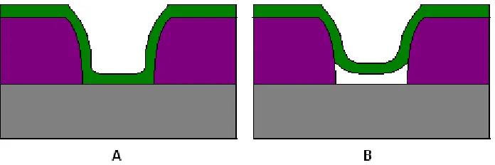
Fig. 3.4.12: Schematic drawing of a possible scenario for release of thermal strain in the lateral device. (a) At room temperature the ferromagnetic stack (green) is firmly attached to the SiO2 (purple) and graphite (grey).
(b) At low temperatures the ferromagnetic layer ruptures from the graphite substrate, due to the low adhesion to and difference in thermal expansion with the graphite.
A possible cause for the damage sustained during the cooling, might come from using different materials, with different thermal expansion coefficients, for the ferromagnetic stack. Aluminum has the highest thermal expansion coefficient (22 K-1) of the four stack materials, while graphite has a lateral coefficient of only around 8 K-1 [31]. It is possible to consider a scenario as sketched in figure 3.4.12, in which the ferromagnetic contact contracts, resulting in losing contact with the conducting graphite. Since it is very difficult to look underneath the ferromagnetic stack, this idea could not be confirmed, but the earlier mentioned observations make it very probable that something mechanical happens during cooling. Trying to overcome this problem we reduced the thickness of the Al layer from 50 to 3 nm and increased the Co layer thickness to 100 nm. Since cobalt has a thermal expansion coefficient of about 12 K-1 [31], it was thought this could resolve the problem. However, during lift-off of the ferromagnetic stack most contacts were destroyed in the channel, while