Modeling and simulation of magnetic components in electric circuits
290
0
0
Full text
(2) UNIVERSITY OF SOUTHAMPTON. MODELING AND SIMULATION OF MAGNETIC COMPONENTS IN ELECTRIC CIRCUITS. PETER REID WILSON. SUBMITTED FOR THE DEGREE OF PHD. DEPARTMENT OF ELECTRONICS AND COMPUTER SCIENCE NOVEMBER 2001. i.
(3) UNIVERSITY OF SOUTHAMPTON. ABSTRACT FACULTY OF ENGINEERING DEPARTMENT OF ELECTRONICS AND COMPUTER SCIENCE Doctor of Philosophy MODELING AND SIMULATION OF MAGNETIC COMPONENTS IN ELECTRIC CIRCUITS by Peter Reid Wilson. This thesis demonstrates how by using a variety of model constructions and parameter extraction techniques, a range of magnetic component models can be developed for a wide range of application areas, with different levels of accuracy appropriate for the simulation required. Novel parameter extraction and model optimization methods are developed, including the innovative use of Genetic Algorithms and Metrics, to ensure the accuracy of the material models used. Multiple domain modeling, including the magnetic, thermal and magnetic aspects are applied in integrated simulations to ensure correct and complete dynamic behaviour under a range of environmental conditions. Improvements to the original Jiles-Atherton theory to more accurately model loop closure and dynamic thermal behaviour are proposed, developed and tested against measured results. Magnetic Component modeling techniques are reviewed and applied in practical examples to evaluate the effectiveness of lumped models, 1D and 2D Finite Element Analysis models and coupling Finite Element Analysis with Circuit Simulation. An original approach, linking SPICE with a Finite Element Analysis solver is presented and evaluated. Practical test cases illustrate the effectiveness of the models used in a variety of contexts. A Passive Fault Current Limiter (FCL) was investigated using a saturable inductor with a magnet offset, and the comparison between measured and simulated results allows accurate prediction of the behaviour of the device. A series of broadband hybrid transformers for ADSL were built, tested, modeled and simulated. Results show clearly how the Total Harmonic Distortion (THD), Inter Modulation Distortion (IMD) and Insertion Loss (IL) can be accurately predicted using simulation. A new implementation of ADSL transformers using a planar magnetic structure is presented, with results presented that compare favourably with current wire wound techniques. The inclusion of transformer models in complete ADSL hybrid simulations demonstrate the effectiveness of the models in the context of a complete electrical system in predicting the overall circuit performance.. ii.
(4) List of Contents Abstract............................................................................................................................................ ii List of Contents .............................................................................................................................. iii List of Figures................................................................................................................................. ix List of Tables ................................................................................................................................ xvi Acknowledgements...................................................................................................................... xvii Declaration.................................................................................................................................. xviii List of Abbreviations ................................................................................................................... xix 1. Introduction ............................................................................................................................ 1 1.1 Project Motivation and Goals .......................................................................................... 1 1.2 Definition of systems to be simulated.............................................................................. 2 1.2.1 Identification of Target Application Areas.................................................................. 2 1.2.2 Key Issues to be addressed in Application Simulations .............................................. 3 1.3 Application specific modeling and simulation techniques .............................................. 4 1.3.1 Techniques Required for SMPS component modeling ................................................ 4 1.3.2 Techniques required for Fault Current Limiting......................................................... 5 1.3.3 Techniques required for Broadband Hybrid Transformers ........................................ 6 1.4 Project Scope ................................................................................................................... 6 1.4.1 Introduction................................................................................................................. 6 1.4.2 Structure of the Project ............................................................................................... 7 1.4.3 Specific Project Hypotheses ........................................................................................ 8 1.5 Thesis Structure ............................................................................................................... 9 1.5.1 Chapter 1 : Introduction.............................................................................................. 9 1.5.2 Chapter 2 : Review of Modeling and Simulation Theory ............................................ 9 1.5.3 Chapter 3 : Review of Magnetic Material Modeling................................................... 9 1.5.4 Chapter 4 : Implementation and Characterization of Magnetic Material Models ... 10 1.5.5 Chapter 5 : Modeling Windings ................................................................................ 10 1.5.6 Chapter 6 : Modeling Magnetic Components ........................................................... 10 1.5.7 Chapter 7 : Modeling a Simple transformer ............................................................. 10 1.5.8 Chapter 8 : Coupled SPICE-Finite Element Analysis Simulation ............................ 10 1.5.9 Chapter 9 : Dynamic Electric-Magnetic-Thermal Modeling.................................... 11 1.5.10 Chapter 10 : Modeling a Passive Fault Current Limiter...................................... 11 1.5.11 Chapter 11 : Modeling Broadband Hybrid Transformers .................................... 11 1.5.12 Chapter 12 : Discussion and Conclusions ............................................................ 11. 2. Review of Modeling and Simulation Theory...................................................................... 13 2.1 Modeling Theory ........................................................................................................... 13 2.1.1 Introduction to Modeling and Simulation ................................................................. 13 2.1.2 Continuous and Discrete Time Simulation................................................................ 13 2.1.3 Definition of a Model ................................................................................................ 14 2.1.4 Electrical System Modeling....................................................................................... 16 2.1.5 Thermal System Modeling ......................................................................................... 17 2.1.6 Magnetic System Modeling ....................................................................................... 18 2.1.7 Mixed System Modeling – Electromagnetic .............................................................. 19 2.2 Component Modeling Techniques................................................................................. 20 2.2.1 Introduction............................................................................................................... 20 2.2.2 Behavioural Modeling using Hardware Decription Languages ............................... 20 2.2.3 Behavioural Modeling using Macro-Modeling ......................................................... 20 iii.
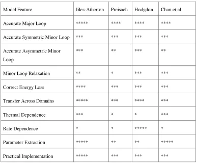
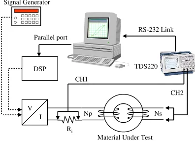
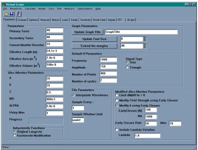
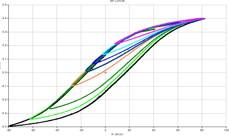
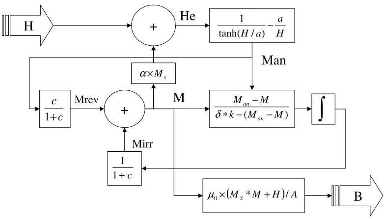
(5) 2.2.4 Structural/Component Level Modeling ..................................................................... 21 2.3 Circuit Simulation Techniques ...................................................................................... 21 2.3.1 Solving linear equations using Gaussian Elimination .............................................. 21 2.3.2 Circuit Elements and Netlists .................................................................................... 23 2.3.3 Solving Non-linear Equations ................................................................................... 23 2.3.4 Integration Methods .................................................................................................. 25 2.3.5 Time Domain Simulation........................................................................................... 27 2.3.6 Small Signal AC Analysis .......................................................................................... 27 2.4 Electro-Magnetic Device Modeling............................................................................... 28 2.4.1 Introduction............................................................................................................... 28 2.4.2 Finite Element Analysis............................................................................................. 28 2.4.3 Tubes and Slices ........................................................................................................ 29 2.4.4 Finite Difference ....................................................................................................... 29 3. Review of Magnetic Material Modeling ............................................................................. 31 3.1 Introduction to Magnetism in Soft Ferrite Materials ..................................................... 31 3.2 Magnetic Material Definitions, Metrics and Model Requirements ............................... 33 3.2.1 Introduction............................................................................................................... 33 3.2.2 Hysteresis Loop Definitions ...................................................................................... 33 3.2.3 Hysteresis Loop Metrics............................................................................................ 35 3.2.4 Energy Considerations .............................................................................................. 37 3.2.5 Relaxation of Minor Loops........................................................................................ 38 3.2.6 First Order Reversal Curves ..................................................................................... 39 3.2.7 Temperature Dependence of Hysteresis Loops ......................................................... 39 3.2.8 Frequency Dependence of Hysteresis Loops and Eddy Currents ............................. 40 3.2.9 Summary of Magnetic Material Model Requirements............................................... 40 3.3 Magnetic Material Models of Hysteresis....................................................................... 40 3.3.1 Introduction............................................................................................................... 40 3.3.2 Rayleigh Loop Model ................................................................................................ 41 3.3.3 Jiles-Atherton Model ................................................................................................. 42 3.3.4 Preisach Model ......................................................................................................... 44 3.3.5 Chan-Vladirimescu Model ........................................................................................ 48 3.3.6 Hodgdon Model......................................................................................................... 49 3.3.7 Comparative Studies of Models................................................................................. 50 3.4 Magnetic Material Model Summary.............................................................................. 51. 4. Implementation and Characterization of Magnetic Material Models............................. 52 4.1 Introduction ................................................................................................................... 52 4.2 Methods of Testing Magnetic Materials........................................................................ 52 4.2.1 Introduction............................................................................................................... 52 4.2.2 DSP Test Configuration ............................................................................................ 53 4.2.3 Magnetic Materials Tested........................................................................................ 55 4.2.4 Calculation of Magnetic Field and Flux Density ...................................................... 55 4.2.5 BH Curve Analysis Software ..................................................................................... 55 4.3 Example Magnetic Material Test Results...................................................................... 56 4.3.1 Introduction............................................................................................................... 56 4.3.2 Philips 3F3 BH Major Loop Measurements ............................................................. 57 4.3.3 First Order Reversal Curves ..................................................................................... 57 4.4 Implementation of Magnetic Material Models .............................................................. 58 4.4.1 Introduction............................................................................................................... 58 4.4.2 Original Jiles-Atherton Model implemented in PSPICE........................................... 58 4.4.3 Inclusion in PSPICE Circuit Simulation Model........................................................ 60 4.4.4 Problem of δK Convergence and Proposed Solution................................................ 61 4.4.5 Modification to Jiles-Atherton model to improve loop closure modeling ................. 63 4.4.6 Comparison of Measured and Simulated Results...................................................... 65 4.4.7 Comparison of original and modified Jiles-Atherton model..................................... 68 4.5 Parameter Extraction and Characterization ................................................................... 69 iv.
(6) 4.5.1 Measurement of Basic BH Curve Metrics ................................................................. 69 4.5.2 Comparison of Metric based and Least Squares Error Functions............................ 72 4.5.3 Implementation of Metric and Parameter Extraction Software ................................ 73 4.6 Optimization of Magnetic Material Models .................................................................. 75 4.6.1 Introduction............................................................................................................... 75 4.6.2 Magnetic Material Model Optimization procedure .................................................. 76 4.6.3 Overview of Optimization Methods........................................................................... 76 4.6.4 Comparison of Optimization Methods....................................................................... 80 4.6.5 Statistical Analysis of Optimization Methods............................................................ 82 4.6.6 Multiple Loop Optimization ...................................................................................... 83 4.7 Dynamic Minor Loop Modeling.................................................................................... 85 4.7.1 Introduction............................................................................................................... 85 4.7.2 Outline of Minor Loop Modeling using Turning Points............................................ 86 4.7.3 Testing the modified Jiles-Atherton model behaviour............................................... 86 4.7.4 Implementation of the volume fraction modification using MAST ............................ 87 4.7.5 Summary of Dynamic Minor Loop Modeling............................................................ 89 4.8 Conclusions ................................................................................................................... 89 5. Modeling Windings and Parasitics ..................................................................................... 91 5.1 Introduction ................................................................................................................... 91 5.2 Introduction to Winding Models ................................................................................... 91 5.3 Leakage Inductance ....................................................................................................... 92 5.3.1 Definition................................................................................................................... 92 5.3.2 Theoretical Methods.................................................................................................. 93 5.3.3 Measurement Methods .............................................................................................. 93 5.3.4 Numerical Methods ................................................................................................... 94 5.3.5 Issues with unusual winding configurations ............................................................. 94 5.3.6 Effect of Core Gaps and Geometry on Leakage Inductance ..................................... 95 5.4 Capacitance.................................................................................................................... 95 5.4.1 Background ............................................................................................................... 95 5.4.2 Theoretical Methods.................................................................................................. 96 5.4.3 Measurement Methods .............................................................................................. 96 5.4.4 Numerical Methods ................................................................................................... 97 5.5 Winding Losses ............................................................................................................. 97 5.5.1 Background ............................................................................................................... 97 5.5.2 Theoretical Methods.................................................................................................. 98 5.5.3 Measurement Methods .............................................................................................. 99 5.5.4 Numerical Methods ................................................................................................... 99 5.6 Proximity Effect .......................................................................................................... 100 5.7 Summary...................................................................................................................... 101. 6. Modeling Magnetic Components ...................................................................................... 102 6.1 Introduction ................................................................................................................. 102 6.2 Electrical vs Mixed Domain Modeling........................................................................ 102 6.2.1 Introduction to Electrical Modeling........................................................................ 102 6.2.2 Mixed Technology Modeling ................................................................................... 103 6.2.3 Units and Energy Conservation .............................................................................. 103 6.2.4 Direct Physical Modeling........................................................................................ 103 6.2.5 Initial Conditions..................................................................................................... 104 6.2.6 Control of model complexity ................................................................................... 104 6.2.7 Mixing Electrical and Mixed-Technology Approaches........................................... 104 6.3 Incorporating parasitic effects in magnetic component models .................................. 104 6.3.1 Introduction............................................................................................................. 104 6.3.2 Low Frequency Winding Resistance ....................................................................... 105 6.3.3 Low Frequency Leakage Inductance....................................................................... 105 6.3.4 Frequency Dependent Winding Loss and Leakage Inductance............................... 105 6.3.5 Core Loss Modeling ................................................................................................ 106 v.
(7) 6.4 6.5 6.6 6.7 6.8 6.9 7. Modeling Geometric Effects........................................................................................ 109 Implementation of Magnetic Component Models in Spice ......................................... 110 Implementation of magnetic models in Saber (MAST)............................................... 110 Implementation of Magnetic Component Models in VHDL-AMS............................. 111 Magnetic Component Modeling Software................................................................... 113 Conclusions ................................................................................................................. 114. Modeling a Simple Transformer....................................................................................... 115 7.1 Introduction ................................................................................................................. 115 7.2 Evaluation of Dowell’s Equations for the Prediction of leakage inductance .............. 116 7.3 Evaluation of Finite Element Analysis Methods ......................................................... 119 7.3.1 Simple 2D Approximation with Lumped Windings ................................................. 119 7.3.2 Individual Layer 2D approximation........................................................................ 120 7.3.3 Turn by Turn 2D Model........................................................................................... 122 7.4 Evaluation of 1D modeling method............................................................................. 123 7.5 Proposed new model for frequency dependent leakage inductance ............................ 124 7.6 Implementation of new model ..................................................................................... 126 7.7 Evaluation of new Model............................................................................................. 128. 8. Coupled SPICE-Finite Element Analysis Simulation ..................................................... 129 8.1 Introduction ................................................................................................................. 129 8.2 Extensions to Spice to interface to an External Finite Element Analysis Solver ........ 130 8.2.1 Xspice extensions to Spice3..................................................................................... 130 8.2.2 Interface Structure and Code Model Creation........................................................ 130 8.2.3 Implementation of Xspice-FEA Interface Model..................................................... 131 8.3 Simulation of Inductor using Spice-SLIM................................................................... 133 8.3.1 Introduction............................................................................................................. 133 8.3.2 Simulation Results ................................................................................................... 134 8.4 Simulation of a Switch-Mode Power Converter.......................................................... 135 8.4.1 Introduction............................................................................................................. 135 8.4.2 Simulation Results for Switch mode Power Supply................................................. 136 8.5 Discussion of Convergence Issues............................................................................... 137 8.6 Conclusions ................................................................................................................. 138. 9. Dynamic Electric-Magnetic-Thermal Modeling.............................................................. 139 9.1 Introduction ................................................................................................................. 139 9.2 Proposed Magnetic Component Model Including Dynamic Thermal Behaviour ....... 140 9.2.1 Proposed Model Structure....................................................................................... 140 9.2.2 Modeling Power Loss in Magnetic Components..................................................... 141 9.2.3 Including Eddy Current Losses ............................................................................... 143 9.2.4 Winding Losses........................................................................................................ 144 9.2.5 Modeling the thermal behaviour of the magnetic component ................................ 144 9.3 Derivation of Magnetic Material Model Parameters ................................................... 147 9.3.1 Measurement of Material Behaviour ...................................................................... 147 9.3.2 Extraction of the model parameters including temperature variations .................. 149 9.3.3 Parameter Validation - Static Thermal Testing of Magnetic Material Model ........ 151 9.4 Example: Modeling A Transformer With Dynamic Self-Heating Effects .................. 153 9.4.1 Static Thermal Behaviour Testing........................................................................... 153 9.4.2 Self-Heating and Dynamic Magnetic-Thermal Testing........................................... 155 9.4.3 Simulation of Dynamic Magnetic Material Behaviour ........................................... 156 9.5 Conclusions ................................................................................................................. 157 9.5.1 Overall Conclusions ................................................................................................ 157 9.5.2 Validity of the model................................................................................................ 157 9.5.3 Simulation Issues..................................................................................................... 157. 10. Modeling a Passive Fault Current Limiter ...................................................................... 158 10.1. Background to Passive Fault Current Limiting ........................................................... 158 vi.
(8) 10.2 Modeling Philosophy................................................................................................... 160 10.3 Proposed Passive Fault Current Limiter Model........................................................... 160 10.4 Fault Current Limiter Using A Permanent Magnet Offset .......................................... 164 10.4.1 Introduction......................................................................................................... 164 10.4.2 Circuit Design..................................................................................................... 164 10.4.3 Construction and Measurement Configuration .................................................. 165 10.4.4 Measurement Results .......................................................................................... 166 10.4.5 Model Implementation and comparison between simulated and measured results 169 10.5 Magnet Model Modification........................................................................................ 171 10.6 Conclusions ................................................................................................................. 172 10.7 Potential for further work ............................................................................................ 172 11. Modeling broadband ADSL transformers....................................................................... 174 11.1 Introduction ................................................................................................................. 174 11.2 Introduction to ADSL .................................................................................................. 174 11.3 Overview of the Analogue Interface and Modeling Line Transformers...................... 176 11.4 Distortion Performance Criteria .................................................................................. 179 11.5 Distortion in transformers due to non-linear materials ................................................ 181 11.6 Predicting Total Harmonic Distortion (THD) with Simulation................................... 183 11.6.1 Introduction......................................................................................................... 183 11.6.2 Toroid TN10/6/4-3E5 Line Transformer............................................................. 183 11.6.3 ER11-3E6 Line Transformer............................................................................... 185 11.7 Planar Line Transformers for use in DSL Applications .............................................. 189 11.7.1 Introduction......................................................................................................... 189 11.7.2 DSL transformer using Integrated Inductive Component (IIC) .......................... 191 11.7.3 DSL Transformer using Custom Planar Magnetics............................................ 193 11.8 Predicting Insertion Loss with Simulation................................................................... 198 11.8.1 Introduction......................................................................................................... 198 11.8.2 Insertion Loss Test Bench ................................................................................... 199 11.8.3 APC41199 Insertion Loss Measurements and Simulation.................................. 199 11.8.4 E14 Insertion Loss Measurements and Simulation............................................. 200 11.8.5 E18 Insertion Loss Measurements and Simulation............................................. 201 11.9 Predicting Inter-Modulation Distortion using Simulation ........................................... 203 11.9.1 Introduction......................................................................................................... 203 11.9.2 APC41199 Measured and Simulated IMD Results ............................................. 203 11.10 Predicting Trans-hybrid Loss using Simulation ...................................................... 205 11.10.1 Introduction......................................................................................................... 205 11.10.2 Definition of the Trans-Hybrid Loss ................................................................... 207 11.10.3 APC78155 ADSL Hybrid Simulation.................................................................. 208 11.11 Simulating Transformer Parameter Variations........................................................ 210 11.11.1 Introduction......................................................................................................... 210 11.11.2 Including Variations in Model Parameters ........................................................ 211 11.11.3 Monte Carlo Simulation...................................................................................... 211 11.11.4 Simulating insertion loss statistical variations ................................................... 211 11.12 Conclusions ............................................................................................................. 214. 12. Discussion and Conclusions............................................................................................... 215 12.1 Discussion of Results................................................................................................... 215 12.1.1 Core Modeling .................................................................................................... 215 12.1.2 Characterization Methods................................................................................... 216 12.1.3 Magnetic Component Modeling.......................................................................... 216 12.1.4 Hybrid Finite-Element and Circuit Simulation Methods .................................... 217 12.1.5 Multiple Domain Modeling................................................................................. 217 12.1.6 Applications Simulation ...................................................................................... 218 12.2 Conclusions ................................................................................................................. 219 12.2.1 Project Objectives Achieved ............................................................................... 219 vii.
(9) 12.2.2 Specific Conclusions ........................................................................................... 220 12.2.3 Overall Conclusion ............................................................................................. 222 12.3 Contribution................................................................................................................. 222 12.3.1 Specific Contribution .......................................................................................... 222 12.3.2 Publications ........................................................................................................ 222 12.3.3 Contribution to Sponsoring Company (APC Ltd)............................................... 222 12.4 Future Work................................................................................................................. 223 12.4.1 Core Models........................................................................................................ 223 12.4.2 Multiple Domain Modeling................................................................................. 223 12.4.3 Genetic Algorithm Extensions............................................................................. 223 12.4.4 Hybrid Finite-Element and Circuit Simulation Methods .................................... 223 12.4.5 Broadband Transformer Modeling and Simulation............................................ 224 12.4.6 Planar Magnetics for Broadband transformers.................................................. 224 List of References ........................................................................................................................ 225 Bibliography ................................................................................................................................ 238 Publications.................................................................................................................................. 240 Appendix A : Spice model Listings............................................................................................ 243 Appendix B : Saber (MAST) model listings ............................................................................. 252 Appendix C : VHDL-AMS model Listings ............................................................................... 258 Appendix D : SPICE-FEA Code Listings ................................................................................. 263 Appendix E : Planar Magnetic Implementation ...................................................................... 265. viii.
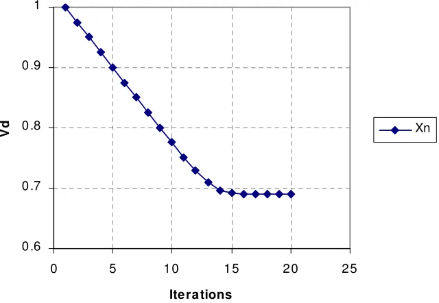
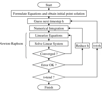
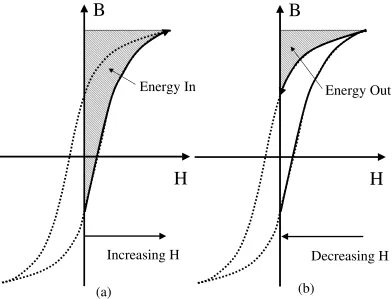
(10) List of Figures Figure 1.1 : Example system to be simulated.................................................................................... 7 Figure 1.2 : Project Structure ............................................................................................................ 8 Figure 2.1 : General Model Concept............................................................................................... 14 Figure 2.2 : Signal Flow and Conserved Energy Model Examples ................................................ 15 Figure 2.3 : Winding Model............................................................................................................ 19 Figure 2.4 : Simple Linear Network ............................................................................................... 22 Figure 2.5 : General Form of Netlist Entry ..................................................................................... 23 Figure 2.6 : SPICE Netlist for example circuit with realistic values ............................................. 23 Figure 2.7 : Non-Linear Diode Circuit Example............................................................................. 24 Figure 2.8 : Graph of the Diode Voltage, Vd (Xn), showing convergence to 0.69V ...................... 24 Figure 2.9 : Time Domain Analysis Flowchart............................................................................... 28 Figure 3.1 Scanning Electron Microscope (SEM) Image of Philips 3F3 soft ferrite material with a magnification of 1,400 showing ferrite grains. ...................................................................... 32 Figure 3.2: Progressive alignment of magnetic domains and grains, and the resulting magnetization curves for applied field strength H ......................................................................................... 32 Figure 3.3: Types of Magnetization Curve and Hysteresis Loop.................................................... 34 Figure 3.4: Anhysteretic Magnetization Curve ............................................................................... 35 Figure 3.5: Major BH Loop showing basic set of metrics .............................................................. 36 Figure 3.6: (a) Energy In due to increasing Applied Field (H) (b) Energy Out due to decreasing Applied field (H) .................................................................................................................... 37 Figure 3.7: Minor Loop Relaxation Curves .................................................................................... 38 Figure 3.8: First Order Reversal Curves ......................................................................................... 39 Figure 3.9: Rayleigh Hysteresis Loop............................................................................................. 41 Figure 3.10: Jiles & Atherton Reversible and Irreversible Magnetization...................................... 42 Figure 3.11: Simple Magnetic Dipole............................................................................................. 45 Figure 3.12: Preisach Triangle ........................................................................................................ 46 Figure 3.13 : Preisach Diagram Initial Condition ........................................................................... 46 Figure 3.14: Changes in the Preisach Triangle due to changes in applied field direction .............. 47 Figure 4.1: Magnetic Material Test Bench Configuration .............................................................. 54 Figure 4.2: Voltage to Current Driving Circuit Schematic ............................................................. 54 Figure 4.3: Virtual Scope User Interface ........................................................................................ 56 Figure 4.4: Philips 3F3 Family of Measured BH Curves................................................................ 57 Figure 4.5: First Order Reversal Curves ......................................................................................... 58 Figure 4.6: Original Jiles Atherton Model Structure....................................................................... 59 Figure 4.7: Original Jiles-Atherton PSPICE model listing ............................................................. 59 Figure 4.8: PSPICE BH Curve showing a major loop .................................................................... 60 ix.
(11) Figure 4.9: Electro-Magnetic Model of a non-linear inductor using PSPICE ................................ 61 Figure 4.10: Piece-Wise Linear Function for Jiles-Atherton variable - δ ....................................... 62 Figure 4.11: Measured BH curve showing closure at loop tips ...................................................... 63 Figure 4.12: Modified Jiles-Atherton model with field strength limit and Flux slope modifications ................................................................................................................................................ 64 Figure 4.13: Minor Loop (35 A/m) Optimization Results .............................................................. 66 Figure 4.14: Medium Field Strength (70A/m) Optimization Results ............................................. 67 Figure 4.15: Major Loop (140 A/m) Optimization Results ............................................................ 68 Figure 4.16: Measured, original and modified Jiles-Atherton BH curves ...................................... 69 Figure 4.17: Basic Magnetic Material metrics ................................................................................ 70 Figure 4.18: Polar Diagram showing Optimized and Measured Metrics........................................ 71 Figure 4.19: Measured, Least Squares and Metric Based Simulated BH Curves ........................... 73 Figure 4.20: Measured and Simulated Metrics Virtual Scope Screen ............................................ 74 Figure 4.21: Metric Weighting Function Implementation in Virtual Scope ................................... 75 Figure 4.22 : Virtual Scope Optimization Process Diagram........................................................... 76 Figure 4.23 : Univariate Search Method ......................................................................................... 77 Figure 4.24 : Flowchart of Simulated Annealing Method .............................................................. 79 Figure 4.25 : Flowchart of the Genetic Algorithm.......................................................................... 80 Figure 4.26: Comparison of Simulated Annealing and Genetic Algorithm Error Functions.......... 81 Figure 4.27: Comparison of measured, optimized original Jiles-Atherton model and optimized modified Jiles-Atherton model BH curves ............................................................................. 82 Figure 4.28: Statistical Comparison of the performance of the Simulated Annealing and Genetic Algorithm Approaches ........................................................................................................... 83 Figure 4.29: Multiple Loop Optimization Results for Siemens N30 (Major Loop) ....................... 84 Figure 4.30: Multiple Loop Optimization Results for Siemens N30 (Medium Loop).................... 84 Figure 4.31: Multiple Loop Optimization Results for Siemens N30 (Minor Loop) ....................... 85 Figure 4.32: Measured, original and Λ modified Jiles-Atherton BH Loops ................................... 87 Figure 4.33: Obtaining the Turning Points of H in the Jiles-Atherton model................................. 88 Figure 4.34: Dynamic BH Loop Major and Minor Loops .............................................................. 89 Figure 5.1 : Ideal Winding Model................................................................................................... 92 Figure 5.2: Flux paths showing Leakage Flux ................................................................................ 93 Figure 5.3: Simple, Bi-Filar, Split Bobbin and Interleaved Windings............................................ 95 Figure 5.4: Equivalent circuit assumed for measurement of winding capacitance ......................... 97 Figure 5.5: Variation in conductor skin depth with frequency. ...................................................... 99 Figure 5.6: The effect of proximity on the magnetic field distribution in windings ..................... 100 Figure 6.1 : Electrical Magnetic Component Model - 2 Winding Transformer............................ 102 Figure 6.2: Mixed Technology Model - 2 Winding Transformer ................................................. 103 Figure 6.3 : Implementing Low Frequency Winding Loss in a transformer................................. 105 x.
(12) Figure 6.4: Implementing Leakage Inductance in a transformer .................................................. 105 Figure 6.5: Complex Impedance Leakage and Loss Winding Model........................................... 106 Figure 6.6: Basic Core Loss Implemented in the electrical and magnetic domains...................... 107 Figure 6.7: Laminations and Equivalent Core Loss Circuit Model ............................................. 108 Figure 6.8: Frequency Dependent Eddy Current Behavioural Model Structure........................... 109 Figure 6.9: Division of VHDL-AMS model into Entity and Architecture ................................... 111 Figure 6.10: Using different architectures in VHDL-AMS .......................................................... 111 Figure 6.11: VHDL-AMS Editor and Debugger........................................................................... 112 Figure 6.12: SaberMMP Magnetic Modeling Software................................................................ 114 Figure 7.1: Transformer Winding Structure.................................................................................. 117 Figure 7.2: Theoretical and empirical leakage inductance variation with frequency.................... 118 Figure 7.3: Simple 2D Transformer Model................................................................................... 119 Figure 7.4: Simple 2D Finite Element Model ............................................................................... 120 Figure 7.5: 2D model using individual Layers.............................................................................. 121 Figure 7.6: Layer by Layer 2D Finite Element Model.................................................................. 121 Figure 7.7: Turn by Turn 2D Model ............................................................................................. 122 Figure 7.8: Turn by Turn 2D Finite Element Model..................................................................... 123 Figure 7.9: UOM2T Model Leakage Inductance Calculation....................................................... 124 Figure 7.10: Electro-Magnetic Transformer Model...................................................................... 125 Figure 7.11: Modified model of leakage reluctance ..................................................................... 125 Figure 7.12: Proposed Leakage Inductance Model in the electrical domain ................................ 126 Figure 7.13: Test Circuit for transformer, including the modified leakage inductance model, implemented in Spice ........................................................................................................... 127 Figure 7.14: Measured and Simulated leakage Inductance for RM12 transformer ...................... 127 Figure 7.15: Measured and Simulated leakage Inductance for RM10 transformer ...................... 128 Figure 8.1: XSPICE-FEA Model Structure .................................................................................. 131 Figure 8.2 : Spice-SLIM FE Analysis Procedure.......................................................................... 132 Figure 8.3: Slim-XSPICE test circuit netlist ................................................................................. 133 Figure 8.4: SLIM-XSPICE inductor schematic ............................................................................ 133 Figure 8.5: SLIM inductor FEA Mesh.......................................................................................... 134 Figure 8.6: Inductor Current and Voltage ..................................................................................... 134 Figure 8.7: Vector Plot of Flux Density in Core Corner............................................................... 135 Figure 8.8: SPICE-SLIM Inductor in Switch Mode Power Supply.............................................. 136 Figure 8.9: SPICE Netlist for Switch Mode Power Supply .......................................................... 136 Figure 8.10: Output Voltage Waveform of SPICE-SLIM simulation of switch mode power supply .............................................................................................................................................. 137 Figure 8.11: Current drawn from the supply during SPICE-SLIM simulation of switch mode power supply ........................................................................................................................ 137 xi.
(13) Figure 9.1: Modification to the Jiles-Atherton model including temperature dependence........... 140 Figure 9.2 : Recovered and Dissipated Energy in the BH Loop ................................................... 142 Figure 9.3: Spice Listing of Jiles-Atherton model extended to include parameter variations with temperature........................................................................................................................... 143 Figure 9.4: Winding model with thermal pin connection ............................................................. 144 Figure 9.5: Thermal Convection Model........................................................................................ 146 Figure 9.6: Thermal Emission Model ........................................................................................... 146 Figure 9.7: Thermal Circuit........................................................................................................... 147 Figure 9.8: TN10/6/4 Physical Dimensions .................................................................................. 148 Figure 9.9: Test Configuration for Temperature Characterization................................................ 148 Figure 9.10: BH Characteristic variation with temperature .......................................................... 149 Figure 9.11: Variation of A with Temperature optimized to within 3% error ............................. 149 Figure 9.12: Variation of C with Temperature optimized to within 10% error ........................... 150 Figure 9.13: Variation of K with Temperature optimized to within 5% error ............................. 150 Figure 9.14: Variation of MS with Temperature optimized to within 5% error ........................... 151 Figure 9.15: Variation of Alpha with Temperature optimized to within 5% error ....................... 151 Figure 9.16: Magnetic Material Model Static Temperature Test Circuit in PSPICE.................... 152 Figure 9.17: Measured and Simulated BH Curves at 27ºC........................................................... 152 Figure 9.18: Measured and Simulated BH Curves at 95ºC........................................................... 153 Figure 9.19: Measured and Simulated BH Curves at 154ºC......................................................... 153 Figure 9.20: Electrical-Thermal-Magnetic Transformer Model in PSPICE ................................. 154 Figure 9.21: Measured and Simulated Transformer Secondary Voltage at 27ºC ......................... 154 Figure 9.22: Measured and Simulated Transformer Secondary Voltage at 70ºC ......................... 155 Figure 9.23. : Variation of B with time as Core Temperature Increases....................................... 156 Figure 9.24: Core Surface Temperature Rise for insulated core................................................... 157 Figure 10.1 : Basic Passive Fault Current Limiter ........................................................................ 158 Figure 10.2: Fault Current Limiter Operating Regions................................................................. 159 Figure 10.3 : Passive Fault Current Limiter Physical Configuration............................................ 160 Figure 10.4 : Proposed Model Structure ....................................................................................... 161 Figure 10.5 : Basic Permanent Magnet Model.............................................................................. 161 Figure 10.6 : Linear Permanent Magnet Model ............................................................................ 162 Figure 10.7 : Permanent Magnet Demagnetization Curve ............................................................ 162 Figure 10.8: Permanent Magnet Model based on the Langevin Function .................................... 163 Figure 10.9 : Illustration of Magnetic Recoil Trajectory .............................................................. 163 Figure 10.10: FCL Averaged BH and Impedance Curves ............................................................ 164 Figure 10.11 : FCL Based on TN29/19/17.6-3F3 Toroid ............................................................. 166 Figure 10.12: FCL Sensed Line Current and Secondary Voltage................................................. 167 Figure 10.13: BH Curve derived from FCL operation under nominal load conditions ................ 167 xii.
(14) Figure 10.14: FCL Sensed Line Current and Secondary Monitor Voltage Waveforms ............... 168 Figure 10.15: BH Curve for FCL under increased Line Voltage Conditions ............................... 168 Figure 10.16: FCL BH Curve under Fault Conditions (Load = 0.5Ω).......................................... 169 Figure 10.17: Measured and Simulated BH Curves...................................................................... 170 Figure 10.18: Measured and Simulated Flux Densities ................................................................ 170 Figure 10.19 : Modified Magnet Model with Frequency Dependent Reluctance......................... 171 Figure 10.20: Flux Density of the FCL with corrected phase shift............................................... 172 Figure 11.1: ADSL Network Configuration Outline .................................................................... 174 Figure 11.2: ADSL Bandwidth Allocation ................................................................................... 175 Figure 11.3: ADSL Analogue Interface ........................................................................................ 176 Figure 11.4 Transformer Insertion Loss with non-ideal model .................................................... 176 Figure 11.5 : Transformer Model Used for Simulation of Insertion Loss .................................... 177 Figure 11.6: Simulated Insertion Loss using Pspice ..................................................................... 177 Figure 11.7 : Simulated bandwidth increase with increasing Magnetising Inductance ................ 178 Figure 11.8 : Simulated increase in Insertion Loss with Winding resistance ............................... 178 Figure 11.9: Simulated decrease in bandwidth with increasing Leakage Inductance................... 178 Figure 11.10: Non-Linear BH Behaviour in Transformer Core.................................................... 182 Figure 11.11: Transformer THD Test Circuit ............................................................................... 184 Figure 11.12: Pspice Transformer THD Test Circuit.................................................................... 184 Figure 11.13: TN10/6/4-3E5 Comparison of Measured and Simulated THD .............................. 185 Figure 11.14 : ER11-3E6 Comparison of Measured and Simulated THD.................................... 186 Figure 11.15: ER11-3E6 Ungapped Core (20 turns) Measured vs Simulated THD..................... 187 Figure 11.16 : ER11-3E6 gapped Core (20 turns) Measured vs Simulated THD......................... 188 Figure 11.17: ER11-3E6 Gapped and Un-gapped Core Simulated BH Curves............................ 188 Figure 11.18: IIC Construction Details......................................................................................... 191 Figure 11.19: IIC and APC41199 THD versus Input Voltage @ 10kHz...................................... 192 Figure 11.20: IIC and APC41199 THD versus Input Voltage @ 100kHz.................................... 193 Figure 11.21: Planar PCB Construction........................................................................................ 194 Figure 11.22: E18 and APC41199 THD versus Input Voltage @ 10kHz..................................... 196 Figure 11.23: E14 and APC41199 THD versus Input Voltage @ 10kHz..................................... 197 Figure 11.24 : Measured Insertion Loss for APC41199, E14 and E18 based transformers ......... 198 Figure 11.25 Measured Parameters for APC41199 transformer vs Frequency ............................ 199 Figure 11.26 : Measure and Simulated Insertion Loss for APC41199 ......................................... 200 Figure 11.27 Measured Parameters for E14 transformer vs Frequency........................................ 200 Figure 11.28 : Measure and Simulated Insertion Loss for E14..................................................... 201 Figure 11.29 Measured Parameters for E14 transformer vs Frequency........................................ 202 Figure 11.30 : Measure and Simulated Insertion Loss for E18..................................................... 202 Figure 11.31: IMD Test Circuit .................................................................................................... 203 xiii.
(15) Figure 11.32: Measured Frequency Spectra for APC41199 with two tone input ......................... 204 Figure 11.33: Simulated Frequency Spectrum for APC41199 with two tone input ..................... 204 Figure 11.34 : Block Diagram of ADSL Hybrid Channel ............................................................ 206 Figure 11.35 ADSL Electronic Hybrid Circuit ............................................................................. 206 Figure 11.36: two-wire to four-wire hybrid schematic diagram ................................................... 207 Figure 11.37: APC78155 Measured and Simulated Transmit to Line Transfer Function ............ 209 Figure 11.38: APC78155 Measured and Simulated Transmit to Receive Transfer Function....... 209 Figure 11.39: APC78155 Line Transfer Function (measured, ideal and parasitic model)............ 210 Figure 11.40: Insertion Loss Simulation Results over 100 runs ................................................... 211 Figure 11.41: High Pass Response –3dB point over 100 simulation runs .................................... 212 Figure 11.42 Histogram of High Pass Response –3dB point........................................................ 212 Figure 11.43: Insertion Loss over 100 Monte Carlo Simulation Runs ......................................... 213 Figure 11.44: Correlation between insertion loss and winding resistance (rw) ............................ 213 Listing A.1: Spice Winding Netlist............................................................................................... 243 Listing A.2: Spice winding_th Netlist........................................................................................... 243 Listing A.3: Spice core Netlist ...................................................................................................... 243 Listing A.4: Spice classicja Netlist ............................................................................................... 244 Listing A.5: Spice classicja2 Netlist ............................................................................................. 245 Listing A.6: Spice classicja4 Netlist ............................................................................................. 245 Listing A.7: Spice xfr3 Netlist ...................................................................................................... 245 Listing A.8: Spice xfr4 Netlist ...................................................................................................... 246 Listing A.9: Spice xfr3_4a11 Netlist ............................................................................................ 246 Listing A.10: Spice vdslxfr3rx Netlist .......................................................................................... 246 Listing A.11: Spice vdslxfr3rx Netlist .......................................................................................... 247 Listing A.12: Spice expja Netlist .................................................................................................. 247 Listing A.13: Spice expja2 Netlist ................................................................................................ 248 Listing A.14: Spice thermalja Netlist............................................................................................ 249 Listing A.15: Spice Expja_th7 Netlist .......................................................................................... 250 Listing A.16: Spice Emission Netlist ............................................................................................ 250 Listing A.17: Spice Rconv Netlist ................................................................................................ 250 Listing A.18: Spice ctherm Netlist................................................................................................ 251 Listing A.19: Spice rtherm Netlist ................................................................................................ 251 Listing A.20: Spice pmlang Netlist............................................................................................... 251 Listing A.21: Spice pmagnet Netlist ............................................................................................. 251 Listing A.22: Spice pmagnet2 Netlist ........................................................................................... 251 Listing B.1 Saber Mast Jiles-Atherton (Gaussian k) coreja Model Listing .................................. 253 Listing B.2 : Saber MAST Original Jiles-Atherton Model coreja2 Listing .................................. 254 Listing B.3: Saber MAST Jiles-Atherton with minor loop extensions coreja3 Model Listing..... 256 xiv.
(16) Listing B.4: Saber MAST Jiles-Atherton with thermal extensions coreja_th Model Listing ....... 257 Listing C.1 : VHDL-AMS Core Entity Model Listing ................................................................. 258 Listing C.2 : VHDL-AMS Linear Core Architecture Model Listing............................................ 258 Listing C.3 : VHDL-AMS Non-Linear Langevin Core Architecture Model Listing ................... 259 Listing C.4 : VHDL-AMS Jiles-Atherton Core Entity Model Listing.......................................... 259 Listing C.5 : VHDL-AMS Jiles-Atherton Architecture Model Listing ........................................ 261 Listing C.6 : VHDL-AMS Winding Model Listing...................................................................... 262 Figure D.1: Excerpt from ifspec.ifs file for FEA Inductor............................................................ 263 Figure D.2: cfunc.mod XSPICE FEA Inductor Code Model........................................................ 263 Figure D.3: SLIM FEA Control File – basic.cntl.......................................................................... 264 Figure D.4: Example SLIM post-processing control file.............................................................. 264 Figure E.1 : Planar Winding TCL/TK Gui.................................................................................... 265 Figure E.2 EAGLE script (automatically generated) .................................................................... 266 Figure E.3: Automatically generated PCB design for E18 planar winding .................................. 267 Figure E.4: Double Sided 2-Spiral PCB design for E18 planar winding...................................... 267 Figure E.5: E18 and APC41199 THD versus Input Voltage @ 10kHz ........................................ 268 Figure E.6: E18 and APC41199 THD versus Input Voltage @ 100kHz ...................................... 269 Figure E.7: Bifilar Layout Implementation................................................................................... 270 Figure E.8: E14 and APC41199 THD versus Input Voltage @ 10kHz ........................................ 270. xv.
(17) List of Tables Table 1.1: Application Model and Simulation Requirements........................................................... 3 Table 3.1 Divalent Transition Metals used in Soft Ferrites ............................................................ 31 Table 3.2 Definition of Magnetic Material Metrics ........................................................................ 36 Table 3.3: Summary of Models and Requirements......................................................................... 51 Table 4.1 : Comparison of Metrics and Least Squares Optimized Parameters and Metrics ........... 73 Table 4.2: Comparison of Simulated Annealing and Genetic Algorithm Optimization with and without Gaussian k ................................................................................................................. 81 Table 6.1: List of Spice building block models ............................................................................ 110 Table 6.2 : Saber Model List and Descriptions............................................................................. 111 Table 6.3 : VHDL-AMS models and descriptions........................................................................ 113 Table 9.1: Measured and Simulated Temperature Rises............................................................... 155 Table 11.1: 3E5 model parameters................................................................................................ 184 Table 11.2: ER11-3E6 model parameters ..................................................................................... 186 Table 11.3: ER11-3E6 model parameters ..................................................................................... 187 Table 11.4: Table of core factors and winding area parameters ................................................... 194 Table 11.5: Measured and Simulated third order IMD products and input signals ...................... 205. xvi.
(18) Acknowledgements I would like to express my appreciation for the people who have contributed to the production of this thesis in a variety of ways. Firstly I would like to express my gratitude to Dr Neil Ross for supervising this project. His guidance has been instrumental in ensuring that the scope of the project has been kept within reasonable bounds. I also thank Professor Alan Evans for agreeing to be the internal examiner for this thesis. His comments have helped greatly with the development of the structure of the thesis. I have always appreciated the opportunity to study on this course and for this my thanks go to Professor Andrew Brown for allowing me to study in his group. As a mature student I am grateful for the financial assistance provided by the Engineering and Physical Sciences Research Council (EPSRC) and the CASE award provided by Advanced Power Components Ltd, Rochester, Kent. Without this support I would have been unable to undertake this course of study. I also acknowledge the moral and technical support given by Alstom Research and Technology Centre (ART) in Stafford, who provided software free of charge for use on this project, and my former colleagues at Avant! Corporation. Finally, and most importantly, I wish to express my sincere thanks to my family and friends. Without the support and understanding of my wife, Caroline, this work could not have taken place. It is also important to keep perspective, and in this regard my children, Nathan and Heather, have been instrumental. I also owe a debt of gratitude to my parents for providing me with the education to get this far. Sincere thanks also go to Alan Abernethy and my father for agreeing to proof read the manuscripts.. xvii.
(19) Declaration. I declare that the work in this thesis is entirely my own unless otherwise stated.. Peter Reid Wilson, November 2001. xviii.
(20) List of Abbreviations A.C.. Alternating Current. ADSL. Asymmetric Digital Subscriber Line – A form of High Speed Digital Communication. AHDL. Analogue Hardware Description Language. CAD. Computer Aided Design. D.C.. Direct Current. EMC. Electro-Magnetic Compatibility. E.M.F.. Electro Motive Force. FDM. Frequency Division Multiplexing. FFT. Fast Fourier Transform. HDL. Hardware Description Language. HDSL. High-speed Digital Subscriber Line – A form of High Speed Digital Communication. Hysteresis. Non-linear behaviour of magnetic materials. IEEE. Institution of Electrical and Electronics Engineers. IL. Insertion Loss. IMD. Inter Modulation Distortion. ISDN. Integrated Subscriber Digital Network. Major Loop. Large Hysteresis Loop. Minor Loop. Small Hysteresis Loop. QAM. Quadrature Amplitude Modulation. SMPS. Switch Mode Power Supply. THD. Total Harmonic Distortion. VDSL. Very high-speed Digital Subscriber Line – A form of High Speed Digital Communication. VHDL. Very high-speed ASIC Hardware Description Language IEEE Standard 1076-1993. VHDL-AMS. VHDL plus Analogue and mixed signal extensions from IEEE Standard 1076.1-1999. xDSL. Generic Label for Digital Subscriber Line Technologies such as ADSL or VDSL. xix.
(21) Chapter 1 1 Introduction 1.1. Project Motivation and Goals. Over the last ten years there has been a significant increase in the use of computer simulation in the design of electronic circuits. Simulation has been used to replace prototyping to some extent, partially for a wide variety of printed circuit boards (PCB) and completely in the case of application specific integrated circuits (ASIC), primarily in order to reduce the development time for designs and hence the costs of the design cycle. It has also been recognized that the use of simulation enables tests to be undertaken on a design that would be impossible practically, prohibitively expensive or dangerous thereby providing potentially much greater insight into the design’s performance and reliability. This use of simulation for design performance prediction and optimization can be termed “Virtual Prototyping” – a prototype on the computer that can be modified and experimented in a similar fashion to a breadboard. Unfortunately, the use of simulation may not be completely accurate, as the accuracy of the results depends entirely on the models used for the individual components, and also the circuit as a whole (e.g. circuit parasitics). This is no different to the case of breadboard parasitics, which may be significantly different to the final production design. If the simulation results are to be relied on to any extent for performance prediction, it is crucial that the models used are accurate, appropriate for the results required, and used in the manner for which they were designed. It is therefore imperative that prior to attempting to model or simulate an electronic system, the simulation requirements for the system and individual models are thoroughly understood, especially the accuracy and range of operation. In this project, the modeling of magnetic components in electric circuits has been undertaken from the perspective of three different application areas, xDSL broadband transformer hybrids, Passive Fault Current Limiters (FCL) and Switch Mode Power Supplies (SMPS). Each of these application areas require different aspects of the magnetic component model to be considered in detail, and widely differing system simulations to be undertaken. As a result, the model requirements for each application will be different. In this project, therefore, the application model requirements have been analyzed, and modeling carried out to support the final system simulations and performance calculations. Existing work is built upon and extended in the areas of magnetic material modeling and characterization, model optimization, model implementation and system simulation using mixed signal simulation. By using appropriate models and techniques, each application has been modeled and simulated with the simulation results compared with measured test results at all stages to demonstrate the accuracy of the methods used. The overall primary goal of this project is 1.
(22) to provide a set of models, techniques and software tools that can be used to efficiently and accurately simulate a wide variety of magnetic components in a range of target applications. The resulting simulations should provide key performance indicators and replicate the behaviour of the target applications in a reasonable time. The specific objectives of this project are discussed in the remainder of this chapter. 1.2 1.2.1. Definition of systems to be simulated Identification of Target Application Areas. The target application areas that were chosen for this project are as follows: •. Passive Fault Current Limiters (FCL). •. ADSL/VDSL broadband hybrid transformers. •. Switch Mode Power Supplies (SMPS). These applications have been deliberately chosen to provide different modeling and simulation challenges in this project, which will be discussed in detail in the next section of this thesis. The wide use of magnetic components in SMPS design made the choice of this application an easy one, with significant areas of work still to be addressed. SMPS designers require models that are accurate and efficient to simulate, without extensive analysis or characterization. Specific modeling issues, such as thermal interactions and parasitics, provide opportunities for significant improvements to previous work. Passive Fault Current Limiters using inductors with some form of magnetic offset (either using windings or permanent magnets) provide different modeling challenges in an area that has been less widely investigated from a simulation perspective. While there are large common research areas with SMPS transformers, enabling similar modeling techniques to be applied, the requirements of the application simulation and model structure are quite different. The potential for original work in this unusual area was identified as high and therefore ideal for further research. The final application requires a quite different set of simulation and modeling criteria. Broadband hybrids (including signal transformers) are high speed, digital, low power and low distortion systems. Where the SMPS and FCL transformers need good modeling of hysteresis losses, the Broadband components operate at low powers and high speeds. The accurate modeling of very low levels of distortion across a wide bandwidth is required, with detailed knowledge of the parasitics and their interactions with the hybrid circuit behaviour. Most existing work in this area has used simple linear models, with limited investigation of the effects of material hysteresis (albeit small) on distortion, signal to noise ratios and inter-modulation. In this project, high power non-linear modeling techniques have been applied to small signal models effectively to provide greater insight into the non-linear behaviour of the small signal transformers.. 2.
Figure
+7


Outline
Definition of a Model
Methods of Testing Magnetic Materials
Dynamic Minor Loop Modeling
Leakage Inductance
Capacitance
Electrical vs Mixed Domain Modeling
Incorporating parasitic effects in magnetic component models
Magnetic Component Modeling Software
Extensions to Spice to interface to an External Finite Element Analysis Solver
Discussion of Convergence Issues
Related documents
This table shows that there were significant differences at level (0.01) between the mentioned responses of the research sample to question 4 with highest frequency given for
In that case, we can entertain the idea of preconscious processes forming the framework of our conscious experience of the perceived painting if we accept that the precon-
The NETteller solution is implemented in the Headquarters in Cyprus and currently addresses BoC (Cyprus) and BoC ( Greece) and BoC (Romania), with each bank having its own
Kirk Goehring West Tennessee Bank, a Div of Decatur County Bank Jackson. Holt Pritchett West Tennessee Bank, a Div of Decatur County
The low educational attainment levels of the labor force in Upper Egypt (especially in rural areas) in comparison to other regions, can explain the concentration of workers in
Moreover, research has repeatedly shown that impairment in inferencing skill is related to children’s reading comprehension difficulties (e.g. Cain & Oakhill, 1999; Cain,
If the fi le is manually entered, the LO must enter the lead, select the trusted advisor from the drop-down and hit before the referral partner can see it.. Upon logging in, all
POSITION APPLIED FOR: Production planner / Quality Control & Quality Assurance Engineer, Technical / Process / R&D Engineer, Urgent controller. Qualifications: 2 years
