University of Southampton Research Repository
ePrints Soton
Copyright © and Moral Rights for this thesis are retained by the author and/or other copyright owners. A copy can be downloaded for personal non-commercial
research or study, without prior permission or charge. This thesis cannot be
reproduced or quoted extensively from without first obtaining permission in writing from the copyright holder/s. The content must not be changed in any way or sold commercially in any format or medium without the formal permission of the
copyright holders.
When referring to this work, full bibliographic details including the author, title, awarding institution and date of the thesis must be given e.g.
GALLIUM AND TITANIUM DIFFUSED OPTICAL WAVEGUIDE DEVICES IN SAPPHIRE
Vasilis Apostolopoulos
A thesis submitted for the degree of Doctor of Philosophy
FACULTY OF ENGINEERING AND APPLIED SCIENCE OPTOELECTRONICS RESEARCH CENTRE
UNIVERSITY OF SOUTHAMPTON
UNIVERSITY OF SOUTHAMPTON ABSTRACT
FACULTY OF ENGINEERING AND APPLIED SCIENCE OPTOELECTRONICS RESEARCH CENTRE
Doctor of Philosophy
GALLIUM AND TITANIUM DIFFUSED OPTICAL WAVEGUIDE DEVICES IN
SAPPHIRE
by Vasilis Apostolopoulos
This thesis describes new methods to realise an integrated Ti:Sapphire laser using thermal ionic diffusion. Passive and active waveguides were fabricated by thermal diffusion of gallium and titanium ions in sapphire.
Theoretical simulations were established which describe the potential of planar Ti:Sapphire waveguide lasers and intracavity wavelength selection devices. A diffusion study of gallium, titanium and gallium/titanium co-doping is presented; the diffusion coefficient of gallium ions in sapphire was calculated to be 3.3x10⁻¹⁷ m2s-1 at 16000C and the diffusion coefficient of titanium ions in sapphire at 16000C was found to be 1.7x10⁻¹⁵ m2s-1.
CONTENTS
CHAPTER 1 INTRODUCTION
1.1 Introduction...1
1.2 Advantages of the waveguide geometry...1
1.3 Sapphire as a substrate material for integrated optics ...3
1.3.1 Rare-earth doped sapphire devices ...3
1.3.2 Ti and Cr doped integrated devices in Sapphire ...4
1.4 Waveguides in sapphire by ionic diffusion ...5
1.5 General overview of the thesis ...7
References to Chapter 1...10
CHAPTER 2 TI: SAPPHIRE WAVEGUIDE LASER: THEORY AND MODELLING 2.1 Introduction...15
2.2 Material characteristics of sapphire ...16
2.2.1 Sapphire as a mineral...16
2.2.2 Synthetic Sapphire and modern applications...17
2.2.3 Crystal structure of Sapphire ...17
2.2.4 Physical properties of Sapphire and Ti:Sapphire...18
2.2.5 Spectroscopy of Titanium doped sapphire...19
i ) Energy levels of the Ti3+ ion in sapphire...19
ii ) Characteristics of the Ti:Sapphire laser...21
2.3 Waveguide Theory...24
2.3.1 Asymmetric slab waveguide model ...24
2.3.3 Beam Propagation Method (BPM) ...30
2.4 Titanium Sapphire waveguide laser model...33
2.4.1 Waveguide laser description...33
2.4.2 Energy levels of Ti:Sapphire. ...34
2.4.3 Gain and threshold of the waveguide laser ...35
i ) Population inversion...36
ii ) Laser gain ...37
iii ) Threshold of the laser...38
iv ) Pump and signal mode sizes...39
v ) Waveguide losses and mirror reflectivities. ...40
vi ) Device length...42
2.4.4 Slope efficiency and waveguide losses...43
2.5 Integrated wavelength selection ...43
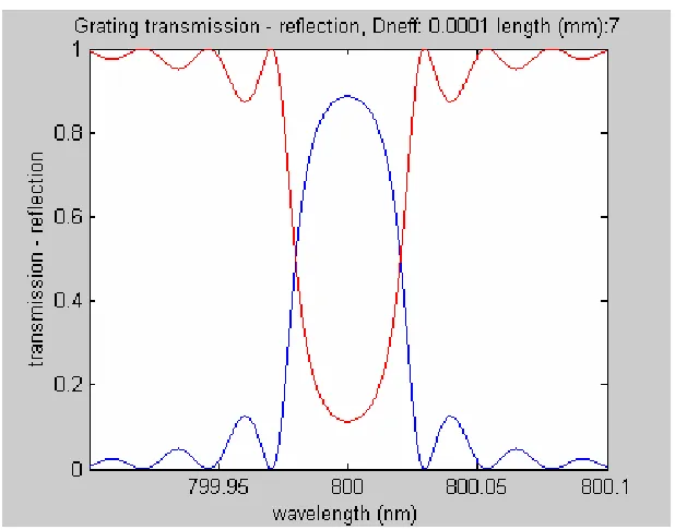
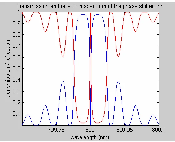
2.5.1 Grating wavelength selection...44
i ) F-Matrix model...45
ii ) Phase shifted grating ...47
iii ) Model results...48
2.5.2 Coupled cavity integrated resonators...51
i ) Basic principles of y-junction resonators ...52
ii ) Model for coupled cavity integrated resonators. ...54
iii ) Bent waveguides ...61
2.6 Conclusions...62
CHAPTER 3
DIFFUSION OF TITANIUM AND GALLIUM IN SAPPHIRE
3.1 Introduction...67
3.2 Theory of Diffusion ...68
3.2.1 Introduction...68
3.2.2 Mass flux and Fick’s first law...68
3.2.3 The diffusion equation ...69
3.2.4 Physical meaning of the diffusion coefficient. ...70
3.2.5 The Arrhenius relation ...71
3.2.6 Solutions to the diffusion equation. ...72
3.3 Overview of diffusion in sapphire ...74
3.3.1 Diffusion characterisation in sapphire ...74
3.3.2 Literature review of cation diffusion in sapphire...75
3.3.3 Review of titanium diffusion in sapphire...77
i ) Fabricated samples and characterisation techniques ...77
ii ) Concentration profiles of Ti in sapphire...79
3.3.4 Limitations of diffusion in sapphire...81
3.4 Diffusion of Gallium in sapphire...83
3.4.1 Introduction...83
3.4.2 Preparation of samples...84
3.4.3 Diffusion conditions...84
3.4.4 Characterization of diffusion profiles ...86
3.5 Combined Titanium and Gallium diffusion in Sapphire ...91
3.5.1 Introduction...91
3.5.2 Fabrication of samples ...92
3.5.4 Diffusion profiles of gallium and titanium diffused samples ...95
i ) Sample 1, Ti diffusion ...96
ii ) Sample 2, Ga diffusion followed by Ti diffusion...99
iii ) Sample 3, Ti diffusion followed by Ga diffusion...101
iv ) Sample 4, Ga/Ti diffusion ...103
v ) Overview of results for Ga/Ti diffusion ...105
3.6 Conclusions...106
References to Chapter 3...109
CHAPTER 4 GALLIUM DIFFUSED WAVEGUIDES IN SAPPHIRE 4.1 Introduction...111
4.2 Waveguide fabrication...112
4.2.1 Fabrication of slab waveguides...112
4.2.2 Fabrication of channel waveguides...113
4.2.3 Overview of fabrication parameters...114
4.3 Characterisation of Ga:Sapphire waveguides...115
4.3.1 Introduction...115
4.3.2 Experimental procedure for optical measurements...116
4.3.3 Mode profiles of samples 1 to 4 between wavelengths of 700 and 850nm. ...117
i ) Experimental results ...117
ii ) Discussion of results...120
4.3.4 Mode profiles of samples 5 to 8 at 488 and 633nm...122
4.3.5 Channel waveguide mode profiles...123
i ) Experimental results ...123
ii ) Discussion of results...124
4.4 Maximum index change of the Ga:Sapphire waveguides ...124
4.5 Conclusions...126
References to Chapter 4...128
CHAPTER 5
GALLIUM-DIFFUSED RIDGE WAVEGUIDES IN SAPPHIRE 5.1 Introduction...129
5.2 Fabrication ...130
5.2.1 Overview of the process...130
5.2.2 Details of SU-8 application...133
5.2.3 Fabricated samples...135
5.3 Characterisation of gallium diffused ridge waveguides ...136
5.3.1 Mode profiles...136
5.3.2 Prism coupling ...137
5.3.3 Propagation loss and spectral attenuation measurements ...138
5.4 Beam Propagation Model. ...141
5.5 Conclusions...143
References to Chapter 5...144
6.2 Ga and Ti diffused ridge waveguides ...146
6.2.1 Samples fabricated for characterisation of Ti and Ga co-diffusion. ...146
6.2.2 Experimental fluorescence configuration ...147
6.2.3 Fluorescence spectra of samples R1-R5 ...148
6.3 Ti:Sapphire ridge waveguide lasers...152
6.3.1 Fabrication overview of the titanium diffused ridge samples...152
6.3.2 Discussion of the fabrication procedure of the Ti-diffused ridge waveguides ...154
i ) Titanium diffusions ...154
ii ) SU 8 photolithography of the planar Ti:Sapphire waveguides ...154
iii ) Alignment and end-face polishing for active devices ...155
6.3.3 Characterisation of the Titanium sapphire ridges ...155
i ) Mode profiles and loss measurements...155
ii ) Fluorescence measurements ...156
iii ) Laser measurements ...158
6.3.4 Summary and discussion on the results of the waveguide lasers...161
6.4 Conclusions...164
References to Chapter 6...165
CHAPTER 7 CONCLUSIONS 7.1 Introduction...166
7.2 Summary of the presented work ...166
7.3 Proposed future research directions...168
7.3.1 Improvement of the Ti:Sapphire ridge waveguide laser...168
References to Chapter 7...171
ACKNOWLEDGMENTS
CHAPTER 1
INTRODUCTION
1.1
Introduction
The Ti:Sapphire laser was invented by Peter F. Moulton in 1982 [1,2] and quickly became commercially successful. Implementing the Ti:Sapphire laser in a waveguide geometry is expected to lead to a portable laser source with a tuning range from 650 to 1050nm with applications in spectroscopy, microscopy and sensing. This thesis describes the progress towards creating new methods to successfully realise active integrated devices in sapphire. In this thesis, fabrication of passive waveguides in sapphire by thermal diffusion of gallium is reported for the first time. Furthermore by micromachining the surface of the sapphire substrates ridge gallium diffused sapphire waveguides are fabricated and characterised for the first time. Finally using diffusion of titanium and surface micromachining the first rib waveguide titanium sapphire laser is realised.
1.2
Advantages of the waveguide geometry
phenomena. Nevertheless, the applications of the titanium sapphire laser are restricted because of the investment required to support such a system. A Ti:Sapphire laser system is expensive (50-100k£), partly because it requires an expensive pump laser (Argon Ion or frequency doubled solid state laser).
1.3
Sapphire as a substrate material for integrated optics
Since the first demonstration of the bulk Ti:Sapphire laser, research has been performed in order to use Al2O3 in integrated optics and a diversity of approaches has
been taken. Research was conducted aiming to realise a Ti:Sapphire laser in integrated geometry using a variety of fabrication methods [8-11]. There were also numerous attempts to use sapphire in bulk or film form as a host for other active ions [12]. There were successful attempts to grow Al2O3 films functioning as waveguides
on Si/SiO2 substrates for implementation of active integrated circuits with the
introduction of rare earth ions, such as erbium [13].
1.3.1 Rare-earth doped sapphire devices
Sapphire films have been demonstrated to form high quality passive waveguides and also have the potential for incorporating rare earth ions, Er, in high concentrations [13-16]. Due to the applications such as amplifiers in the telecommunications industry, there has been a great interest in research for the implementation of rare earth doping in Al2O3 films. The optical properties of rare earth ions are very weakly
dependent on the electric field of the host lattice as the electrons that undergo the laser transitions are in an inner energy shell. Consequently, the sapphire host films can be polycrystalline, which increases the freedom in the fabrication methods that can be used. Al2O3 films have been sputtered and subsequently doped using Er ion
1.3.2 Ti and Cr doped integrated devices in Sapphire
Similar scientific work has been carried out into the incorporation of Ti and Cr ions inside the lattice of sapphire using alternative methods. A significant difference between transition metal ions (Ti and Cr) and rare earths is that in the case of transition metals the laser electronic transition is in the outer shell which is strongly affected by the local crystal field. In the trivalent state the Ti3+ ion has the electron configuration of Ar]4s2 3d1, and can be regarded as a closed shell plus a single 3d
electron. The free space d-electron energy levels are five-fold degenerate (excluding spin) and there is no lower energy electron level to permit a radiative transmission. In the local crystal field of the sapphire the degeneracy is lifted and the levels are split thereby allowing laser transitions [24]. Consequently, single-crystal sapphire is needed as a host for these ions and the fabrication techniques are limited accordingly. At Southampton University work is being carried out into the fabrication of titanium sapphire waveguide lasers using pulsed laser deposition (PLD) [8,25,26]. A slab waveguide laser has been demonstrated using this technique, with 0.5W pump power threshold and fluorescence in ridge waveguides has been recently demonstrated using patterning and etching [27].
Another important approach, based on fibre geometry, aims at the fabrication of a low threshold, compact Ti:Sapphire source. A single crystal fibre was pulled using the laser heated pedestal method [11] and was operating as a Ti:Sapphire laser with 56nm of tuning range. Sapphire fibres are also important as probes, in sensing applications for measuring temperature in a wide temperature range, up to 18000C [45,46] and also in medical, surgical applications [47].
1.4
Waveguides in sapphire by ionic diffusion
Thermal diffusion is a promising fabrication process as it offers the potential for introducing a dopant inside a crystal without severely distorting the lattice of the host. The doping level and the depth of the diffusion can be controlled by appropriately selecting the parameters of the process such as time, temperature and thickness of the diffusion source. Diffusion in sapphire for fabrication of integrated devices is not thoroughly explored because until recently it was believed that in order to have the appropriate doping levels and diffusion depth required for waveguide fabrication forbiddingly high temperatures needed to be used. A first step towards this goal was achieved in the University of Southampton by Louise Hickey with the fabrication of the first Ti:Sapphire channel waveguide laser by thermal diffusion of titanium into a sapphire wafer [9,48-50]. The work presented here shows that titanium and gallium ions can be readily diffused to sufficient depths for waveguide fabrication [51,52].
gallium diffusion in sapphire is the strong component of surface diffusion. This poses a limit to the horizontal confinement that can be achieved in the fabrication of a channel waveguide using a patterned diffusion source. In this work a technological solution was developed, which is based on the surface micromachining of sapphire, after photolithography using SU-8 photoresist [52].
as the Ga3+ ion and passive diffused planar and ridge waveguides were fabricated and characterised [51,52,56].
Ga:Sapphire
waveguides Sapphire substrate
Tuning elements Ti-diffused region
Mirrors
Figure 1.1. Possible implementation of an integrated tunable titanium sapphire coupled cavity.
1.5
General overview of the thesis
given in order to investigate a cavity design which may be suitable for a Ti:Sapphire laser.
Chapter 3 describes the characterisation of the diffusion processes of titanium and gallium in sapphire. The chapter starts with the classical theory of diffusion as a theoretical basis for the characterisation of the results. The diffusion study of gallium, titanium and gallium/titanium codoping is presented in the chapter. Diffusion coefficients for all these cases are given and the results are discussed in terms of realising titanium and gallium integrated devices.
Chapter 4 describes the fabrication and characterisation of planar Ga:Sapphire passive waveguides; it starts with the description of the fabrication procedure for the waveguide samples. The characterization of the waveguide samples was based on a series of experiments which relate the fabrication parameters to the guided modes. The optimization of the samples was achieved by increasing the refractive index change and consequently minimizing the size of the mode waists. At the end of this chapter the results obtained in these experiments are used in waveguide models in order to conclude the characterisation of the waveguides.
Chapter 6 presents the realisation of the first Ti:Sapphire ridge waveguide lasers. The fabrication of the active devices is described and the experimental results giving the performance of the devices are given. The fabrication of sapphire circuits with titanium and gallium co-doping is included and fluorescence measurements on the waveguides are given.
Chapter 7 draws conclusions from the work presented in the thesis, and proposes future work which would exploit the devices realised in this project.
References to Chapter 1
1. P.F.Moulton. XXII Int. Quantum Electronics Conference. 1982. Munich, Germany.
2. P. F. Moulton, "Spectroscopic and Laser Characteristics of Ti-Al2O3," Journal
of the Optical Society of America B-Optical Physics 3, 125-133 (1986). 3. J. Goodberlet, J. Wang, J. G. Fujimoto, and P. A. Schulz, "Femtosecond
Passively Mode-Locked Ti-Al2O3 Laser with A Nonlinear External Cavity,"
Optics Letters 14, 1125-1127 (1989).
4. P. M. W. French, S. M. J. Kelly, and J. R. Taylor, "Mode-Locking of A Continuous-Wave Titanium-Doped Sapphire Laser Using A Linear External Cavity," Optics Letters 15, 378-380 (1990).
5. D. E. Spence, P. N. Kean, and W. Sibbett, "60-Fsec Pulse Generation from A Self-Mode-Locked Ti-Sapphire Laser," Optics Letters 16, 42-44 (1991). 6. Fasol G. "Room-temperature blue gallium nitride laser diode". Science 272,
1751. (1996).
7. Nakamura S. "Blue light emitting laser diodes". Thin solid films , 345. (1999). 8. A. A. Anderson, R. W. Eason, L. M. B. Hickey, M. Jelinek, C. Grivas, D. S.
Gill, and N. A. Vainos, "Ti:sapphire planar waveguide laser grown by pulsed laser deposition," Optics Letters 22, 1556-1558 (1997).
9. LMB Hickey, AA Anderson, and JS Wilkinson. "Ti:Sapphire channel
waveguide laser by thermal diffusion of titanium into sapphire. post deadline paper" pd6. 1997. Stockholm. 8th European Conference on Integrated Optics. 10. H. Lee, S. M. Lee, E. T. Ada, B. Kim, M. Weiss, S. S. Perry, and J. W.
Rabalais, "Shallow implantation of Ti+ ions in sapphire [alpha-
Al2O3(0001)]," Nuclear Instruments & Methods in Physics Research Section
B- Beam Interactions with Materials and Atoms 157, 226-232 (1999).
11. L. S. Wu, A. H. Wang, J. M. Wu, L. Wei, G. X. Zhu, and S. T. Ying, "Growth and Laser Properties of Ti-Sapphire Single-Crystal Fibers," Electronics Letters 31, 1151-1152 (1995).
12. G. N. vandenHoven, Snoeks, E., Polman, A., vanDam, C., vanUffelen, J. W. M., and Smit, M. K. "Optical gain in erbium-implanted Al2O3 waveguides."
Proc.of 7th European Conference on Integrated Optics, Delft, Holland , 229-232. 1995.
13. G. N. vandenHoven, R. J. I. M. Koper, A. Polman, C. vanDam, J. W. M. vanUffelen, and M. K. Smit, "Net optical gain at 1.53 μm in Er-doped Al2O3
14. G. N. vandenHoven, E. Snoeks, A. Polman, J. W. M. vanUffelen, Y. S. Oei, and M. K. Smit, "Photoluminescence Characterization of Er-Implanted Al2O3
Films," Applied Physics Letters 62, 3065-3067 (1993).
15. G. N. vandenHoven, E. Snoeks, A. Polman, C. vanDam, J. W. M. vanUffelen, and M. K. Smit, "Upconversion in Er-implanted Al2O3 waveguides," Journal
of Applied Physics 79, 1258-1266 (1996).
16. G. N. vandenHoven, J. A. vanderElsken, A. Polman, C. vanDam, K. W. M. vanUffelen, and M. K. Smit, "Absorption and emission cross sections of Er3+
in Al2O3 waveguides," Applied Optics 36, 3338-3341 (1997).
17. A. Polman, "Erbium implanted thin photonic films", Journal of Applied Physics 82, 1-39 (1997).
18. Muller R et al. "Spectroscopic study of the reduction of nickel and cobalt ions in sapphire." J.Chem.Phys 44, 365 (1966).
19. M. Mahnke, S. Wiechmann, H. J. Heider, O. Blume, and J. Muller, "Aluminum oxide doped with erbium, titanium and chromium for active integrated optical applications," Aeu-International Journal of Electronics and Communications 55, 342-348 (2001).
20. R. Serna, M. J. de Castro, J. A. Chaos, C. N. Afonso, and I. Vickridge, "The role of Er3+-Er3+ separation on the luminescence of Er- doped Al2O3 films
prepared by pulsed laser deposition," Applied Physics Letters 75, 4073-4075 (1999).
21. M. J. de Castro, R. Serna, J. A. Chaos, C. N. Afonso, and E. R. Hodgson, "Influence of defects on the photoluminescence of pulsed-laser deposited Er-doped amorphous Al2O3 films," Nuclear Instruments & Methods in Physics
Research Section B- Beam Interactions with Materials and Atoms 166, 793-797 (2000).
22. R. Serna, M. J. de Castro, J. A. Chaos, A. Suarez-Garcia, C. N. Afonso, M. Fernandez, and I. Vickridge, "Photoluminescence performance of pulsed-laser deposited Al2O3 thin films with large erbium concentrations," Journal of
Applied Physics 90, 5120-5125 (2001).
23. E. Alves, R. C. da Silva, M. F. da Silva, and J. C. Soares, "Solubility and damage annealing of Er implanted single crystalline alpha-Al2O3," Nuclear
Instruments & Methods in Physics Research Section B- Beam Interactions with Materials and Atoms 139, 313-317 (1998).
24. F.J.Duarte, Tunable lasers handbook, (Academic press, 1995).
26. M. Jelinek, R. W. Eason, J. Lancok, A. A. Anderson, C. Grivas, C. Fotakis, L. Jastrabik, F. Flory, and H. Rigneault, "Waveguiding pulsed laser deposited Ti : sapphire layers on quartz," Thin Solid Films 322, 259-262 (1998).
27. C. Grivas, D. P. Shepherd, T. C. May-Smith, R. W. Eason, M. Pollnau, A. Crunteanu, and M. Jelinek, "Performance of Ar+-milled Ti : sapphire rib waveguides as single transverse-mode broadband fluorescence sources," IEEE Journal of Quantum Electronics 39, 501-507 (2003).
28. Y. Saito, H. Kumagai, and S. Suganomata, "Coloration of Sapphire by Metal-Ion Implantation," Japanese Journal of Applied Physics Part 2-Letters 24, L880-L882 (1985).
29. A. P. Mouritz, D. K. Sood, D. H. Stjohn, M. V. Swain, and J. S. Williams, "Ion-Implantation of Low Melting-Point Metals Into Sapphire," Nuclear Instruments & Methods in Physics Research Section B- Beam Interactions with Materials and Atoms 19-2, 805-808 (1987).
30. T. Miyano, T. Matsumae, H. Yokoo, Y. Andoh, M. Kiuchi, and M. Satou, "Effect of High-Energy Ion-Implantation on Sapphire," Nuclear Instruments & Methods in Physics Research Section B- Beam Interactions with Materials and Atoms 59, 1167-1172 (1991).
31. Y. Saito, H. Horie, and S. Suganomata, "Coloration of Sapphire by Co Ion-Implantation," Nuclear Instruments & Methods in Physics Research Section B- Beam Interactions with Materials and Atoms 59, 1173-1176 (1991). 32. M. Bauer, S. M. M. Ramos, B. Canut, J. L. Loubet, L. Romana, L. Gea, P.
Kapsa, and P. Thevenard, "Titanium and Niobium Implantation Into Alpha-Al2O3 - Structural and Mechanical-Properties," Nuclear Instruments &
Methods in Physics Research Section B- Beam Interactions with Materials and Atoms 65, 301-304 (1992).
33. G. W. Arnold, "Ion-Implantation Effects in Al2O3 - Hydration and Optical- Absorption," Nuclear Instruments & Methods in Physics Research Section B- Beam Interactions with Materials and Atoms 80-1, 1036-1039 (1993).
34. E. Alves, M. F. daSilva, G. N. vandenHoven, A. Polman, A. A. Melo, and J. C. Soares, "Incorporation and stability of erbium in sapphire by ion
implantation," Nuclear Instruments & Methods in Physics Research Section B- Beam Interactions with Materials and Atoms 106, 429-432 (1995).
35. C. J. McHargue, J. D. Hunn, D. L. Joslin, E. Alves, M. F. daSilva, and J. C. Soares, "Etching of amorphous Al2O3 produced by ion implantation," Nuclear
Instruments & Methods in Physics Research Section B- Beam Interactions with Materials and Atoms 127, 596-598 (1997).
37. D. Z. Xie, D. Z. Zhu, H. C. Pan, H. J. Xu, and Z. X. Ren, "Enhanced etching of sapphire damaged by ion implantation," Journal of Physics D-Applied Physics 31, 1647-1651 (1998).
38. S. Nakao, M. Ikeyama, M. Tazawa, P. Jin, H. Niwa, S. Tanemura, Y.
Miyagawa, S. Miyagawa, and K. Saitoh, "High-energy co-implantation of Ti and O ions into sapphire," Materials Chemistry and Physics 54, 342-345 (1998).
39. J. C. McCallum and L. D. Morpeth, "Synthesis of Ti : sapphire by ion
implantation," Nuclear Instruments & Methods in Physics Research Section B- Beam Interactions with Materials and Atoms 148, 726-729 (1999).
40. J. Tian, Q. Z. Wang, Y. F. Chen, and Q. J. Xue, "Reaction in Al2O3 surface
layers upon ion implantation," Journal of Materials Chemistry 10, 565-569 (2000).
41. M. Ando, Y. Kanemitsu, T. Kushida, K. Matsuda, T. Saiki, and C. W. White, "Sharp photoluminescence of CdS nanocrystals in Al2O3 matrices formed by
sequential ion implantation," Applied Physics Letters 79, 539-541 (2001). 42. L. D. Morpeth and J. C. McCallum, "Ti : sapphire formation via the
co-implantation of Ti and O ions into sapphire," Nuclear Instruments & Methods in Physics Research Section B- Beam Interactions with Materials and Atoms 175, 537-541 (2001).
43. C. Marques, M. M. Cruz, R. C. da Silva, and E. Alves, "Optical changes induced by high fluence implantation of Co ions on sapphire," Surface & Coatings Technology 158, 54-58 (2002).
44. M. Ikeyama, S. Nakao, and M. Tazawa, "Optical property changes in sapphire induced by triple-energy Cu and O implantation," Surface & Coatings
Technology 158, 720-724 (2002).
45. Y. H. Shen, L. M. Tong, Y. Q. Wang, and L. H. Ye, "Sapphire-fiber
thermometer ranging from 20 to 1800 degrees C," Applied Optics 38, 1139-1143 (1999).
46. J. H. Sharp, C. W. P. Shi, and H. C. Seat, "Er-doped sapphire fibre
temperature sensors using upconversion emission," Measurement & Control 34, 170 (2001).
47. J. Fitzgibbon and G. Hayes, "Sapphire optical fibers: Rugged fiber expands surgical and sensor applications," Photonics Spectra 33, 118-119 (1999). 48. L. M. B. Hickey and J. S. Wilkinson, "Titanium diffused waveguides in
sapphire," Electronics Letters 32, 2238-2239 (1996).
50. Louise M.B.Hickey, PhD thesis, "Ti:Sapphire waveguide laser by the thermal diffusion of Ti into sapphire", (Optoelectronics Research Centre, University of Southampton, 1998).
51. V. Apostolopoulos, L. M. B. Hickey, D. A. Sager, and J. S. Wilkinson, "Gallium-diffused waveguides in sapphire," Optics Letters 26, 1586-1588 (2001).
52. V.Apostolopoulos, L.M.B.Hickey, D.A.Sager, and J.S.Wilkinson. "Gallium diffused ridge waveguides in Sapphire". CLEO Long Beach California. 2002. 53. Louise MB Hickey. "Report on Activities in Southampton during the 1851
fellowship award". 1999.
54. Becker P et al. "Er-Diffused Ti-LiNbO3 Wave-Guide Laser of 1563 and 1576
nm emission wavelengths". Applied Physics Letters 61, 1257 (1992).
55. R. Brinkmann, W. Sohler, and H. Suche, "Continuous-Wave Erbium-Diffused LiNbO3 Wave-Guide Laser," Electronics Letters 27, 415-417 (1991).
CHAPTER 2
T
I
:
S
APPHIRE WAVEGUIDE LASER
:
T
HEORY AND
M
ODELLING
2.1 Introduction
In this chapter the theoretical background to the different concepts surrounding the
realisation of active waveguide devices in sapphire is presented. Further, in order to
outline the potential performance of a Ti:Sapphire waveguide laser, theoretical
simulations were developed and the modelling results are given.
The chapter starts with an introduction of the fundamental material properties of pure
and doped sapphire. The basic physical properties of sapphire are given as well as its
chemical composition and crystal structure. Following this introduction to the
substrate material, the basic theory of the optical waveguide is included. A range of
waveguide models are described, starting with the simple theory of the slab
waveguide model and continuing with the description of increasingly complex and
powerful models. Subsequently basic laser theory is presented and in particular a
theoretical model of a 4-level laser system that is expanded into waveguide geometry.
This simulation analyses the potential performance of the integrated Ti:Sapphire laser,
In the final part of this chapter the potential for integrated wavelength selection
mechanisms is explored. The first configuration analysed is a Distributed FeedBack
laser (DFB) in which the wavelength selection element is a surface relief grating. The
theory of DFB lasers is presented with modelling results. The second possible
wavelength selection mechanism is a coupled cavity configuration in waveguide
geometry and is described using a novel theoretical analysis and simulation for the
specific device.
2.2 Material characteristics of sapphire
2.2.1 Sapphire as a mineral
Sapphire and ruby in mineral science are considered to be variations of corundum; the
chemical composition of corundum is Al2O3. Corundum is a very well documented
mineral and gemstone, which can be found in nature in a magnificent variety of
colours. Historically, corundum or sapphire is known as a precious stone. A very
important characteristic of sapphire is that it is the second hardest material that can be
found in nature after diamond and it is chemically inert to any etchant at room
temperature [1]. Sapphire rates 9 in the Moh scale; as a comparison, diamond rates 15
(definition of the scale’s maximum) and common glasses rate approximately 4 [1,2].
Sapphire is a very bright gemstone because of its high refractive index (~1.766 at
800nm) and high purity natural crystallisation. Mineral sapphire is a blue-coloured
corundum that takes its colour from the combination of iron and titanium ions. Ruby
2.2.2 Synthetic Sapphire and modern applications
Synthetically grown, single crystal sapphire without any dopants, appeared at the
beginning of the 20th century. Although sapphire is known in mineralogy as form of
corundum containing Ti and Fe ions, synthetic sapphire is single crystal Al2O3 also
known as α-alumina. The single crystal is hard, chemically inert, and has high
thermal conductivity and excellent electrical resistivity. These characteristics make
sapphire a successful insulating substrate for microelectronic components.
Furthermore it is an excellent material for fabrication of optical windows in
applications where robustness and high optical transmission is needed. Sapphire
became important in optoelectronics when ruby was reinvented as the first laser
material in 1960 [3]. Following this, in 1982 the Ti doped sapphire laser was
discovered by Peter F. Moulton, and very rapidly became a successful scientific laser
[4-6]. Due to this variety of applications, today high quality synthetic sapphire can be
readily obtained at relatively low prices (approximately £100), usually in wafer form
and surface polished to optical flatness.
2.2.3 Crystal structure of Sapphire
The crystal structure of sapphire can be simplified as a hexagonal close packed
structure. The lattice consists of layers of close packed oxygen ions with aluminium
sites between each oxygen plane. Only two out of every three aluminium sites are
occupied in order to preserve electrical neutrality. The exact description of the lattice
system of corundum is trigonal hexagonal Scalenohedral the point group symbol is
-3 2/m in international symbols or C3v in Schoeflies symbols; the space group of
sapphire is R3_c [1,2,7,8]. Figure 2.1 shows a sketch of the lattice of sapphire,
Figure 2.1. Lattice of sapphire, from [1,2].
2.2.4 Physical properties of Sapphire and Ti:Sapphire.
Sapphire is a uniaxial material with a weak negative birefringence, the extraordinary
refractive index being about 0.01 lower than the ordinary index at a wavelength of
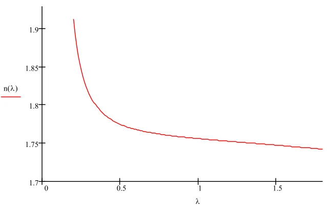
633nm [9]. The refractive index of sapphire is near 1.75 at visible wavelengths and in
Figure 2.2 a graph of refractive index versus wavelength is depicted. The refractive
index of sapphire in Figure 2.2 is calculated using the Sellmeier equation with the
appropriate parameters [1].
0 0.5 1 1.5
1.7 1.75 1.8 1.85 1.9
n( )λ
[image:29.595.103.422.499.704.2]λ
The refractive index of sapphire is dependent on stresses, defect concentration and
impurities. The dependency on impurities can be used as an advantage for the
realisation of waveguides in sapphire, by introducing dopants. Waveguides have been
fabricated in the course of this project using the diffusion of Ti and Ga ions [10-12].
Furthermore the refractive index of a Ti:Sapphire crystal increases with illumination
at blue-green wavelengths near the absorption of the active ion, Ti3+ [13,14]. The
refractive index also increases with temperature, which can have a significant effect
on the performance of a laser based on sapphire since it can result in thermal lensing
[15,16]. Generally Ti:Sapphire lasers are sensitive to heating and the performance of
the first fabrication attempts of Ti:Sapphire lasers was dependent on liquid nitrogen
cooling (77K) [17]. However the excellent heat conductivity of sapphire is convenient
for successful cooling of the device and at present commercial laser systems use water
cooling. In addition, the waveguide geometry is excellent for efficient conductive heat
extraction as the laser structure is near the surface of the substrate.
2.2.5 Spectroscopy of titanium doped sapphire.
i) Energy levels of the Ti3+ ion in sapphire
Single crystal sapphire is transparent from wavelengths of 200nm to about 7μm [1]; in
the optical region, characteristic absorptions occur when the crystal is doped with
metal ions, as in the cases of mineral sapphire and ruby. When sapphire is doped with
titanium ions, for the preservation of local charge neutrality the Ti3+ ion is
incorporated substitutionally in the Al sites. In the trivalent state the Ti3+ ion has the
electron configuration of Ar]4s2 3d1, and can be regarded as a closed shell plus a
single 3d electron. The free space d-electron energy levels are five-fold degenerate
transmission. In the local crystal field the degeneracy is lifted and the levels are split
thus allowing laser transitions [18]. The site of the trivalent titanium ion has trigonal-
and cubic- symmetry components [8,19,20]. The first splitting of the degenerate
energy levels of the 3d electron results from the cubic field that splits the energy
levels into a triply degenerate 2T2 ground state and a doubly degenerate 2E excited
state. The trigonal field splits the 2T2 ground state into two levels. The lower energy
level of the ground state, 2T2, is then split again by spin-orbit interaction. The doubly
degenerate 2E excited state is finally split by the dynamic Jahn-Teller effect. The
five-fold initial degeneracy of the free electron is completely lifted. In Figure 2.3 a
schematic diagram for the splitting of the energy levels is shown. The energy states of
the electron are coupled with phonon states, thus the transitions are significantly
broadened and Ti:Sapphire is considered to be a vibronic laser [18].
Free ion with 3d electron five- fold degeneracy
Splitting due to the cubic field
2E
2T 2
Trigonal field splitting
Spin-orbit splitting
Jahn-Teller splitting
Figure 2.3. A schematic diagram showing how the crystal field lifts the degeneracy of the energy
ii) Characteristics of the Ti:Sapphire laser
It can be observed that sapphire is an exceptional host for the Ti3+ ion; because of the
energy level splitting a laser transition is possible with the 2E→2T
2 transition. Data on
fluorescence for this transition was first reported by Gachter and Koningstein in 1974
[20] and the first Ti:Sapphire laser was reported, as mentioned, in 1982 by Moulton
[4]. In Figure 2.4 the characteristic absorption and emission spectra of Ti doped
sapphire is shown from [5]. The peak of the absorption curve is very near 488nm,
which is a characteristic line of an Argon ion laser. Typical pumping lasers for a
Ti:Sapphire system are Argon ion lasers and more recently CW frequency-doubled
solid state sources (Nd:YLF) are used. The π-polarisation is more strongly absorbing
than the σ-polarisation and the peak absorption cross-section is approximately 10-20
cm-2 [21].
Figure 2.4. Absorption and fluorescence spectra of Ti:Sapphire for the π-polarisation, from [5].
The titanium ions are incorporated in the crystal in the same sites resulting in the line
of each atom being broadened the same way, therefore Ti:Sapphire lasers can be
crystal demonstrates collision broadening which is a case of homogeneous broadening
and the lineshape of the transition is theoretically described by a Lorentzian
distribution [22] .
The peak of the emission curve is near 770nm and the most impressive characteristic
of the Ti:Sapphire laser is that the emission curve stretches over approximately
450nm, from 650nm to 1100nm. This bandwidth of 200THz makes the Ti:Sapphire
laser a very attractive tunable source with applications in spectroscopy, microscopy
and sensing. Furthermore, Ti:Sapphire systems are the most attractive solutions for
the generation of ultra-short pulsed sources, this is because the minimum duration of a
mode-locked pulse is inversely proportional to the bandwidth of the emission
spectrum. Mode-locked, Q-switched Ti:Sapphire lasers are used for the generation of
ultra-short pulses in the femtosecond and, recently, in the attosecond region [23-26].
These systems are used for white light generation and spectroscopy, observation of
ultra-fast phenomena and very demanding laser machining applications. The laser
linewidth increases with temperature as with most laser systems, for example ruby,
Nd:YAG etc. The product of the absorption cross-section and the emission lifetime is
considered to be a characteristic of the laser medium. The cross-section gives the
efficiency with which the pump radiation will raise an ion to the upper level and the
lifetime of the transition gives the available time for a successful population inversion
to happen. Therefore, a high σ⋅τ product indicates the potential for a low threshold
and high slope efficiency laser, as in the case of the Nd:YAG laser. The lifetime of a
laser transition is inversely proportional to the width of the line (FWHM), and for a
Therefore in the case of Ti:Sapphire the broadband spectrum indicates a trade-off in
the lifetime of the transition. The measured lifetime for Ti:Al2O3 lasers is
approximately 3μs at room temperature and as the lifetime decreases with
temperature, the linewidth increases [27].
The titanium ion in the sapphire lattice is in the trivalent state as it occupies the site of
a trivalent ion, aluminium. Due to lattice defects, it is probable that traces of Ti4+ exist
in the crystal. The ion induces a distortion in the lattice field and causes a shift of the
absorption of nearby Ti3+ ions towards the infrared. This shift in absorption results in
an overlap with the emission band of the laser [28,29]. Figure 2.5 shows the
absorption due to the Ti3+-Ti4+ pairs which can be seen to have a peak near 800nm.
This effect limits the performance of the laser as it increases the losses in the cavity.
An important characteristic of a titanium doped sapphire crystal is the ratio of peak
absorption in the blue-green region (488nm) and the parasitic peak absorption near
800nm. This ratio is called Figure of Merit (FOM) and characterises the quality of the
crystal, at present crystals with FOM near 1000 can be fabricated, although they are
highly priced.
Figure 2.5. Absorption spectra of Ti3+-Ti4+ pairs, from [5].
2.3 Waveguide Theory
In the previous sections the characteristics of sapphire as a material and the basic
spectroscopic characteristics of the Ti:Sapphire laser were presented. The aim of this
project is the realisation of diffused Ti:Sapphire ridge waveguide laser using gallium
or titanium as the waveguide ion and in this section the theory of optical waveguides
is presented. This section starts with the analysis of simple models and a geometrical
approach to the waveguide theory, continuing with increasingly complex models that
are sufficiently flexible to solve the more complex waveguide structures that are
studied in this project.
2.3.1 Asymmetric slab waveguide model
Light can be confined or guided in a material with higher dielectric coefficient than its
in which a thin layer has higher refractive index than the substrate material. Similarly,
in the case of optical fibre the core of the silica thin rod has a dopant that increases its
refractive index and is capable of supporting guided modes.
Guiding is based upon the phenomenon of total internal reflection (TIR). For angles
greater than a critical angle, light can be guided inside the structure. However, guiding
does not occur for all angles above the critical angle but for discrete angle values.
This gives rise to the presence of discrete guided modes, each waveguide mode
corresponding to one angle of reflection inside the structure. One way to understand
why only discrete angles can give guiding is to imagine the waveguide in the direction
vertical to the propagation direction as a cavity. In this cavity the incident and the
reflected wave should interfere constructively; that corresponds to only a set of angles
which give the correct path lengths in order for a stationary wave to be built.
The symmetric and asymmetric slab waveguide are the simplest models for analysis
of waveguide structures. The waveguide model presented here is based on an
approximation to a hypothetical Ga:Sapphire diffused waveguide. In this case the
simplest model that can be used is the asymmetric slab waveguide. Figure 2.6 shows a
sketch depicting the geometry of a Ga:Sapphire slab waveguide. The propagation
direction is along the z-axis and the TE-modes are polarized along the y-axis.
z x
Region 3: Sapphire ns=1.766
Region 2: Ga:Sapphire layer ng=ns+δn Region 1: Air, n=1
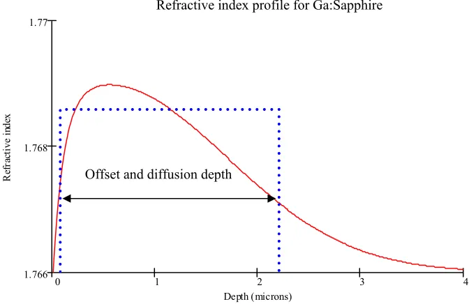
Waveguides created by diffusion do not have a step-like index profile assumed in the
development of the slab waveguide model. The index profile of the gallium and
titanium sapphire waveguides described in this thesis varies smoothly in a plane
perpendicular to the direction of propagation [10,12,30]. Nevertheless the profile may
be approximated by a step function, as shown in Figure 2.7.
0 1 2 3 4
1.766 1.768
[image:37.595.105.446.272.490.2]1.77 Refractive index profile for Ga:S
Figure 2.7. Step index approximation for a hypothetical Ga:Sapphire waveguide.
The basic equations of the slab waveguide model are derived, based on the analysis of
Donald L Lee [31]. In the slab waveguide an oscillatory behaviour in the core region
2 is assumed and exponentially decaying fields in regions 1 and 3 (Figure 2.6). The
field distribution for TE modes of the waveguide is assumed in the form
( )
jkzx a x x a y z x x e e A x k A e A z x E − − − ⎪ ⎪ ⎬ ⎫ ⎪ ⎪ ⎨ ⎧ + = 3 1 2 2 1 ) cos( , ψ 2 2 2 d x d x d x − < ≤ > (2.2) Depth (microns) R ef ract iv e i nd ex
Refractive index profile for Ga:Sapphire
Where the transverse wavenumbers are defined with the dispersion relation in each region 3 3 2 2 3 2 2 2 2 2 1 1 2 2 1 ε μ ω ε μ ω ε μ ω − = − = − = z x z x z x k a k k k a ( 2.3)
Continuing with these equations and taking boundary conditions at x=±d/2 for the
electric field of equation (2.2) and also for the magnetic field which is derived with
Maxwell’s curl equation the guidance condition for the TE modes of the waveguide is
derived,
π
p d
k TE TE
x 2
2 2 −Φ1 −Φ3 = where p = 0, 1, … (2.4)
Where the factor, , is the phase change of the field inside region 2 (waveguide
region). The other two factors are the phase change from total internal reflection at the
interface with the regions 1 and 3. The value of p represents different waveguide
modes; in general there is more than one solution to the equation for different
waveguide modes. The guidance condition for the TM modes is derived with the same
reasoning, and takes the same form with the phase changes on total internal reflection
but with different boundary conditions.
d
k2x
2
The guidance equation can be solved graphically or numerically and yields the
dispersion relation of the asymmetric slab waveguide. Three new quantities must be
introduced for the solution of the equation, a frequency parameter, v, normalized to
the film thickness that is defined by
(
2 3)
00 ε −ε ε
=k d
v where k0 ≡ω με0 (2.5)
the next parameter introduced is b, which is dependent on the effective index of the
(
ε −ε3)
(
ε2 −ε3)
= eff
b (2.6)
and finally an asymmetry measure α given by the relation
(
ε3 ε1)(
ε2 ε3)
α = − − (2.7)
With these normalizations introduced, a set of normalised curves for the first three TE
modes and for different asymmetry measures is depicted in Figure 2.8. It can be
observed that the fundamental mode for a symmetrical refractive index profile does
not have a cutoff, an example of this case is the index profile of an optical fibre.
[image:39.595.99.312.301.506.2]
Figure 2.8. Graphical solution of the guidance condition of a slab waveguide, from [31].
2.3.2 WKB method
Although the slab model is frequently used with graded-index waveguides, it can only
give precise results for waveguide structures that have a step index profile. The WKB
model is an efficient method to solve problems of graded-index waveguides. The
WKB method has the assumption that the guiding region is imbedded at a sufficient
buried only for 0.5μm. A WKB model was developed and the air-substrate index
profile discontinuity was lifted as the profile was generated using a logistic and not a
step function (Figure 2.7). Therefore the WKB model is used to compare with the
results of the slab model.
In a waveguide where the index variation is smooth, the boundaries of the guiding
region cannot be easily defined. However if they are found, then it is expected that the
field should oscillate within the boundaries or turning points and decay away
exponentially. In a WKB simulation the refractive index profile of the waveguides is
given as input and the modal effective indices are calculated with the following
equation [27,28].
( )
(
∫
b − = +a x
x n x neff dx p
k 2 2 0.5π
0
)
p=0, 1, 2, … (2.8)Where xa and xb are the turning points defined by the following relation.
( ) ( )
xa n xb neffn = = (2.9)
p is the number of the mode and n(x) is the refractive index profile. The algorithm
used tests the equality defined in equation (2.8) for different turning points and
effective refractive indices. This method is used in Chapter 3, with a refractive index
profile similar to the one depicted in Figure 2.7, for the calculation of the effective
indices of the slab Ga:Sapphire diffused waveguides.
2.3.3 Beam Propagation Method (BPM)
Beam propagation is a more sophisticated model that can deal with optical
propagation problems that have nearly arbitrary parameters. Waveguide channels
of ridge waveguides. These structures cannot be analysed with the methods described
above so that commercial BPM packages were used. Here the theory of the Beam
Propagation Method will be briefly described following the analysis of Reinhard
Marz and of Katsunari Okamoto [32,33]. The mathematical procedure used was
developed for underwater acoustics and seismology before it was adapted to optical
waveguide problems. BPM yields the response of a given device to an external optical
signal used as an input, in a way which closely parallels practical application.
The BPM is based in the forward Helmholtz equation which describes the propagation
of the optical field in respect to the propagation direction. The vector Helmholtz
equations are derived from Maxwell’s equations by eliminating the electric or
magnetic field. Solutions of the vector Helmholtz equations without a longitudinal
component are called transverse or scalar waves. In layered waveguide media two
types of scalar waves can be found, the transverse electric, usually referred as TE, and
the transverse magnetic, usually referred as TM.
For the electrical field the three-dimensional scalar wave equation (Helmholtz
equation), is given by
(
, ,)
02 2 2 2 2 2 2 2 = + ∂ ∂ + ∂ ∂ + ∂ ∂ E z y x n k z E y E x E (2.10)
The electric field can be separated into two parts,
) exp( ) , , ( ) , ,
(x y z x y z jkn0z
E =Φ − (2.11)
where the axially slowly varying envelope term is Φ(x, y, z) and the rapidly varying
term is exp(-jknoz), where n0 is the refractive index of the cladding. Substituting the
electric field in the Helmholtz equation yields,
(
)
Assuming the weakly guiding condition it can be approximated that
(
n −no)
≅2no(
n−no2
2
)
and equation (2.12) can be written as(
−)
Φ− Φ ∇ −
= ∂
Φ ∂
o n n jk kn
j z
2
0
2 (2.13)
When n=no only the first term of the right hand side will remain, which represents
free-space propagation in a medium having refractive index, no. The second term
gives the influence of the region having refractive index n(x, y, z). Both terms affect
simultaneously the propagation of light, however in BPM the influence of the two
terms is separated. Each term affects the light propagation separately and alternately
during the propagation step, Δz, furthermore during this step the dielectric profile is
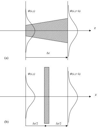
assumed to be constant. Figure 2.9 shows an example illustrating the operation of the
algorithm of the classical BPM. Figure 2.9 (a) shows light propagation in an actual
tapered waveguide and Figure 2.9 (b) shows the BPM simulation for light propagation
Δz
Δz/2 Δz/2
(b) (a)
Φ(x,z) Φ(x,z+h)
Φ(x,z) Φ(x,z+h)
z
[image:43.595.110.446.96.536.2]z
Figure 2.9. Schematic representation of the operation of a classical BPM algorithm.
In BPM analysis the field, Φ(x,y), is free-space propagated over a distance of Δz/2,
then the portrait of the field is corrected at the centre of propagation for the entire
distance, Δz, and again for a distance the field is propagated in free space. The
propagation of the optical field inside the waveguide is replaced by a sequence of free
very sensitive to the appropriate choice of propagation step. For small and smooth
index changes found in diffused waveguides the classical BPM is very successful but
for abrupt index changes (that can be found in semiconductor devices) cannot
successfully work except if a sufficiently small propagation step is chosen.
The method works like a simulated experiment, an optical field is launched inside the
waveguide and the efficiency of the coupling depends, as in real conditions, on the
overlap of the selected launch field with the waveguide supported modes. The optical
field is propagated until a stable state is reached and a solution for a waveguide mode
is obtained. If the length of propagation is not adequate or the launching field is not
appropriately selected the simulation will not give a solution for a supported mode.
This implies that results from a BPM model should be treated with more caution than
the other simulation methods presented.
A commercial simulation package called BeamProp was used for propagation
problems in planar and ridge waveguides created by ionic diffusion in sapphire.
Results of the BPM simulations will be shown in the following chapters.
2.4 Titanium Sapphire waveguide laser model
2.4.1 Waveguide laser description
In this section a model for a Ti:Sapphire laser system in a waveguide geometry is
derived. It is important to derive the relation of the expected laser threshold and gain
per unit length of this configuration, dependent on the waveguide characteristics
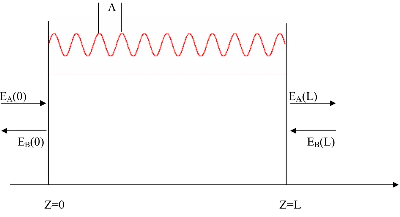
[22,34-36]. A schematic of a waveguide Ti:Sapphire laser is depicted in Figure 2.10.
using a microscope objective lens. The pump radiation and fluorescence is confined in
the waveguide region and plane dielectric mirrors provide the signal feedback at the
polished ends of the waveguides. The spectral characteristics of the mirrors are high
reflectivity at the signal wavelength (near 750nm) and high transmission at the pump
wavelengths. Once the total gain per round trip is higher than the losses of the
waveguide and of the mirrors, laser operation will commence.
Pump radiation
z
Channel waveguide
Mirrors
Laser radiation
Figure 2.10. Schematic for a Ti:Sapphire laser in waveguide geometry.
2.4.2 Energy levels of Ti:Sapphire.
Titanium has only one d electron, hence it is, at a first approximation a two-level
system that theoretically cannot lase since population inversion cannot be achieved.
However when Ti is incorporated into the lattice of sapphire each electron energy
level is coupled to lattice vibrations leading to splitting of the energy levels (section
2.2.5). Therefore Ti:Sapphire is a laser in a vibronic transition and operates as a
Figure 2.11. Energy levels and pumping scheme of a Ti:Sapphire laser.
The ground state, level 1, is a low vibrational state of the 2T2 electronic energy and, in
the presence of pump radiation, electrons are excited to level 2 which is an excited
vibrational state of the electronic level 2E. The electrons then undergo a rapid
non-radiative decay to a lower level of the state 2E, level 3. The transition from level 3 to
level 4 is the laser transition that can occur with stimulated emission. Level 4 is an
excited vibrational state of the 2T2 electronic energy level and the electrons follow a
non-radiative rapid decay back to level 1.
2.4.3 Gain and threshold of the waveguide laser
In this section a model is presented which describes how characteristics of the laser
such as threshold are dependent on characteristics of the configuration such as pump,
signal mode sizes of the waveguide, device length etc. A model is derived for this
4-level laser using the analysis of L. Hickey and M. Digonnet [22,35,36]; it is assumed
that the system is in thermal equilibrium, so that the rate of excitation is equal to the Level 1
Laser radiation (near IR)
2T
2 energy
levels
2Eenergy
levels
Level 2
Level 3
Level 4 Rapid decay
Rapid decay Pump radiation
rate of decay. The population of ions in level 1 is N0-N(x,y,z,t) where N0 is the
concentration of Ti ions in the substrate and N(x,y,z,t) is the number of excited ions.
Supposing that the depopulation of the ground state is negligible yields that
N(x,y,z,t)<<N0, therefore N0-N(x,y,z,t)≈ N0. Level 2, at any given moment, is assumed
to have negligible population because any ion in this state rapidly decays to level 3.
Level 3 is the level that holds the population of the excited ions, N(x,y,z,t). Level 4 is
also assumed to have negligible population because of the short lifetime of the excited
vibronic level.
i) Population inversion
Equation (2.14) gives the rate at which ions move from level 1 to level 3; this rate is
proportional to the intensity of the pump radiation, ion concentration, quantum
efficiency and absorption cross section of the transition.
p p h N z y x I dt dN ν ση 0 3 1 ) , , ( = → (2.14)
The laser transition rate from level 3 to level 4 has two components, the spontaneous
emission rate and the stimulated emission rate. It is assumed that for low pump
powers (up to threshold pump power) and for thermal equilibrium, the stimulated
emission rate is negligible. The spontaneous emission decay rate is given by the
following equation. τ ) , , ( 1 3 z y x N dt dN = → (2.15)
and in a thermal equilibrium state,
Therefore with this equation the population inversion of the laser may be estimated.
The intensity of the pump radiation is Ip(x,y,z) and that of the signal radiation is
Is(x,y,z). The intensities can be related to the power densities using the expression
I(x,y,z)= P(z)S(x,y), where the modal distributions of the pump and signal radiation in
the waveguide are Sp(x,y) and Ss(x,y) respectively, and are normalised such that
. Furthermore P(z) is the power of the signal or pump radiation.
Therefore using equation (2.16) and substituting the above expression for the pump
radiation yields,
∫ ∫
S(x,y)dxdy=1p p p h N (x,y) (z)S P z y x N ν τ ση 0 ) , ,
( = (2.17)
ii) Laser gain
The signal gain is the rate of growth of the signal due to the level of stimulated
emission and is proportional to the interaction of the incident signal Is(x,y,z), and the
population inversion, using the stimulated emission cross section.
) ( ) , , ( ) , , ( ) ( 0 z P FOM N dxdy z y x I z y x N dz z dP s p s s s s
∫∫
⎟⎟ ⎠ ⎞ ⎜⎜ ⎝ ⎛ + −= σ β σ (2.18)
The second term of equation 2.18 shows the loss due to the propagation loss of the
waveguide in signal wavelength and due to reabsorption of the signal due to Ti3+-Ti4+
pairs, which is given by the FOM. Substituting for the population inversion N(x,y,z)
and the intensity of the signal radiation
⎟ ⎟ ⎠ ⎞ ⎜ ⎜ ⎝ ⎛ ⎟⎟ ⎠ ⎞ ⎜⎜ ⎝ ⎛ + − =
∫∫
FOM N dxdy y x (x,y)S S (z) P h N z P dz z dP p s s p p p s p ss β σ
ν τ η σ
σ 0 0
) , ( ) ( ) ( (2.19)
The pump power, Pp(z), in the waveguide decays due to waveguide losses at the pump
wavelength and due to pump absorption from the Ti ions, assuming that the ground
) ) ( exp( ) 0 ( )
(z P N0 z
Pp = p − σp +βp (2.20)
In order to find an expression for the total gain in the waveguide laser equation (2.19)
has to be integrated over the length of the waveguide.
dz FOM N dxdy y x (x,y)S S (z)dz P h N z dP z P L p s s p L p p s p L P P s
s
∫
∫∫
∫
∫
= − ⎜⎜⎝⎛ + ⎟⎟⎠⎞ 0 0 0 0 ) ( ) 0 ( ) , ( ) ( ) (1 β σ
ν η σ τσ
(2.21)
Using equation (2.20), which gives the pump power as a function of the propagation
distance, and solving equation (2.21) yields,
(
)
∫∫
⎟⎟ ⎠ ⎞ ⎜⎜ ⎝ ⎛ + − + + − − = L FOM N dxdy y x (x,y)S S N P L N h NG p s s p
p p p p p p s
p β σ
β σ β σ ν η σ τσ 0 0 0 0 ) , ( ) 0 ( ) ) ( exp( 1
ln (2.22)
This equation gives the gain for the laser in which, the first term
p s p h N ν η σ τσ 0 , gives
the material characteristics, the second term
(
)
p p p p p N P L N β σ β σ + + − − 0
0 ) ) (0)
( exp( 1
describes the pump absorption, the integral
∫∫
Sp(x,y)Ss(x,y)dxdycalculates theoverlap of the waveguide modes at the pump and signal frequencies and finally the
last term L
FOM N p s ⎟⎟ ⎠ ⎞ ⎜⎜ ⎝ ⎛ + σ β 0
gives the loss of the signal wavelength due to the loss of the
waveguide and also due to signal reabsorption due to the Ti3+ and Ti4+pairs.
iii) Threshold of the laser
Using equation (2.22) the gain of the laser can be calculated as a function of the
device characteristics such as length, concentration and loss. The threshold pump
power is achieved when the gain is sufficient to overcome the extra loss of the
mirrors. Therefore the threshold will occur when
) ln(
Using equation (2.23), and solving equation (2.22) for the pump power, the
expression for the laser threshold is derived.
⎥ ⎦ ⎤ ⎢ ⎣ ⎡ − ⎟⎟ ⎠ ⎞ ⎜⎜ ⎝ ⎛ + + − − + =
∫∫
2 ) ln( ) , ( 1 ) ) ( exp( 1 2 1 0 0 0 0 R R L FOM N dxdy y x (x,y)S S L N N N h P p s s p p p p p s p p th σ β β σ β σ η σ τσ ν (2.24)In the following sections the expressions that give the gain and the threshold of the
laser will be analysed in order to determine how different characteristics of the system
affect the performance of the laser.
iv) Pump and signal mode sizes
As described above, the term is the overlap integral between
the waveguide modes at the signal and pump wavelengths. Assuming that the
waveguide has modes that can be approximated with concentric Gaussian functions
the normalised mode distribution at the pump wavelength can be written as
∫∫
Sp(x,y)Ss(x,y)dxdy⎥ ⎥ ⎦ ⎤ ⎢ ⎢ ⎣ ⎡ ⎟ ⎟ ⎠ ⎞ ⎜ ⎜ ⎝ ⎛ + −
= 1 exp 22 22
) , ( px py py px p w x w y w w y x S π (2.25)
where the waists are defined at 1/e of the maximum intensity. Then the solution for
the overlap integral is,
1 5 . 0 2 2 5 . 0 2 2 1 1 1 1 ) , ( ) , ( − ⎥ ⎥ ⎦ ⎤ ⎢ ⎢ ⎣ ⎡ ⎟ ⎟ ⎠ ⎞ ⎜ ⎜ ⎝ ⎛ + ⎟ ⎟ ⎠ ⎞ ⎜ ⎜ ⎝ ⎛ + =
∫∫
sy py sx px sy sx py px p s w w w w w w w w dxdy y x S y xS π (2.26)
In order to be able to describe the effect that the waveguide size will have on the gain
and threshold of the laser more clearly, the expression will be simplified by assuming
that the waveguide modes are not astigmatic, so that wpx=wpy=wp and wsx=wsy=ws, in
(
)
[
2 2]
1) , ( ) ,
( = + −
∫∫
Ss x y Sp x y dxdy π wp ws (2.27)Therefore equation (2.24) which gives the threshold of the waveguide can be writtern
as,
)
( 2 2
s p
th k w w
P = + ( 2.28)
where k is a proportionality constant. From this expression it is clear that the
threshold of the laser system is proportional to the square of the pump and signal
mode sizes. Therefore a waveguide with a smaller mode dimension will result in a
reduced threshold power. As expected, from equation (2.22) the gain of the laser is
also increased as the waveguide mode waists decrease. In the case of gallium diffused
waveguides in sapphire a mode size of 2μm is expected at the pump wavelength and
4μm at the signal wavelength [section 5.3.1]. In Figure 2.12 a plot of the gain of two
laser systems with different mode sizes is depicted, the graph indicates the importance
of mode size on the performance of a waveguide laser device.
0 10 20 30
2 4
trace 1 trace 2
length (mm)
Gain
(d
B) wp=2μm
ws=4μm
wp=4μm
ws=8μm
v) Waveguide losses and mirror reflectivities.
From the threshold equation of the laser, equation (2.24), it is clear that as the losses
of the waveguide at the signal and pump wavelength increase the laser threshold also
increases. Figure 2.13 shows the laser gain versus length for devices with increasing
propagation loss. The threshold of the laser decreases as the mirror reflectivities
increase, the value of the mirror reflectivity can be chosen so that it gives a low
threshold. Nevertheless high reflectivity mirrors will have a performance trade-off as
they reduce the slope efficiency. An important engineering consideration in a laser
device is the efficiency with which the mirrors couple the reflected radiation back in
the waveguide. Poor coupling of the reflected radiation increases the losses and
results in poor laser performance. Problems of bad coupling of the mirrors exist due to
mirror and waveguide separation, mirror tilt and curvature on the waveguide
end-faces. In Figure 2.14 threshold plots can be compared for devices that have the same
0 5 10 15 20 25 30
1 1 2 3 4 5
0 dB/cm loss 1 dB/cm loss 3 dB/cm loss Theoretical max
length (mm)
Gain (dBs)
Figure 2.13. Gain versus length, for waveguides with different loss, with a maximum theoretical
0 5 10 15 20 25 30 200
400 600 800 1000
Length (mm)
T
hr
eshold (
mW)
trace 1 trace 4
trace 2 trace 3
Loss (dB/cm) Reflectivity (%)
trace 1 0 90
trace 2 trace 3 trace 4
0 1 1
50 90 50
Figure 2.14. Threshold versus length for devices with different losses and mirror reflectivities
vi) Device length
In a waveguide without losses the threshold of the waveguide laser decreases as the
length of the cavity is increased. In Figure 2.14 for the two curves (trace 1 and 2)
representing a waveguide without propagation losses the threshold becomes minimum
as the length of the cavity becomes infinite. Conversely in a waveguide with
non-negligible propagation losses, which is the general case, the laser threshold becomes
minimum at an optimum length. In Figure 2.14 for traces 3 and 4, which represent
waveguides with 1 dB/cm losses, there is an optimum length (approximately 5 and
2.4.4 Slope efficiency and waveguide losses
The slope efficiency of the laser is defined as the rate of increase of the laser power
versus the launched pump power, above threshold. For a waveguide
![Figure 2.5. Absorption spectra of Ti3+-Ti4+ pairs, from [5].](https://thumb-us.123doks.com/thumbv2/123dok_us/1005809.615235/35.595.90.381.82.328/figure-absorption-spectra-of-ti-ti-pairs-from.webp)
![Figure 2.8. Graphical solution of the guidance condition of a slab waveguide, from [31]](https://thumb-us.123doks.com/thumbv2/123dok_us/1005809.615235/39.595.99.312.301.506/figure-graphical-solution-guidance-condition-slab-waveguide.webp)