Electron mobility of non-fullerene acceptors using a time of flight method Natalie A. Mica, Stuart A.J. Thomson, Ifor D.W. Samuel
PII: S1566-1199(18)30431-2 DOI: 10.1016/j.orgel.2018.08.027 Reference: ORGELE 4841
To appear in: Organic Electronics
Received Date: 27 June 2018 Revised Date: 2 August 2018 Accepted Date: 11 August 2018
Please cite this article as: N.A. Mica, S.A.J. Thomson, I.D.W. Samuel, Electron mobility of non-fullerene acceptors using a time of flight method, Organic Electronics (2018), doi: 10.1016/j.orgel.2018.08.027.
M
AN
US
CR
IP
T
AC
CE
PT
ED
Electron Mobility of Non-fullerene Acceptors Using a
Time of Flight Method
Natalie A. Mica, Stuart A. J. Thomson, Ifor D. W. Samuel
M
AN
US
CR
IP
T
AC
CE
PT
ED
1
Electron Mobility of Non-fullerene Acceptors Using a
Time of Flight Method
Natalie A. Mica, Stuart A. J. Thomson, Ifor D. W. Samuel
Organic Semiconductor Centre, SUPA, School of Physics and Astronomy, University of St Andrews, St Andrews, KY16 9SS, UK
Author email addresses:
M
AN
US
CR
IP
T
AC
CE
PT
ED
2
Abstract
Organic solar cells are a promising renewable energy technology, offering the advantages of mechanical flexibility and solution processability. The charge carrier mobility is an important parameter as it influences the competition between charge extraction and recombination and therefore the cell efficiency. We report the electron mobility of two high performance non-fullerene acceptors ITIC and IDTBR in neat films and blended with their common donors. In a pure film ITIC has a zero-field electron mobility of 7.4 x 10⁻⁴ cm2/Vs, which dropped to 1.0 x 10⁻⁴ cm2/Vs when put into a blend with PTB7-Th or P3HT. The IDTBR:P3HT blend was found to have a slightly lower electron mobility of 5.6 x 10⁻⁵ cm2/Vs. The measured electron mobility is the same order of magnitude as the hole mobility in these blends, leading to balanced transport and efficient photovoltaic cells.
M
AN
US
CR
IP
T
AC
CE
PT
ED
3
1. Introduction
M
AN
US
CR
IP
T
AC
CE
PT
ED
4
these materials create a well-balanced blend capable of even higher performance.8–10
The Time of Flight (TOF) technique is a powerful method to determine electron and hole mobility in organic layers.11 This technique has several benefits such as selective charge polarity, sensitivity to charge transport perturbations,12 and avoids the necessity of Ohmic contacts required by methods such as space-charge limited current (SCLC).13,14 The mobility of the charges is measured perpendicular to the substrate and is therefore more relevant to the charge transport behavior in working OPV devices, in contrast to the in-plane mobility measured by the field-effect transistor (OFET) method. In TOF a thick layer of semiconductor is sandwiched between two electrodes and a pulse of light is used to excite a thin layer of excitons. An applied voltage creates an electric field which pulls apart the excitons, rapidly extracting one polarity of charge carrier through the incident electrode. This leaves behind a thin layer of charges which then move perpendicular to the substrate, through the film, and reach the opposite electrode after some time, . The mobility of these charge carriers is determined using ⁄ ,
M
AN
US
CR
IP
T
AC
CE
PT
ED
5
the applied voltage. Hole or electron mobility is observed separately by optically exciting the charge carriers through the cathode or anode, respectively. Although the films measured here are thicker (> 1 µm) than in a solar cell (~100 nm), TOF measurements have been widely used to study charge transport for organic semiconductor devices. As seen in a TOF study using the common copolymer Super Yellow (SY), thick and thin films had nearly the same hole mobility values, differing only by a factor of 2.15
M
AN
US
CR
IP
T
AC
CE
PT
ED
6
2. Materials & Methods
2.1 TOF device fabrication
M
AN
US
CR
IP
T
AC
CE
PT
ED
7
2.2 TOF measurement
Time-of-Flight measurements were performed inside a cryostat under vacuum at a pressure of 10-4 mbar to prevent sample degradation. The sample was excited at 710 nm from a pyridine 1 dye, or 515 nm from a rhodamine dye, laser pumped using 532 nm from a frequency doubled Nd:YAG laser with pulse width of 4-6 ns at a rate of 20 Hz (Continuum Surelite). The excitation wavelength was chosen based on the absorption spectrum of the film, as seen in Supplementary Figure S1. The laser intensity hitting the sample was attenuated using density filters to excite <10% of the capacitance charge on the electrode. Samples were excited through the ITO electrode for the electron mobility measurement. A positive bias was applied to the Ca/Al electrode (reverse bias) which avoided unwanted charge injection. The photocurrent transient was measured using a custom built trans-impedance amplifier and a digital storage oscilloscope (Tektronix TDS 3032). To avoid distortion of the transient, the time constant, RC, of this circuit was kept to a minimum. Film thickness was measured using a DekTak profilometer (Veeco 150).
2.3 Absorption measurement
M
AN
US
CR
IP
T
AC
CE
PT
ED
8
3. Results
Examples of photocurrent transients of ITIC and IDTBR are shown in Figure 2. The electron transport was found to be highly dispersive with no clear transition between the plateau and tail regions. The transit time was therefore determined from the intersection of linear fits to the the plateau and tail of transient on a double logarithmic plot as shown in Figure 2. Dispersive electron photocurrent transients have been reported for other materials and successfully analyzed using the Gaussian Disorder Model.16,17 This electron transit time was estimated over a range of electric fields, and the calculated mobility as a function of electric field is presented as the inset plot for each film in Figure 2.
One method to compare the electron mobility reported here is by fitting to the Poole-Frenkel exponent that predicts the mobility as a function of electric field:
exp ⁄ (1)
where that is the mobility at zero field and is a fitting parameter.18,19 As shown in the Gaussian Disorder Model this can be expressed as ⁄ − Σ , such that is a
M
AN
US
CR
IP
T
AC
CE
PT
ED
[image:11.595.73.522.125.548.2]9
M
AN
US
CR
IP
T
AC
CE
PT
ED
10
Material !" (cm2/V s) # (cm/V)1/2 ITIC (7.4 ± 3.0) x 10-4 -(5.4 ± 1.3) x 10-3
PTB7-Th:ITIC (1.0 ± 0.1) x 10-4 (0.0 ± 2.3) x 10-4
P3HT:ITIC (1.0 ± 0.1) x 10-4 (0.0 ± 4.5) x 10-5
P3HT:IDTBR (5.6 ± 1.6) x 10-5 -(8.0 ± 7.3) x 10-4
3.1 ITIC mobility
In the zero-field mobility from the Poole-Frenkel fits, the electron mobility of ITIC decreases from 7.4 x 10⁻⁴ cm2/Vs to 1 x 10⁻⁴ cm2/Vs in PTB7-Th:ITIC and P3HT:ITIC blends. These mobility values are comparable with those of previously reported SCLC measurements of 2.6 x 10⁻⁴ cm2/Vs for neat ITIC films.5 The mobility of both PTB7-Th:ITIC and P3HT:ITIC is independent of electric field as seen by its zero -value. Interestingly, PTB7-Th:ITIC films gave two-plateau transits and the early-time plateau was taken as the charge carrier transit time. The shape of these transients is discussed further in section 4.3.
3.2 IDTBR mobility
In a blend with P3HT, the electron mobility of IDTBR was determined to have a of 5.6 x 10⁻⁵ cm2/Vs with a negative field dependence. SCLC measurements reported for this blend by Holliday and coworkers had an electron mobility of (3-6) x 10-6 cm2/Vs for IDTBR,6 an order of magnitude lower than what is reported here. Within this same article from Holliday,
[image:12.595.71.504.104.256.2]M
AN
US
CR
IP
T
AC
CE
PT
ED
11
CELIV measurements were also conducted and report a charge carrier mobility of (5.0 ± 0.3) x 10-5 cm2/Vs for this blend, which is in agreement with our study. The discrepancy between this mobility value and the SCLC result could possibly stem from charge trapping in the SCLC measurement. If some charges are trapped, but it is assumed that all participate in transport, then the mobility will be underestimated.20 We were unable to make micron thick films using pure IDTBR, so here we only report this material’s electron mobility in a P3HT blend.
4. Discussion
4.1 Hole and electron mobility balance
The balance of hole and electron mobility is necessary in an organic blend to prevent bimolecular recombination to maximize the short-circuit current (Jsc) and fill factor (FF) of the solar cell.8–10 The electron mobility of (2.2-7.2) x 10-5 cm2/Vs that we observe for P3HT:IDTBR is comparable to the reported hole mobility for P3HT of 2.4 x 10⁻⁵ – 3.0 x 10⁻⁴ cm2/Vs, reported across multiple devices and blends.21–23 Considering this hole mobility range, we also find that it is similar to the electron mobility for P3HT:ITIC of 4.0 x 10⁻⁵ – 2.1 x 10⁻⁴ cm2/Vs. However, when considering the electron mobility of PTB7-Th:ITIC in the range of 4.9 x 10⁻⁵ – 1.6 x 10⁻⁴ cm2/Vs, we find that this is an order of magnitude smaller than the hole mobility for the closely related polymer, PTB7, of 9 x 10⁻⁴ – 1 x 10⁻³ cm2/Vs.24
M
AN
US
CR
IP
T
AC
CE
PT
ED
12
of 12.1 mA/cm2, which is already better than optimized fullerene devices that produced Jsc values of 11.1 mA/cm2.6,25 However, the PTB7-Th:ITIC blend has a less balanced hole and electron mobility, with the holes having a mobility one order of magnitude higher than the electron. This mismatch could result in devices with more bimolecular recombination and hinder the performance. OPVs made with PTB7-Th:ITIC have produced FFs of 59.1% with Jsc values reaching 13.11 mA/cm2, compared to 70.3% and 14.92 mA/cm2 for its fullerene counterpart.5,26 In summary, blends with P3HT with the balance of charge carrier mobility provided by these non-fullerene acceptors allows for the fabrication of efficient solar cells with an increased current and fill factor. However, in order for films using PTB7 or PTB7-Th to surpass their fullerene analogues, the electron mobility of the small molecule acceptors should be improved.
4.2 Limited field range observation
[image:14.595.301.523.443.629.2]During this study, individual pixels could only have their electron mobility measured within some small field range. Because of this, TOF data for each type of film was recorded across multiple devices to result in enough data points for statistical fitting. An example of this is shown in Figure 3, where the transit time can only be extracted within the range of 2.0−2.6 x 10⁵ V/cm. The arrow included in
M
AN
US
CR
IP
T
AC
CE
PT
ED
13
this figure draws attention to the increasing dispersion of the signal at higher electric field. This upper limit to the signal window is due to electrons needing to hop out of a “dead end” site in the semiconductor, against the electric field, in order to reach the opposite electrode.17 In the energetic and positional disorder picture for organic semiconductors, this "dead end" could be a hopping site that is surrounded in all forward directions (along E field lines) by significantly higher energy sites. If this difference is large enough, then it will be more likely for the charge to hop to a site with closer energy in a direction against the electric field.27 As the field increases this movement becomes unfavorable, causing a spread in the transit time distribution of the sample and making the signal more dispersive. In fact, the mechanisms controlling this limited field range could also contribute to the negative or field-independent electron mobilities observed in Table 1.
M
AN
US
CR
IP
T
AC
CE
PT
ED
14
4.3 Two-plateau transients from PTB7-Th:ITIC
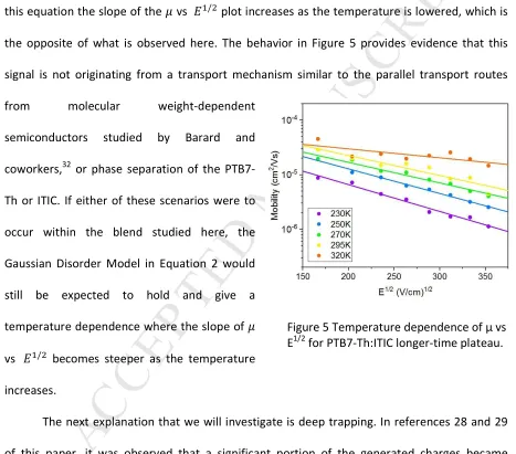
Prior work on two-plateau transients in organic semiconductors has shown that this phenomenon could be caused by deep trapping,28,29 ionic transport,30,31 or other parallel transport routes stemming from molecular weight variation or phase separation.32 We consider ionic transport unlikely because photogenerated ITIC⁻ ions are very large, making it improbable that they would drift through the film. To investigate the origin of these two transient plateaus, the plateaus are highlighted in Figure 4(a) and the electric field dependence taken from the early and time plateaus is shown in Figure 4(b). In this Figure it can be seen that the late-time plateau exhibits a strong negative field dependence, which is due to the late-time of the plateau becoming later with increasing electric field. Temperature dependence of the mobility for the late-time plateau was captured and is presented in Figure 5. At a given field it can be seen that the mobility increases as the temperature increases. We also observe in Figure 5 and
(a) (b)
[image:16.595.72.524.114.317.2]M
AN
US
CR
IP
T
AC
CE
PT
ED
15
in Supplementary Table S 1, that the slope of the mobility versus electric field becomes shallower with increasing temperature. However, in the Gaussian Disorder Model:
, , Σ exp &− '2 3* + , exp - / &' * + − Σ ,. (2)
where this equation is an extension of Equation 1, and , Σ, and E have the same definition.33 In
this equation the slope of the vs / plot increases as the temperature is lowered, which is the opposite of what is observed here. The behavior in Figure 5 provides evidence that this signal is not originating from a transport mechanism similar to the parallel transport routes from molecular weight-dependent
semiconductors studied by Barard and coworkers,32 or phase separation of the PTB7-Th or ITIC. If either of these scenarios were to occur within the blend studied here, the Gaussian Disorder Model in Equation 2 would still be expected to hold and give a temperature dependence where the slope of vs / becomes steeper as the temperature increases.
The next explanation that we will investigate is deep trapping. In references 28 and 29 of this paper, it was observed that a significant portion of the generated charges became trapped in deep trap states and lowered the current in the device. The remaining charges moved past the occupied deep states and reached the opposite electrode to form the
[image:17.595.66.533.235.646.2]M
AN
US
CR
IP
T
AC
CE
PT
ED
16
time current decay. A later-time plateau was then formed once the charges in the deep traps were slowly able to reactivate and reach the far electrode, occuring on the scale of 0.1 ms to 10 s.28 In agreement with these studies, we suggest that the late-time (~1 ms) plateau we observe in the PTB7-Th:ITIC transient is caused by charges reactivated from deep traps, and the earlier plateau (~100 µs) is due to untrapped charges.
We believe that the field and temperature dependence of this late-time plateau could provide a qualitative argument for the transport behavior of charges reactivated from deep traps. At low temperature, the Boltzmann factor in the hopping rate from site-to-site is
reduced, as determined by /01 / exp −2201⁄ exp − 43 1− 40 / when 41 > 40.27 In
this equation /01 is the hopping rate from site i to j, 201 is the site separation, and 40,1 is the
energy level of the site. This reduction of /01 at low temperature means that the charge will not
be able to hop forward out of the trap, but will need to find a closer energy level to jump to in a direction not aligned with the applied field. Movement in such a manner will lead to a negative dependence of vs / . At higher temperature the deeply trapped charges will gain thermal energy, lowering the activation energy needed to escape the trap and increasing the hopping rate, leading to a weaker field dependence of the mobility.
M
AN
US
CR
IP
T
AC
CE
PT
ED
17
5. Conclusions
Here we have reported the electron mobility of the new non-fullerene acceptors ITIC and IDTBR using the time of flight method. Pure ITIC films exhibited the highest electron mobility, with a zero-field value of 7.4 x 10⁻⁴ cm2/Vs. When put into a blend with the common donors PTB7-Th or P3HT, this mobility was lowered to a zero-field mobility of 1 x 10⁻⁴ cm2/Vs in both blends. The P3HT:IDTBR blend had the lowest electron mobility, with a zero-field value of 5.6 x 10⁻⁵ cm2/Vs. The P3HT:ITIC and P3HT:IDTBR films exhibit balanced hole and electron transport, allowing for high-performance OPVs to be made using these active layers. This balance is not as even in the PTB7-Th:ITIC blend, but this did have the highest electron mobility reported here and still shows promise for OPV application. Our results give new insight into charge mobilites of non-fullerene acceptors and suggest further enhancement of their electron mobility would lead to improvements in OPVs.
Acknowledgments: Natalie A. Mica and Stuart A. J. Thompson acknowledge student funding from EPSRC. [grant nos. EP/L015110/1 and EP/G03673X/1] Ifor D. W. Samuel acknowledges support from a Royal Society Wolfson Research Merit award.
M
AN
US
CR
IP
T
AC
CE
PT
ED
18
References
(1) Hummelen, J. C.; Knight, B. W.; Lepeq, F.; Wudl, F.; Yao, J.; Wilkins, C. L. Preparation and Characterization of Fulleroid and Methanofullerene Derivatives. J. Org. Chem. 1995,
60 (3), 532–538 DOI: 10.1021/jo00108a012.
(2) Yu, G.; Gao, J.; Hummelen, J. C.; Wudl, F.; Heeger, A. J. Polymer Photovoltaic Cells: Enhanced Efficiencies via a Network of Internal Donor-Acceptor Heterojunctions. Science
(80-. ). 1995, 270, 1789 DOI: 10.1126/science.270.5243.1789.
(3) Yan, J.; Saunders, B. R. Third-Generation Solar Cells: A Review and Comparison of Polymer:Fullerene, Hybrid Polymer and Perovskite Solar Cells. RSC Adv. 2014, 4 (82), 43286–43314 DOI: 10.1039/C4RA07064J.
(4) Brabec, C. J.; Gowrisanker, S.; Halls, J. J. M.; Laird, D.; Jia, S.; Williams, S. P. Polymer-Fullerene Bulk-Heterojunction Solar Cells. Adv. Mater. 2010, 22 (34), 3839–3856 DOI: 10.1002/adma.200903697.
(5) Lin, Y.; Wang, J.; Zhang, Z.-G.; Bai, H.; Li, Y.; Zhu, D.; Zhan, X. An Electron Acceptor Challenging Fullerenes for Efficient Polymer Solar Cells. Adv. Mater. 2015, 27 (7), 1170– 1174 DOI: 10.1002/adma.201404317.
(6) Holliday, S.; Ashraf, R. S.; Wadsworth, A.; Baran, D.; Yousaf, S. A.; Nielsen, C. B.; Tan, C.; Dimitrov, S. D.; Shang, Z.; Gasparini, N.; Brabec, C. J.; Salleo, A.; Durrant, J. R.; Mcculloch, I.; Alamoudi, M. High-Efficiency and Air-Stable P3HT-Based Polymer Solar Cells with a New Non-Fullerene Acceptor. Nat. Commun. 2016, 1–11 DOI:
10.1038/ncomms11585.
M
AN
US
CR
IP
T
AC
CE
PT
ED
19
Polymer Solar Cells. Adv. Mater. 2016, No. 28, 9423–9429 DOI: 10.1002/adma.201602776.
(8) Chu, C. W.; Shrotriya, V.; Li, G.; Yang, Y. Tuning Acceptor Energy Level for Efficient Charge Collection in Copper-Phthalocyanine-Based Organic Solar Cells. Appl. Phys. Lett.
2006, 88 (15), 153504 DOI: 10.1063/1.2194207.
(9) Proctor, C. M.; Kuik, M.; Nguyen, T.-Q. Charge Carrier Recombination in Organic Solar Cells. Prog. Polym. Sci. 2013, 38 (12), 1941–1960 DOI:
10.1016/j.progpolymsci.2013.08.008.
(10) Li, Z.; Xu, X.; Zhang, W.; Meng, X.; Ma, W.; Yartsev, A.; Inganäs, O.; Andersson, M. R.; Janssen, R. A. J.; Wang, E. High Performance All-Polymer Solar Cells by Synergistic Effects of Fine-Tuned Crystallinity and Solvent Annealing. J. Am. Chem. Soc. 2016, 138 (34), 10935–10944 DOI: 10.1021/jacs.6b04822.
(11) Kepler, R. G. Charge Carrier Production and Mobility in Anthracene Crystals. Phys. Rev.
1960, 119 (4), 1226–1229 DOI: 10.1103/PhysRev.119.1226.
(12) Pathipati, S. R.; Pavlica, E.; Treossi, E.; Rizzoli, R.; Veronese, G. P.; Palermo, V.; Chen, L.; Beljonne, D.; Cai, J.; Fasel, R.; Ruffieux, P.; Bratina, G. Modulation of Charge Transport Properties of Reduced Graphene Oxide by Submonolayer Physisorption of an Organic Dye. Org. Electron. physics, Mater. Appl. 2013, 14 (7), 1787–1792 DOI: 10.1016/j.orgel.2013.03.005.
(13) Kokil, A.; Yang, K.; Kumar, J. Techniques for Characterization of Charge Carrier Mobility in Organic Semiconductors. J. Polym. Sci. Part B Polym. Phys. 2012, 50 (15), 1130–1144 DOI: 10.1002/polb.23103.
M
AN
US
CR
IP
T
AC
CE
PT
ED
20
Y.-Z.; Su, T.-H.; Huang, B.-Y.; Chang, W.-C.; Liu, Y.-H. Downscaling the Sample Thickness to Sub-Micrometers by Employing Organic Photovoltaic Materials as a Charge-Generation Layer in the Time-of-Flight Measurement. Sci. Rep. 2015, 5 (April), 10384 DOI: 10.1038/srep10384.
(15) Gambino, S.; Bansal, A. K.; Samuel, I. D. W. Comparison of Hole Mobility in Thick and Thin Films of a Conjugated Polymer. Org. Electron. physics, Mater. Appl. 2010, 11 (3), 467–471 DOI: 10.1016/j.orgel.2009.11.030.
(16) Campbell, A. J.; Bradley, D. D. C.; Antoniadis, H. Dispersive Electron Transport in an Electroluminescent Polyfluorene Copolymer Measured by the Current Integration Time-of-Flight Method. Appl. Phys. Lett. 2001, 79 (14), 2133–2135 DOI: 10.1063/1.1406143. (17) Frost, J. M.; Cheynis, F.; Tuladhar, S. M.; Nelson, J. Influence of Polymer-Blend
Morphology on Charge Transport and Photocurrent Generation in Donor − Acceptor Polymer Blends. Nano Lett. 2006, 6 (8), 1674–1681 DOI: 10.1021/nl0608386.
(18) Pavlica, E.; Penumala, R. B.; Bratina, G. The Role of Local Potential Minima on Charge Transport in Thin Organic Semiconductor Layers. Org. Electron. 2017, 42, 221–227 DOI: 10.1016/j.orgel.2016.12.038.
(19) Tong, K. L.; Tsang, S. W.; Tsung, K. K.; Tse, S. C.; So, S. K. Hole Transport in Molecularly Doped Naphthyl Diamine. J. Appl. Phys. 2007, 102 (9) DOI: 10.1063/1.2804109.
(20) Lampbert, M.; Mark, P. Current Injection in Solids, 1st ed.; Booker, H., DeClaris, N., Eds.; Academic Press Inc., 1970.
M
AN
US
CR
IP
T
AC
CE
PT
ED
21
Phys. Lett. 2008, 93 (10), 252104–123509 DOI: 10.1063/1.3055608͔.
(22) McNeill, C. R.; Greenham, N. C. Charge Transport Dynamics of Polymer Solar Cells under Operating Conditions: Influence of Trap Filling. Appl. Phys. Lett. 2008, 93 (20), 1– 4 DOI: 10.1063/1.3033372.
(23) Choulis, S. A.; Kim, Y.; Nelson, J.; Bradley, D. D. C.; Giles, M.; Shkunov, M.;
Mcculloch, I. High Ambipolar and Balanced Carrier Mobility in Regioregular Poly ( 3-Hexylthiophene ). Appl. Phys. Lett. 2015, 3890 (2004), 1 DOI: 10.1063/1.1805175. (24) Ebenhoch, B.; Thomson, S. A. J.; Genevi??ius, K.; Ju??ka, G.; Samuel, I. D. W. Charge
Carrier Mobility of the Organic Photovoltaic Materials PTB7 and PC71BM and Its Influence on Device Performance. Org. Electron. physics, Mater. Appl. 2015, 22, 62–68 DOI: 10.1016/j.orgel.2015.03.013.
(25) Reyes-Reyes, M.; Kim, K.; Carroll, D. L. High-Efficiency Photovoltaic Devices Based on Annealed Poly(3-Hexylthiophene) and 1-(3-Methoxycarbonyl)-Propyl-1- Phenyl- (6,6) C61 Blends. Appl. Phys. Lett. 2005, 87 (8) DOI: 10.1063/1.2006986.
(26) Lu, L.; Chen, W.; Xu, T.; Yu, L. High-Performance Ternary Blend Polymer Solar Cells Involving Both Energy Transfer and Hole Relay Processes. Nat. Commun. 2015, 6, 7327 DOI: 10.1038/ncomms8327.
(27) Miller, A.; Abrahams, E. Impurity Conduction at Low Concentrations. Phys. Rev. 1960,
120 (3), 745–755.
(28) Li, C.; Duan, L.; Li, H.; Qiu, Y. Universal Trap Effect in Carrier Transport of Disordered Organic Semiconductors: Transition from Shallow Trapping to Deep Trapping. J. Phys.
Chem. C 2014, 118 (20), 10651–10660 DOI: 10.1021/jp5022906.
M
AN
US
CR
IP
T
AC
CE
PT
ED
22
Energetic Trap States in Organic Photovoltaic Devices. Adv. Energy Mater. 2012, 2 (1), 111–119 DOI: 10.1002/aenm.201100541.
(30) Iino, H.; Hanna, J. I.; Haarer, D. Electronic and Ionic Carrier Transport in Discotic Liquid Crystalline Photoconductor. Phys. Rev. B - Condens. Matter Mater. Phys. 2005, 72 (19), 1–4 DOI: 10.1103/PhysRevB.72.193203.
(31) Funahashi, M.; Hanna, J. I. Impurity Effect on Charge Carrier Transport in Smectic Liquid Crystals. Chem. Phys. Lett. 2004, 397 (4–6), 319–323 DOI: 10.1016/j.cplett.2004.08.125. (32) Barard, S.; Heeney, M.; Chen, L.; Cölle, M.; Shkunov, M.; Mcculloch, I.; Stingelin, N.;
Philips, M.; Kreouzis, T. Separate Charge Transport Pathways Determined by the Time of Flight Method in Bimodal Polytriarylamine. J. Appl. Phys. 2009, 105 (1) DOI:
10.1063/1.3054180.
(33) Bässler, H. Charge Transport in Disordered Organic Photoconductors a Monte Carlo Simulation Study. Phys. status solidi 1993, 175 (1), 15–56 DOI:
M
AN
US
CR
IP
T
AC
CE
PT
ED
Time of Flight Method
Natalie A. Mica, Stuart A. J. Thomson, Ifor D. W. Samuel
Organic Semiconductor Centre, SUPA, School of Physics and Astronomy, University of St
Andrews, St Andrews, KY16 9SS, UK
Highlights:
• Electron transients were observed in ITIC and IDTBR films
• The electron mobility is comparable to the hole mobility in some blends