Available Online At www.ijpret.com
INTERNATIONAL JOURNAL OF PURE AND
APPLIED RESEARCH IN ENGINEERING AND
TECHNOLOGY
A PATH FOR HORIZING YOUR INNOVATIVE WORKVLSI IMPLEMENTATION OF 8, 16 AND 32 BIT MAXIMUM LENGTH LFSR FOR
CRYPTOGRAGHY APPLICATIONS
TARANNUM U. PATHAN, DR. P. K. DAKHOLE
1. M. Tech 3rd sem (Electronics Engineering), Yeshwantrao Chavan College of Engineering, Nagpur (M.S.), India.
2. Department of Electronics Engineering, Yeshwantrao Chavan College of Engineering, Nagpur (M.S.), India.
Accepted Date:
27/02/2013
Publish Date:
01/04/2013
Keywords
LFSR,
FPGA,
PRNSG,
VERILOG
Corresponding Author Ms. Tarannums U. Pathan
Abstract
LFSR based PN sequence generator technique is an important tool in
cryptography. They are used to generate secret keys, to encrypt messages
or to mask the content of certain protocol by combining the content with
random sequence. The main purpose of this paper is to study the FPGA
implementation of 8, 16 and 32 bit maximum length LFSR pseudo random
number generator system which is a parameterized module by using
Verilog HDL and its performance analysis. We have used FPGA to explain
how FPGA’s ease the hardware implementation part of cryptography
systems. The analysis is conceded out to find area, speed and power
requirement in FPGA as the size of LFSR is increased. The comparative
study of 8, 16 and 32 bit LFSR on FPGA is shown here to understand the
on chip verification. The greatest advantage of FPGA is that it is a
predesigned reconfigurable IC. In this paper we have used XOR gate for
taping. Also we can use XNOR gate for taping. In this paper, we also
Available Online At www.ijpret.com
I. INTRODUCTION
Today cryptography is an integral part of our
lives. The list of public applications is long, and
many spring from the use of internet. This global
communication system has provided us not only
with new buzz words such as “24/7 shopping”,
“one-click-buy” and “JIT-services” but also with a
new and convenient ways of performing tasks.In
addition, confidentiality of communication, many
new tasks like data integrity, message
authentication, or non-repudiation have been
added [1][3]. Pseudorandom number generators
(PRNGs) are used in modern cryptography to
transform a small initial value into a long
sequence of seemingly random bits[2][3].There
arevarious methods for generating
pseudo-random numbers are known [6][7][10].Most of
them are based, on linear congruential equations,
which require a number of time consuming
arithmetic operations, the hardware
implementation is very complicated and the
safety performance is poor to be used in
cryptography[6][7]. Most of them are based on
Blum BlumShub (BBS) method for generating PN
sequence as it is non periodic cryptographically
secure method .But performance is poor as the
time required is more and memory utilization is
more in BBS as no. of flip-flops required are
more[10].In contrast, many designs for PRNGs
are based on linear feedback shift registers
(LFSRs), which can be constructed in such a way
as to have optimal statistical and periodical
properties and permits very fast generation of
binary PN sequences[9]. In this paper, we have
implemented 8, 16 and 32 bit maximum length
LFSR which can give the maximum states of PN
sequence. Also we have presented the
comparison of performance analysis of 8, 16,32
bit LFSR’s based on synthesis and simulation
result on FPGA using verilog hardware descriptive
language(HDL) with maximum length feedback
polynomial to understand the area, speed and
power requirement[11]. The target device we
have used is Xilinx Virtex6 XA9572XL FPGA with
target technology Automotive 9500XL and
performed simulation and synthesis using Xilinx
ISE 13.1.
FPGA is a predesigned reconfigurable IC. It has
the ability to reconfigure its circuitry for a desired
application or function at any time after
manufacturing. It is an adaptive hardware that
continuously changes in response to the input
data or processing environmentThe FPGA
configuration is generally defined using a
hardware description language (HDL), similar to
Available Online At www.ijpret.com circuit (ASIC).FPGAs can be used to implement
any logical function that an ASIC can perform.
Because of various advantages and rapid
prototype development can possible, so FPGA is
chosen.
II.LINEARFEEDBACKSHIFTREGISTER(LFSR)
LFSR is a shift register that, when clocked,
advances the signal through the register from
one bit to the next most-significant bit as shown
in the Fig.1[8]-[11]. Some of the outputs are
combined in exclusive-OR configuration to form a
feedback mechanism as shown in Fig.1. A linear
feedback shift register can be formed by
performing exclusive-OR on the outputs of two or
more of the flip-flops together and feeding those
outputs back into the input of one of the
flip-flops as shown. Linear feedback shift registers
make extremely good pseudorandom pattern
generators. When the outputs of the flip-flops
are loaded with a seed value (anything except all
0s, which would cause the LFSR to locked at all 0
patterns) and when the LFSR is clocked, it will
generate a PN sequence of 1s and 0s[8]-[11]. The
only signal necessary to generate it is clock.
Applications of LFSRs include generating
pseudo-random numbers, pseudo-noise sequences, fast
digital counters, and whitening sequences.
Figure1.Basic module of 4-bit LFSR[9]
A. Implementation of basic module of 4-bit LFSR
Fig.1 shows the basic block diagram of 4-bit
LFSR PN sequence is generated in Verilog
according to the following circuit based on the
concept of shift register. In the Fig.1, X1, X2, X3
and X4 are the D flip-flops. The bits in the LFSR
state which influence the input are called taps. A
maximum-length LFSR produces an m-sequence
(i.e. it cycles through all possible (2n– 1) states
within the shift register except the state where all
bits are zero), unless it contains all zeros, in which
case it will never change. The sequence of
numbers generated by this method is random.
The period of the sequence is (2n - 1), where n is
the number of shift registers used in the design
[8]-[11].
For 32 bit LFSR, the states are 4294967296 .This
is large enough for most of the practical
Available Online At www.ijpret.com taps for feedback in an LFSR can be expressed in
finite field arithmetic as a polynomial mod 2. This
means that the coefficients of the polynomial
must be 1's or 0's. This is called the feedback
polynomial or characteristic polynomial. For
example, if the taps are at the 16th, 15th, 13th
and 4th bits (as shown),
The feedback polynomial is X16 + X15 + X13 + X4 +
1.
B. Rules for Selecting the Maximum length
feedback or Characteristics Polynomial
The '1’ in the polynomial does not correspond to
a tap it corresponds to the input to the first bit
(i.e. x0which is equivalent to 1).The powers of the
terms represent the tapped bits, counting from
the left[9]. The first and last bits are always
connected as an input and output tap
respectively. The LFSR will only be
maximum-length if the number of taps is even;
just 2 or 4 taps can suffice even for extremely
long sequences[9]. The set of taps taken all
together, not pair wise must be relatively prime.
In other words, there must be no common divisor
to all taps. Once one maximum-length tap
sequence has been found, another automatically
follows [9]. If the tap sequence, in an n-bit LFSR,
is [n, A, B, C, 0], where the 0 corresponds to the
x0 = 1 term, then the corresponding 'mirror'
sequence is [n, n − C, n − B, n − A, 0]. So the tap
sequence [32, 7, 3, 2, 0] has as its counterpart
[32, 30, 29, 25, 0][9]. Both gives a
maximum-length sequence.
TABLE I
TAPS FOR MAXIMUM-LENGTH LFSR[11]
N XOR from Maximum Length Feedback
polynomial
4-bits 4,3 X4+ X3+1
8-bits 8,6,5,4 X8+X6+X5+X4+1
16-bits 16,15,13,4 X16+X15+X13+X4+1
32-bits 32,22,2,1 X32+X22+X2+X1+1
Table I shows the tapping conditions for 4, 8,
16,32 and 64 bits LFSRs and the corresponding
maximum length feedback or characteristics
polynomial.
III. SYNTHESISANDSIMULATION
In this design, we describe the RTL-level of the
LFSR pseudo-random number generator for 8-bit,
16- bit and 32- bit using Verilog language, and use
the Xilinx Virtex6 XC6VCX75T device as the target
chip. Then we synthesize, place and route on the
Xilinx ISE 13.1 platform. Finally we use ISE
Available Online At www.ijpret.com A. Timing Simulation
The simulation waveform for 8-bit, 16-bit and
32-bit are shown in Fig.3, Fig.4 and Fig.5 respectively
with mininum clock period of 29.7 ns.
B. Design & Simulation of 8-Bit LFSR
Figure2 shows 8-bit LFSR with maximum length
feedback polynomial X8 + X6 + X5 + X4 + 1
generates 28= 255 random states, which is
verified from the simulation waveform under the
maximum clock frequency 33.670 MHz. The
circuit diagram for 8-bit LFSR with maximum
length polynomial is shown in Fig. 2. The timing
simulation is shown in Fig. 3 from 20 ns and after
255 states the random output is repeating again.
Figure2. Block Diagram of 8- Bit LFSR with
maximum length Feedback Polynomial X8 + X6 +
X5 + X4 + 1
C. Design & Simulation of 16-Bit LFSR
16-bit LFSR with maximum length feedback
polynomial X16 + X14 + X13 + X11 + 1 generates 216
-1 = 65535 random outputs, which is verified from
the simulation waveform under the maximum
clock frequency 33.670 MHz.The circuit diagram
for 16-bit LFSR with maximum length polynomial
is shown in Fig. 3. The timing simulation is shown
in Fig.6 from 20 ns. It shows after 65535 states
the sequence starts repeating again.
Figure3. Block Diagram of 16- Bit LFSR with
maximum length
Feedback Polynomial X16 + X14 + X13 + X11 + 1
D. Design & Simulation of 32-Bit LFSR
32-bit LFSR with maximum length feedback
polynomial X32 + X22 + X2 + X1 + 1 for which 232 -1
= 429, 49,67,295 random outputs, which is
verified from the simulation waveform under the
maximum clock frequency 33.670 MHz. The
circuit diagram for 32-bit LFSR with maximum
Available Online At www.ijpret.com simulation is shown in Fig. 7 starting from 20 ns
and we can observe here the simulation is
running for a long time to complete the
sequence.
Figure 4. Block Diagram of 32- Bit LFSR for
maximum length Feedback
Polynomial X32 + X22 + X2 + X1 + 1
E. Synthesis Result and comparison between 8,
16, 32 bit,. The synthesis and simulation report
for 8, 16 and 32 bit LFSR by using maximum
length feedback polynomial are given in Table 2.
From the table we can find the total memory
usage of different length LFSR.
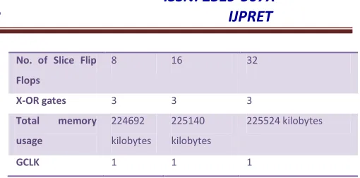
TABLE IISIMULATION AND SYNTHESIS RESULT
Performance 8 Bit 16 Bit 32 Bit
Total no. of
Random
states generated
255 65535 4,29,49,67,295
Min Clock Period 29.7ns 29.7ns 29.7ns
Shift registers 8 16 32
No. of Slice Flip
Flops
8 16 32
X-OR gates 3 3 3
Total memory
usage
224692 kilobytes
225140 kilobytes
225524 kilobytes
GCLK 1 1 1
IV. CONCLUSION
It is clearly found from the synthesis and
simulation result that 8 bit, 16 bit and 32 bit LFSR
with maximum feedback polynomial can
generate maximum random output. Also we can
find the memory utilization is approximately
same for all three LFSR. Hardware requirement in
8-bit LFSR is less as compared to 32 bit LFSR. The
area is more in 32-bit LFSR but it generates
maximum PN sequences. Definitely 32 bit LFSR
with maximum length feedback polynomial will
generate large sequence which is more secure for
the cryptography applications. In the practical
use 8-bit and 16-bit LFSR is sufficient for different
cryptographic applications.
References
1. M. Luby, Pseudorandomness and
Cryptographic Applications, Princeton University
Press, 1996.
2. Ding Jun, Li Na, GuoYixiong, “A high-
performance pseudo random number
Available Online At www.ijpret.com Conference on Wireless Networks and
Information Systems.
3. Jiang Hao, Li Zheying, “On the Production of
Pseudo- random Numbers in Cryptography” in
Journal Changzhou Teacher College of
Technology, Vo1. 7, No. 4, Dec. 2001.
4. F. James, “A Review of Pseudo-random
Number Generators,”Computer Physics
Communications 60, 1990.
5. Katti, R.S. Srinivasan, S.K., “Efficient hardware
implementation of a new pseudo-random bit
sequence generator” IEEE International
Symposium on Circuits and Systems, 2009
6. C. Li and B. Sun, “Using linear congruential
generators for cryptographic purposes”, In
Proceedings of the ISCA 20th International
Conference on Computers and Their
Applications, pp.13-18, March 2005.
7. L'Ecuyer, Pierre, “Tables of Linear
Congruential Generators of Different Sizes and
Good Lattice Structure,” Mathematics of
Computation, Vol. 68, No. 225, 1999, Pages
249-260.
8. Goresky, M. and Klapper, A.M. Fibonacci and
Galois Representations of feedback-with-carry
shift registers, IEEE Transactions onInformation
Theory, Nov 2002,Volume:48, On page(s): 2826 –
2836.
9. Panda Amit K, Rajput P, Shukla B, “Design of
Multi Bit LFSR PNRG and Performance
comparison on FPGA using VHDL”, International
Journal of Advances in Engineering & Technology
(IJAET), Mar 2012, Vol. 3, Issue 1, pp. 566-571.
10. Sewak K, Rajput P, Panda Amit K, “FPGA
Implementation o 16 bit BBS and LFSR PN
Sequence Generator: A Comparative Study”, In
Proce. Of the IEEE Student Conference on
Electrical, Electronics and Computer Sciences
2012, 1-2 Mar 2012, NIT Bhopal, India.
11. Efficient Shift Registers, LFSR Counters, and
Available Online At www.ijpret.com
Figure. 5 Timing Simulation waveform of 8-Bit LFSR : Total 255 periods
Figure6. Timing Simulation waveform of 16-Bit LFSR: Total Total 65535 periods
Figure7. Timing Simulation waveform of