Abstract—The performance of the S-Box represents an important factor in the overall performance of the AES cryptography systems. It affects the speed, area, and the power consumption of the AES. In attempts to improve the performance of the S-box byte substitution a number of techniques were presented in the literature. In this paper, we classify the S-box byte substitution optimization techniques as those based on hardware, software, and combined hardware/software. We then move on to propose a new highly parallel and area-efficient S-box architecture for AES byte substitution. We also conduct a performance analysis and comparison of the proposed architecture with those achieved by existing techniques. The comparison shows that the proposed architecture outperforms the existing techniques in terms of speed and area.
Index Terms—Cryptography, advanced encryption standard (AES), s-box byte substitution, parallel s-box architecture, efficient s-box.
I. INTRODUCTION
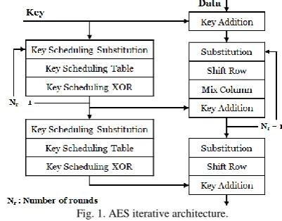
According to the AES data to be encrypted is divided into equally sized blocks each is called a state. The algorithm performs a series of mathematical operations on each state based on the Substitution-Permutation Network principle to produce the cipher text. The algorithm starts with an initial step to add the round key to the state. After that, the state enters the main loop which includes four repeated operations:
sub bytes, shift rows, mix columns, and add round key. This is followed by a final iteration that excludes mix columns. There have been a number of improvements to enhance efficiency of the original AES in terms of area, delay, and power consumption [2]-[4]. Fig. 1 provides a simple illustration of the AES encryption process.
Among the four loop operations, the substitution of bytes is performed in what is known as the substitution box (S-Box). The S-Box performs a non-linear transformation on data by
Manuscript received October 13, 2013; revised January 23, 2014. This
work was supported in part by Kuwait University under Grant WI04/10. The authors are with the Department of Information Science, College of Computing Sciences and Engineering (CCSE), Kuwait University, Kuwait (e-mail: [email protected], [email protected]).
replacing each individual byte by a different byte. The main purpose of the byte substitution is to bring confusion to the data to be encrypted using the AES [5]. The replacement bytes can be obtained on the fly by determining the multiplicative inverse of a given state in finite field GF (256) followed by affine transformation in GF 2). Alternatively, the replacement bytes can be pre-calculated and stored in a look-up table (LUT) in the S-Box. It should be noted that the replacement bytes for encryption are different than the ones used for decryption.
Fig. 1. AES iterative architecture.
Byte substitution is considered one of the most complex loop operations. Hence, a number of research efforts were devoted to the optimization of the byte substitution both in time, hardware complexity, and power consumption [6]-[15]. The research work reported in this paper concentrates on proposing a new method for designing a highly parallel area-efficient S-Box architecture for the AES cryptosystem.
The paper is organized as follows. In Section II, we provide some background material. In Section III, we provide a brief summary of the existing S-Box realization techniques. In Section IV, we preview the related work reported in the literature. In Section V, we introduce the proposed S-Box architecture and algorithm. In Section VI, we illustrate the CMOS implementation of the proposed architecture. In Section VII, we provide estimation of the delay and area needed for the proposed architecture. In Section VIII, we provide a comparison with existing techniques. Section VIX provides a number of concluding remarks.
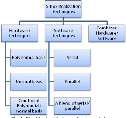
II.EXISTING S-BOX REALIZATION TECHNIQUES
Fig. 2 illustrates our classification of the S-Box byte substitution realization techniques.
A. Hardware Techniques
Hardware techniques are the ones that compute substitution
A Highly Parallel Area Efficient S-Box Architecture for
AES Byte-Substitution
Mostafa Abd-El-Barr and Altaf Al-Farhan
values rather than reading them from a memory. The representation of the finite field elements has an impact on the hardware in terms of gates count and chip area. Polynomial and normal bases are the two popular representations. The most compact implementation known is the one proposed by Canright [9] in normal bases, which used sub-field arithmetic to compute AES S-Box. Canright has examined all possible choices of representations in each sub-field including purely polynomial, purely normal basis, and a combination of both. The total number of isomorphisms was found to be 432 different choices. The case that uses polynomial basis for all sub-fields is the one proposed by Satoh et al., [7]. The optimal representation, which has the minimum gate count, was obtained using an exhaustive tree-search algorithm. In each sub-field both inverse and multiplication operations are required. These mathematical operations were discussed in details for the most compact case. Further optimization was done by calculating a merged S-Box for both encryption and decryption. The merged S-Box is 20% more compact than separate computations of S-Box and its inverse. Canright's implementation is best suited for limited space applications, e.g. mobile applications. The technique can also be parallelized and pipelined for high throughput applications. The main drawback of this implementation is its relatively long critical path and high power consumption [10]. Alternatively, Nikova et al., [11] proposed an implementation using normal bases that differs in the level of decomposition. Both normal bases implementations [9] and [11] are compact, however the choice of which to use depends on the application and hardware technology. The polynomial representations by Satoh et al., [7], Rijmen [12], and Wolkerstorfer et al., [13] were less efficient compared to normal bases representations in terms of chip area.
The implementation that resulted in least power consumption according to [10] is the one proposed by Bertoni
et al., [14]. The proposed solution uses a synthesis methodology composed of three main blocks: a multi-level decoder followed by a permutation block, which does the S-Box computation, and finally an encoder.
Fig. 2. Classification of s-box realization techniques.
B. Software Techniques
Software implementation is based on using a look up table (LUT). In this case a RAM is used to store pre-calculated
S-Box values. Techniques that are included under such approach vary from the totally serial (slow) to the totally parallel (fast) ones. In the totally serial approach each byte of the State is substituted by the corresponding S-Box byte one at a time in a serial manner. Consider, for example, the 128 bit AES case. In this case each of the 16 State bytes is replaced by the corresponding S-Box byte. Assume that the area required for the LUT is A, and the time needed to substitute one byte is
T, then the total time needed to substitute all sixteen State bytes is 16T. The other extreme is the totally parallel approach. In this case there are 16 S-Boxes each consists of 16 bytes such that all of the 16 bytes of the State are substituted by their respective corresponding S-Box bytes simultaneously. The total time needed to substitute all sixteen State bytes is T, while the area required is 16A.
The two extreme cases: the most restricted serial and the most flexible parallel ones are illustrated in Fig. 3. In between, there exist a number of possible intermediate cases. These intermediate cases exhibit tradeoffs between area and throughput.
C. Hardware/Software Techniques
In this case use is made of pipelining (hardware technique) in building the S-box employing small substitution tables constructed using LUTs (software technique) [15]. The basic idea of the approach is that the original large truth-table of say 8-varaible function is broken down into a set of smaller size multiplexer-switched truth-table of say 4-variable functions using the Shannon expansion. The smaller tables were then mapped into 4-LUT of Xilinx FPGA. The approach shows significant improvement in the overall throughput.
III. RELATED WORK
The traditional basic lookup table implementations (hw-lut) are relatively fast and can achieve better performance with some modifications [10]. One way to reduce power consumption is to divide the 256 bytes S-Box into smaller tables with the aim being to reduce the switching activities. The use of smaller LUTs of different sizes ranging from 16 to 128 bytes was examined in [10]. However, only the result for the 16 bytes size was reported (sub16-lut). The solution proposed in [8] not only uses small LUTs, but also reduces execution time at the expense of doubling the chip area required.
The main drawback of the approach in [8] is the possibility of conflict in accessing a given table. In this case, the author suggested using a busy bit with each table such that if the busy bit is ON, then it means that the table is currently in use and cannot be accessed in the current cycle. This will lead to a slowdown in the rate at which the S-Box substitution is performed. In the next Section, we propose an S-Box architecture which overcomes the conflict problem in addition to achieving higher throughput.
(a)Totally serial s-box architecture.
(b)Totally parallel s-box architecture Fig. 3. Serial versus parallel s-box architecture.
IV. PROPOSED S-BOX ARCHITECTURE
The basic idea of the proposed scheme is to perform byte substitution of an AES state using a number of 2×2 tables that are organized in groups. Each group has 16 small s-boxes of size 2×2 organized in a bigger table of four rows and four columns. The small tables are selected based on row and column values. The size of each group is 64 bytes, which is one fourth the regular S-box size (Refer to Fig. 4). Each byte needs a minimum of four groups to cover all values of the original S-box. More groups that are multiples of four can be used to achieve parallelism. If we consider the use of 16 groups, then 16 bytes can be processed simultaneously.
The advantage of using groups of small tables is two-fold. On one hand it simplifies table indexing and on the other hand it leads to reduced power consumption. These are achieved at the expense of size (area) increase 4 times the original S-box size.
The required algorithm for byte substitution is as follows:
For each byte in a state do:
V.PROPOSED S-BOX CMOSIMPLEMENTATION
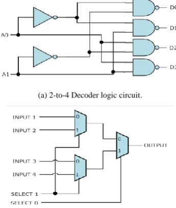
In order to choose one group out of four, a 2-to-4 decoder is used. Two more 2-to-4 decoders are required to choose the row and column within the selected group. We choose to use NAND decoders to comply with CMOS technology. The decoder circuit is shown in Fig. 5(a). Once decoding is done, the LUT to be used is known. The two right most bits of the byte processed are used as an index to the 2×2 LUT. These two bits are connected to the select lines of a 4-to-1 multiplexer having the table data as inputs and the S-Box substitution value as the output. All the 4-to-1 multiplexers implemented are constructed by three 2-to-1 multiplexers for simplicity (Refer to Fig. 5(b)). The following is an illustration of three different ways to implement 2-to-1 multiplexers:
A. Gate-Level Implementation (NAND-NAND) CMOS Implementation
Each CMOS NAND gate consists of four transistors. Three NAND gates and an inverter can be used as shown in Fig. 5(c) to perform the operation of a 2-to1 MUX. For our 2×2 LUT we need a 4-to-1 MUX which can be constructed using three 2-to-1 MUX as shown in Fig. 5(b).
B. Gate-Level Implementation (NAND-NAND) CMOS Implementation
Pass transistor logic can be used as shown in Fig. 5(d) to implement a 2-to-1 multiplexer. The inverter added at the output to retain logic level. The 4-to-1 multiplexer needed for S-Box LUT is constructed using three 2-to-1 multiplexers.
C. Transmission Gates Implementation
Transmission gates are simply switches which can act as a two-to-one multiplexer as shown in Fig. 5(e). In this case the number of transistors required is less than the former implementations. Again, 4-to-1 multiplexers are constructed out of 2-to-1 ones.
VI. DELAY AND AREA ESTIMATION
All results reported in this paper are based on using 0.35 μm CMOS technology of AMS Corp. [16]. Since the decoding part for our three proposed solutions is the same, the associated delay and area are consequently identical. Remember that four bytes of a state are processed in parallel. This implies that 72 NAND gates are required, as every byte needs three 2-to-4 decoders. Each 2-to-4 decoders requires six NAND gates assuming that inverters in implemented using NAND gates. Area is measured using gate equivalents (GE), where one gate equivalent corresponds to one NAND2 gate. 1) Use the left-most two bits to select a group of four, 2) Use the next left-most bits to select a row within a group, 3) Use the next left-most bits to select a column—The selected column and the row identified in steps 2 above intersect at a point that identifies a specific 2×2 table, 4) Use the two right-most bits to lookup the table and obtain
According to the CMOS library used one NAND2 gate has 0.1 ns delay. Given that decoding of the row and column are done in parallel, the total decoding time is 1.6 ns for one AES state.
(a) The first four bytes of a given state are processed.
(b) Selecting a group.
(c) Identifying the row, the column, and the LUT containing the substitution value
Fig. 4. An illustrative example of the proposed S-Box architecture.
(a) 2-to-4 Decoder logic circuit.
(b) 4-to-1 MUX using three 2-to-1 MUX.
(c) NAND-based realization of 2-to-1 MUX.
(d) Pass transistor based realization of 2-to-1 MUX.
(e) Transmission gate based realization of 2-to-1 MUX.
Fig. 5. The CMOS gate-level realization.
For the first proposed implementation, three 2-to-1 multiplexers are needed for each byte. This means that we need twelve 2-to-1 multiplexers to process four bytes of a state, that is 48 GEs given that each 2-to-1 multiplexer is 4 GEs. The delay for multiplexing is four times the delay of one 4-to-1 multiplexer, that is 2.4 ns.
For the second proposed implementation, two pass transistors which construct a 2-to-1 multiplexer can be estimated to consume an area equivalent to ½ of a NAND2 area. We need an inverter for the selector which has a size of 1 GE. In addition to two cascaded inverters at the output to retain the logic value. The two inverters consume the area of 2 GEs. The sum is 3.5 GEs for each 2-to-1 multiplexer yielding a total of 42 GEs (12×3.5). The delay of one 2-to-1 multiplexer is the delay of the transistors plus the delay of the two inverters, that is 0.25 ns. Therefore, the total delay can be estimated as 2 ns (8×0.25).
In the third proposed implementation, each transmission gate consumes an area equivalent to ½ of a NAND2. The inverter for the selector consumes 1 GE. The sum is 2 GEs per 2-to-1 multiplexer. This gives a total area of 24 GEs (12×2). The critical path delay for the data of the 2-to-1 multiplexer is estimated as the delay of one two input NAND gate yielding a total of 0.8 ns (8×0.1). The delay and area estimations of the three possible implementations are summarized in Table I.
TABLEI:DELAY AND AREA ESTIMATION OF THE PROPOSED SOLUTIONS
Implementation
First Propose
d Solution (NAND)
Second Proposed
Solution (Pass Transistor)
Third Proposed
Solution (Transmission
Gate)
Decoders Delay (ns) 1.6 1.6 1.6
Multiplexers Delay (ns) 2.4 2 0.8
Total Delay (ns) 4 3.6 2.4
Decoders Area (GE) 72 72 72
Multiplexers Area (GE) 48 42 24
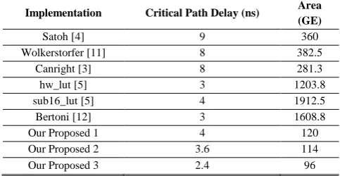
VII. COMPARISON
Based on the minimum values of area and delay obtained from [10], a comparison is made between various AES S-Box techniques (Refer to Table II).
TABLE II: DELAY AND AREA COMPARISONS
Implementation Critical Path Delay (ns) Area
(GE)
Satoh [4] 9 360
Wolkerstorfer [11] 8 382.5
Canright [3] 8 281.3
hw_lut [5] 3 1203.8
sub16_lut [5] 4 1912.5
Bertoni [12] 3 1608.8
Our Proposed 1 4 120
Our Proposed 2 3.6 114
Our Proposed 3 2.4 96
As can be seen from the table, when it comes to critical path delay, the third proposed implementation (using Transmission Gates) outperforms Bertoni's [12] and hw_lut [5] approaches by 20%. And when it comes to gate equivalent (GE) the third proposed implementation requires about one third the gate equivalent (GE) used by Canright's [3] compact implementation.
VIII. CONCLUSION
A highly parallel area efficient S-Box Architecture for AES Byte-Substitution is introduced in this paper. The proposed is modular, compact, and is efficient in terms of time and area. The design uses parallelism and can be pipelined to maximize throughput and reduce delay. The authors are currently exploring those objectives as future work.
ACKNOWLEDGMENT
The authors would like to acknowledge the financial support received from Kuwait University in the form of the funded research project WI 04/10.
REFERENCES
[1] J. Daemen and V. Rijmen, "AES proposal: rijndael," in Proc. First
Advanced Encryption Standard (AES) Conference, vol. 3, 1998.
[2] H. Samiee, R. E. Atani, and H. Amindavar, "A novel area-throughput optimized architecture for the AES algorithm," in Proc. International Conference on Electronic Devices, Systems and Applications
(ICEDSA), 2011, pp. 29-32.
[3] T. Rahman, S. Pan, and Q. Zhang, "Design of a High Throughput 128-bit AES (Rijndael Block Cipher)," in Proc. International Multi
Conference of Engineers and Computer Scientists, vol. 2, 2010.
[4] A. Hodjat, and I. Verbauwhede, "Area-throughput trade-offs for fully pipelined 30 to 70 Gbits/s AES processors,"IEEE Transactions on
Computers, vol. 55, no. 4, pp. 366-372, April 2006.
[5] C. E. Shannon, "Communication theory of secrecy systems," Bell
System Technical Journal, vol. 28, no. 4, pp. 656-715, 1949.
[6] D. Chen, G. Shou, Y. Hu, and Z. Guo, "Efficient architecture and implementations of AES," in Proc. Third International Conference on
Advanced Computer Theory and Engineering (ICACTE), 2010, vol. 6,
pp. 295-298.
[7] A. Satoh, S. Morioka, K. Takano, and S. Munetoh, "A compact rijndael hardware architecture with S-box optimization," in Advances in
Cryptology – ASIACRYPT, 2001, vol. 2248, pp. 239–254.
[8] H. Li, "A parallel S-box architecture for AES byte substitution," in
Proc. International Conference on Communications, Circuits and
Systems (ICCCAS),2004, vol. 1, pp. 1-3.
[9] D. Canright, "A very compact S-Box for AES," in Cryptographic
Hardware and Embedded Systems — CHES 2005, Springer Verlag, pp.
441–455, 2005.
[10] S. Tillich, M. Feldhofer, and J. Großschädl, "Area, delay, and power characteristics of standard-cell implementations of the AES S-box," in
Embedded Computer Systems: Architectures, Modeling, and
Simulation, Springer Verlag, pp. 457-466, 2006.
[11] S. Nikova, V. Rijmen, and M. Schlaffer, "Using Normal Bases for Compact Hardware Implementations of the AES S-Box," in Security
and Cryptography for Networks, Springer Verlag, pp. 236-245, 2008.
[12] V. Rijmen. Efficient Implementation of the Rijndael S-box. [Online]. Available:http://www.esat.kuleuven.ac.be/rijmen/rij ndael/sbox.pdf
[13] J. Wolkerstorfer, E. Oswald, and M. Lamberger, "An ASIC implementation of the AES SBoxes," in Topics in
Cryptology—CT-RSA 2002, Springer Verlag, pp. 67-78, 2002.
[14] G. Bertoni, M. Macchetti, L. Negri, and P. Frangneto, "Power-efficient ASIC Synthesis of Cryptographic Sboxes," in Proc. the 14th ACM
Creat Lakes symposium on VLSI (GLSVLSI 2004), pp. 277-281, 2004.
[15] V. Tomashau. Pipeline AES S-box Implementation Starting with Substitution Table. [Online]. Available: http://www.design-reuse.com/articles/30375/pipeline-aes-s-box-imple mentation-starting-with-substitution-table.html
[16] Specialty Process 0.35µm CMOS Application Notes. [Online]. Available:
http://www.ams.com/eng/Products/Full-Service-Foundry/Process-Tec hnology/CMOS/0.35-m-CMOS-Application-Notes
Mostafa Abd-El-Barr received his PhD degree in
computer engineering, University of Toronto, Canada in 1986. He is with the Department of Information Science, College of Computing Sciences and Engineering (CCSE), Kuwait University since 2003 and an Adjunct Professor with the ECE Department, University of Victoria (UVic), BC, Canada. His research interests include design and analysis of reliable & fault-tolerant computer systems, computer networks optimization, parallel processing/algorithms, information security, multiple-valued logic (MVL) design & analysis, VLSI system design, and digital systems testing. He is the author and/or co-author of more than 160 scientific papers published in journals and conference proceedings/symposia. He has three books published (two are also translated to the Chinese Language). He is also an official IEEE/EAC/ABET. Professor Abd-El-Barr is a Senior IEEE Member and a member of the International Association of Engineers (IAENG). He is a Senior International Associate Editor of the International Journal of Information Technology & Web Engineering and a member of the Editorial of the International Journal of Computer Science and Security (IJCSS). Dr. Abd-El-Barr is a Certified Professional Engineer in Ontario, Canada.
Altaf Y. Al-Farhanreceived her bachelor of science
and master of science degrees in computer engineering from Kuwait University, Kuwait, in 2004 and 2007 respectively.