Parameter Max. Units
VCES Collector-to-Emitter Breakdown Voltage 600 V
IC @ TC = 25°C Continuous Collector Current 23
IC @ TC = 100°C Continuous Collector Current 12 A
ICM Pulsed Collector Current Q 92
ILM Clamped Inductive Load Current R 92
VGE Gate-to-Emitter Voltage ± 20 V
EARV Reverse Voltage Avalanche Energy S 10 mJ
PD @ TC = 25°C Maximum Power Dissipation 100
PD @ TC = 100°C Maximum Power Dissipation 42
TJ Operating Junction and -55 to + 150
TSTG Storage Temperature Range
Soldering Temperature, for 10 seconds 300 (0.063 in. (1.6mm from case )
°C
Mounting torque, 6-32 or M3 screw. 10 lbf•in (1.1N•m)
IRG4BC30UPbF
UltraFast Speed IGBT
INSULATED GATE BIPOLAR TRANSISTOR
PD - 95169
E C
G
n-channel
V
CES= 600V
V
CE(on) typ.=
1.95V
@VGE = 15V, IC = 12A
Parameter Typ. Max. Units
RθJC Junction-to-Case ––– 1.2
RθCS Case-to-Sink, Flat, Greased Surface 0.50 ––– °C/W
RθJA Junction-to-Ambient, typical socket mount ––– 80
Wt Weight 2 (0.07) ––– g (oz)
Thermal Resistance
Absolute Maximum Ratings
W
TO-220AB
Features
• UltraFast: optimized for high operating frequencies 8-40 kHz in hard switching, >200 kHz in resonant mode
• Generation 4 IGBT design provides tighter parameter distribution and higher efficiency than Generation 3
• Industry standard TO-220AB package
• Generation 4 IGBTs offer highest efficiency available • IGBTs optimized for specified application conditions • Designed to be a "drop-in" replacement for equivalent industry-standard Generation 3 IR IGBTs
Benefits
www.irf.com
1
IRG4BC30UPbF
Parameter Min. Typ. Max. Units Conditions
Qg Total Gate Charge (turn-on) — 50 75 IC = 12A
Qge Gate - Emitter Charge (turn-on) — 8.1 12 nC VCC = 400V See Fig.8
Qgc Gate - Collector Charge (turn-on) — 18 27 VGE = 15V
td(on) Turn-On Delay Time — 17 —
tr Rise Time — 9.6 — TJ = 25°C
td(off) Turn-Off Delay Time — 78 120 IC = 12A, VCC = 480V
tf Fall Time — 97 150 VGE = 15V, RG = 23Ω
Eon Turn-On Switching Loss — 0.16 — Energy losses include "tail"
Eoff Turn-Off Switching Loss — 0.20 — mJ See Fig. 10, 11, 13, 14
Ets Total Switching Loss — 0.36 0.50
td(on) Turn-On Delay Time — 20 — TJ = 150°C,
tr Rise Time — 13 — IC = 12A, VCC = 480V
td(off) Turn-Off Delay Time — 180 — VGE = 15V, RG = 23Ω
tf Fall Time — 140 — Energy losses include "tail"
Ets Total Switching Loss — 0.73 — mJ See Fig. 13, 14
LE Internal Source Inductance — 7.5 — nH Measured 5mm from package
Cies Input Capacitance — 1100 — VGE = 0V
Coes Output Capacitance — 73 — pF VCC = 30V See Fig.7
Cres Reverse Transfer Capacitance — 14 — ƒ = 1.0MHz
Parameter Min. Typ. Max. Units Conditions
V(BR)CES Collector-to-Emitter Breakdown Voltage 600 — — V VGE = 0V, IC = 250µA
V(BR)ECS Emitter-to-Collector Breakdown Voltage T 18 — — V VGE = 0V, IC = 1.0A ∆V(BR)CES/∆TJ Temperature Coeff. of Breakdown Voltage — 0.63 — V/°C VGE = 0V, IC = 1.0mA
— 1.95 2.1 IC = 12A VGE = 15V
VCE(ON) Collector-to-Emitter Saturation Voltage — 2.52 — IC = 23A See Fig.2, 5
— 2.09 — IC = 12A , TJ = 150°C
VGE(th) Gate Threshold Voltage 3.0 — 6.0 VCE = VGE, IC = 250µA
∆VGE(th)/∆TJ Temperature Coeff. of Threshold Voltage — -13 — mV/°C VCE = VGE, IC = 250µA
gfe Forward Transconductance U 3.1 8.6 — S VCE= 100V, IC = 12A
— — 250 VGE = 0V, VCE = 600V
— — 2.0 VGE = 0V, VCE = 10V, TJ = 25°C
— — 1000 VGE = 0V, VCE = 600V, TJ = 150°C
IGES Gate-to-Emitter Leakage Current — — ±100 nA VGE = ±20V
Electrical Characteristics @ T
J= 25°C (unless otherwise specified)
ICES Zero Gate Voltage Collector Current
V
µA
Switching Characteristics @ T
J= 25°C (unless otherwise specified)
ns
ns
T Pulse width ≤ 80µs; duty factor ≤ 0.1%.
U Pulse width 5.0µs, single shot.
Notes:
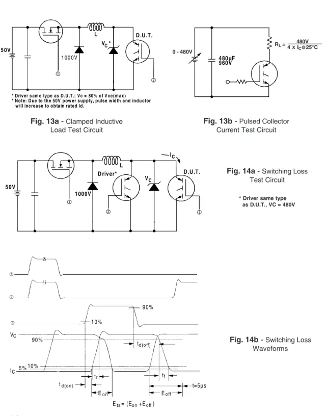
Q Repetitive rating; VGE = 20V, pulse width limited by
max. junction temperature. ( See fig. 13b )
R VCC = 80%(VCES), VGE = 20V, L = 10µH, RG = 23Ω,
(See fig. 13a)
S Repetitive rating; pulse width limited by maximum
IRG4BC30UPbF
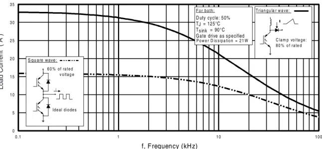
Fig. 1
- Typical Load Current vs. Frequency
(For square wave, I=IRMS of fundamental; for triangular wave, I=IPK)
Fig. 2
- Typical Output Characteristics
Fig. 3
- Typical Transfer Characteristics
0.11 1 0 1 0 0
0.1 1 1 0
C E
C
I
,
C
ol
le
ct
or
-t
o-E
m
itt
er
C
ur
re
nt
(A
)
V , C o lle cto r-to -E m itte r V o lta g e (V )
T = 1 50 °C T = 2 5°C
J J
V = 1 5 V
2 0 µ s P U LS E W ID T H G E A 0.1 1 1 0 1 0 0
5 6 7 8 9 1 0 1 1 1 2
C
I
, C
ol
le
cto
r-to
-E
m
itt
er
C
ur
re
nt
(
A
)
G E
T = 2 5 °C T = 1 50 °C
J J
V , G a te -to -E m itte r Vo lta g e (V )
A
V = 10 V 5 µ s P U L S E W ID T H C C 0
5 1 0 1 5 2 0 2 5 3 0 3 5
0.1 1 1 0 1 0 0
f, Frequency (kHz)
A
6 0 % o f ra te d v o lta g e
I
Id e al d io de s S qu are wave:
F o r b o th : D uty cycle: 50% T = 125°C T = 90°C Gate drive as specifiedsink
J
Trian gu la r w a ve: I
C la m p vo lta g e : 8 0 % o f ra te d Po w e r D is s ip a tio n = 2 1 W
IRG4BC30UPbF
Fig. 6
- Maximum Effective Transient Thermal Impedance, Junction-to-Case
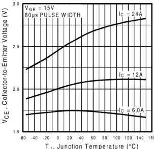
Fig. 5
- Collector-to-Emitter Voltage vs.
Junction Temperature
Fig. 4
- Maximum Collector Current vs. Case
Temperature
1.5 2.0 2.5 3.0
-60 -40 -20 0 2 0 4 0 6 0 8 0 1 0 0 1 2 0 1 4 0 1 6 0
CE
V
,
C
olle
ct
or
-t
o-E
m
itt
er
V
olt
a
ge
(
V
) V = 1 5 V
8 0 µ s P U LS E W ID T HG E
A
T , Ju n ctio n T e m p e ra tu re (°C )J
I = 2 4 A
I = 1 2 A
I = 6 .0 AC C C
0.01 0.1 1 10
0.00001 0.0001 0.00 1 0.01 0.1 1 10
t , R ectangular P ulse D ura tion (sec)1
th
JC
D = 0 .5 0
0 .0 1 0 .0 2 0 .0 5 0 .1 0 0 .2 0
S IN G L E P U L S E (T H E R M A L R E S P O N S E )
T
he
rm
al
R
es
pons
e (
Z
)
P
t 2 1 t
D M
N o te s : 1 . D u ty fa c to r D = t / t
2 . P e a k T = P x Z + T
1 2
J D M th J C C
0 5 1 0 1 5 2 0 2 5
2 5 5 0 7 5 1 0 0 1 2 5 1 5 0
Ma
x
im
u
m
D
C
C
o
lle
c
to
r Cu
rr
e
n
t (
A
T , C a se Te m p e ra tu re (°C )C
V = 1 5 V G E
IRG4BC30UPbF
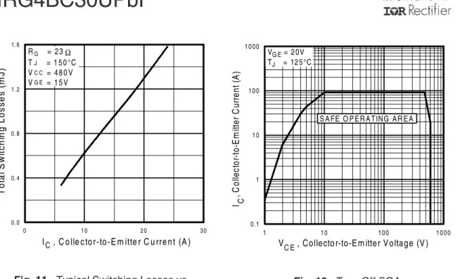
Fig. 10
- Typical Switching Losses vs.
Junction Temperature
Fig. 9
- Typical Switching Losses vs. Gate
Resistance
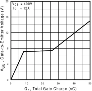
Fig. 8
- Typical Gate Charge vs.
Gate-to-Emitter Voltage
Fig. 7 -
Typical Capacitance vs.
Collector-to-Emitter Voltage
04 0 0 8 0 0 1 2 0 0 1 6 0 0 2 0 0 0
1 1 0 1 0 0
C E C , C a pac ita n ce (p F )
V , C o lle cto r-to -E m itte r V o lta g e (V )
A
V = 0V , f = 1M H z
C = C + C , C S H O R TE D C = C
C = C + C G E
ies ge gc ce res gc
oes ce gc C ies
C
re sC
oe s0 4 8 1 2 1 6 2 0
0 1 0 2 0 3 0 4 0 5 0
GE V , G ate -t o -E m itt er V ol ta g e ( V ) g
Q , To ta l G a te C h a rg e (n C )
A
V = 4 0 0V I = 12 AC EC
0.2 0.3 0.4 0.5
0 1 0 2 0 3 0 4 0 5 0 6 0
G T o ta l S w itc h in g L o ss e s ( m J)
R , G a te R e sista n ce (Ω)
A
V = 4 8 0V V = 1 5 V T = 2 5 °C I = 12 A
C C G E J C 0.1 1 1 0
-60 -40 -20 0 2 0 4 0 6 0 8 0 1 0 0 1 2 0 1 4 0 1 6 0
T o ta l S w itc h in g L o ss e s ( m J) A I = 6 .0 A I = 1 2 A I = 2 4 A R = 2 3 Ω
V = 1 5V V = 4 80 V
C C C
J
T , Ju n ctio n T e m p e ra tu re (°C )
G G E C C
IRG4BC30UPbF
Fig. 12
- Turn-Off SOA
Fig. 11 -
Typical Switching Losses vs.
Collector-to-Emitter Current
0.00.4 0.8 1.2 1.6
0 1 0 2 0 3 0
C
T
o
ta
l S
w
itch
in
g
Los
se
s (
m
J)
I , C o lle cto r-to -E m itte r C u rre n t (A )
A R = 23 Ω
T = 1 50 °C V = 48 0 V V = 15 V
G J C C G E
0.1 1 10 100 1000
1 10 100 1000
C
C E
G E
V , Collecto r-to-Em itter Voltage (V)
I
,
C
ol
le
ct
or-t
o-E
m
itt
er C
urre
nt
(A
)
S A FE O P E R A TING A R E A V = 20V
IRG4BC30UPbF
480V 4 X IC@25°C
D.U.T. 50V
L V *C
Q
R * Driver sam e type as D .U .T.; Vc = 80% of V ce(m ax)
* Note: D ue to the 50V pow er supply, pulse width and inductor w ill increase to obtain rated Id.
1000V
Fig. 13a
-
Clamped Inductive Load Test CircuitFig. 13b
-
Pulsed Collector Current Test Circuit480µF 960V 0 - 480V
RL =
t=5µs d (o n)
t
tf tr
90%
td(o ff) 10%
90%
10% 5% VC
IC
Eo n Eo ff
ts o n off E = (E +E )
Q
R
S
Fig. 14b
-
Switching Loss Waveforms 50VD river* 1000V
D.U.T. IC
C V
Q
R S
L
Fig. 14a
-
Switching Loss Test Circuit * Driver same type as D.U.T., VC = 480VIRG4BC30UPbF
LEAD AS SIGNME NTS 1 - GATE 2 - DRA IN 3 - SOURC E 4 - DRA IN B
-1.32 (.052) 1.22 (.048)
3X0.55 (.022)0.46 (.018) 2.92 (.115) 2.64 (.104) 4.69 (.18 5)
4.20 (.16 5)
3X0.93 (.037)0.69 (.027) 4.06 (.160) 3.55 (.140) 1.15 (.045) MIN 6.47 (.255) 6.10 (.240)
3.78 (.149) 3.54 (.139) A -10.54 (.415)
10.29 (.405) 2.87 (.113 )
2.62 (.103 )
1 5.24 (.600) 1 4.84 (.584)
14.09 (.555) 13.47 (.530)
3 X1.40 (.055)1.15 (.045)
2.54 (.100) 2X
0.36 (.014) M B A M 4
1 2 3
NOTES:
1 DIME NSIONING & TO LE RANC ING P ER ANSI Y14.5M, 1982. 3 O UTLINE CONF ORMS TO JE DEC OUTLINE TO -220AB . 2 CO NTROLLING DIM EN SIO N : INCH 4 HEA TSINK & LE AD M EASU RE MENTS D O NO T INCLUD E BU RRS.
H EXF ET 1- GA TE 2- DR AIN 3- SO UR C E 4- DR AIN
LEA D ASS IG N MEN TS IG BT s, CoP AC K 1- GA TE 2- CO LLEC TO R 3- EMITT ER 4- CO LLEC TO R
TO-220AB Package Outline
Dimensions are shown in millimeters (inches)
TO-220AB Part Marking Information
E X AM P L E :
IN T H E AS S E M B L Y L IN E "C" T H IS IS AN IR F 1 01 0 L OT COD E 1 78 9
AS S E M B L E D O N W W 1 9, 19 9 7 P AR T N U M B E R
AS S E M B L Y L OT COD E
D AT E CO D E Y E AR 7 = 1 9 97 L IN E C W E E K 19 L OGO
R E CT IF IE R IN T E R N AT IO N AL
Note: "P " in assem bly line
position indicates "Lead-Free"
Data and specifications subject to change without notice.
IR WORLD HEADQUARTERS: 233 Kansas St., El Segundo, California 90245, USA Tel: (310) 252-7105 TAC Fax: (310) 252-7903