Abstract— Biased and terminated p-n-p transistor chains are made from floating n-wells in p-substrate complementary metal–oxide semiconductor (CMOS) and used for power supply electrostatic discharge (ESD) clamps. The p-n-p gain may allow a compact termination circuit to be used, resulting in a stand-alone clamp. Bipolar p-n-p action accounts for unwanted low-voltage conduction as well as for very desirable clamping of power supply overvoltages. Bias networks are used to prevent excessive leakage at high temperature. These devices are becoming crucial to success in ESD product testing of CMOS integrated circuits.
Index Terms— Charged device model, Darlington transistor, diode strings, electrostatic discharge, human body model, La-grange multiplier, power supply clamp.
I. INTRODUCTION
L
ARGE numbers of pins and multiple power supplies in today’s integrated circuits (IC’s) have resulted in a very large number of electrostatic discharge (ESD) pulses in required human body model (HBM) and machine model (MM) testing [1], [2] for many products. At times, product ESD testing results do not meet expectations, despite the use of ESD protection cells which individually pass to very high ESD voltages in test patterns or on products with a simple power supply bus structure. A common theme in these failures has been separation of power supply buses in the package and resulting leakage failure after testing of the many required pin combinations. Sometimes the failure can be avoided with test partitioning, i.e., spreading the many required “zaps” over a number of components in accordance with the latest industry test standards [1], [2], but this is effective only part of the time, and of course is more costly.The common use of dual diodes for input-only protection eventually forced the issue of clamping for positive zaps to , when local supplies would occasionally fail. This was also the case for negative zaps to for virtually any signal pin. At the same time, the arrival in the CMOS process of lightly-doped drain (LDD) field-effect transistor (FET) structures and silicided diffusions weakened the ESD performance of the -channel output FET especially, and made it necessary to devise ways of protecting it. The natural dual-diode structure of the CMOS output made it possible to
Manuscript received February 15, 1996; revised April 15, 1996. This paper was presented at the EOS/ESD Symposium, Phoenix, AZ, September 11–13, 1995.
T. J. Maloney is with the Intel Corporation, Santa Clara, CA 95052 USA (email: [email protected]).
S. Dabral was with the Intel Corporation, Santa Clara, CA 95052 USA. He is now an Independent Consultant, Santa Clara, CA 95052 USA.
Publisher Item Identifier S 1083-4400(96)08375-1.
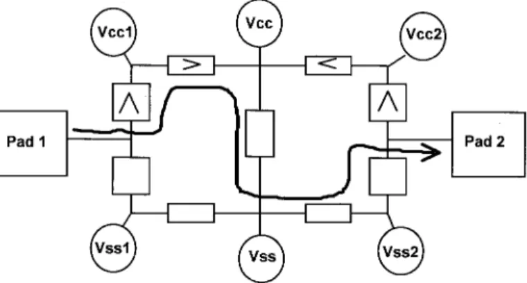
Fig. 1. Example of preferred ESD current path from one pad to another, showing passage through I/O circuits, and core power supply clamps for a positive zap. Boxes with arrows indicate strongly directional devices; others are bidirectional. It is also clear how the current path could terminate at any one of the power supply lines by passing through the elements shown.
divert some positive ESD current through the forward-biased p-channel FET (p-FET) device to the local power supply (as suggested by Fig. 1), but then required the paths between power supplies to be ESD robust. Thick-field oxide (TFO) and silicon-controlled rectifier (SCR) devices, while effective as input protection, proved to be unsuccessful as power supply clamps because of triggering difficulties and shunting of ESD current through other parts of the power bus.
When product ESD failures were often traced to the ESD current path from one power supply to another (see Fig. 1), preventing leakage failure of various power supply pins during ESD testing or actual use became a priority for IC designers. The desired “modularity” of standard cells for ESD protection was achieved when a set of standard input and output devices, known to work well on a test chip in zaps with respect to local power supplies, also worked well when properly applied to a variety of products, irrespective of power supply complexity. The modularity was achieved because an appropriate set of power supply clamping modules, discussed herein, can manage that portion of the current path and were developed as part of the ESD protection cell set. Fig. 1 shows how power supply coupling facilitates ESD current through the desired current paths for the difficult case (i.e., plenty of leakage failures have occurred with unclamped power supplies) of positive voltage applied to a signal pad. Details of the core clamping will be explained later.
This paper reports on a family of power supply clamp devices which preferentially absorb the ESD current and protect power supply pins from ESD damage. With such
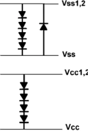
Fig. 2. Typical diode strings between peripheral and core power supplies. Note the bidirectionality of theVss1;2-Vssclamps, owing to the output NMOS transistor sources.
Fig. 3. Cross-sectional view of four-stage diode string in p-substrate CMOS.
predictable and robust paths for the ESD current, the effects of cumulative ESD stress on the parts are also less severe, which can result in lower costs and simplified qualification of the parts to all required pin combinations.
Straight diode string ESD clamps between power supply pins [3], [4] (see Figs. 2 and 3) are intended to isolate the core and supplies from noisy output power busses and . Reference [3] discusses how up to four series diodes can be advisable for noise isolation between supplies at the same nominal voltage. Diode strings are commonly built in floating n-wells in p-substrate CMOS and are actually p-n-p transistors (Fig. 4) because the common substrate acts as a collector. The single diode on the clamps is, of course, the n junction on the p-substrate, while the stack of four is a diode string cell. Also shown in Fig. 2 is a typical diode string between or and a core . Notice that the - arrangement is bidirectional (because of the parasitic diode), while the - coupling is unidirectional, in agreement with the notation in Fig. 1.
These diode strings have demonstrably improved ESD per-formance for HBM and MM ESD tests, as described in [3] and [4]. In their role as “charge couplers” [5], they have enhanced charged device model (CDM) performance as well. But there is still a need for a comprehensive stand-alone clamp in cases where 1) requirements of power-up sequencing or 2) planned differential voltages require it. Also, straight diode strings can be used to clamp core [4] only if the target voltages (including high temperature burn-in) are very low.
Fig. 4. Four-stage diode string of Fig. 3, seen as a chain of p-n-p transistors.
For all cases of diode strings discussed herein, the devices are built on epitaxial CMOS with a conducting p substrate. Diode strings have also been successfully built on n substrate epitaxial CMOS. All the basic concepts in this paper will thus be discussed in terms of the p-n-p vertical transistor in n-well, p-substrate CMOS. It will be shown that the collection of ESD current by the p substrate , directly beneath the diode string structures, is of considerable importance and contributes to the favorable results.
As described in [3], [4], and recently in [6], the diode string’s p-n-p gain results in loss of forward current to the substrate, especially at high temperatures, thus reducing the voltage across “downstream” diodes and increasing the cur-rent requirement for a given voltage. Also, the p-n-p chain amplifies junction leakage of the downstream -wells.
Here, we present some methods for minimizing the current requirement in diode strings, as well as a method for utilizing the p-n-p gain of a diode chain for stand-alone ESD protection [7]. We will begin with the design improvements relating to leakage of diode strings “bridging” two supplies. Then we will continue by modeling the ESD current regime, and developing the concept of a self-terminated, stand-alone diode string clamp.
II. P-N-P-BASED DIODE BEHAVIOR IN THE LEAKAGE CURRENT REGIME
One can begin with such references as [8] and show, as was done in [3] and [4], that if a silicon diode forward voltage at absolute temperature is known, the voltage at the same forward current can be calculated for another temperature
(1)
where V and is the diode ideality factor. The temperature coefficient of will thus be negative; typically is room temperature and is around 0.55–0.65 V for forward current of 1–10 A, giving a temperature coefficient for around 2.2 mV/K, and directing our attention to the higher temperatures.
Diode ideality factor can be measured from a semilog plot of diode versus . An ideal diode gives the well-known 60 mV/decade slope for low currents at room temperature. Once the single diode ideality factor is determined, the semilog – slope of a diode string is of interest. For a series of diodes, it can be shown that the low current – slope is
volts per decade
Fig. 5. Current gain effects in the p-n-p bipolar transistor formed by a diode stage.
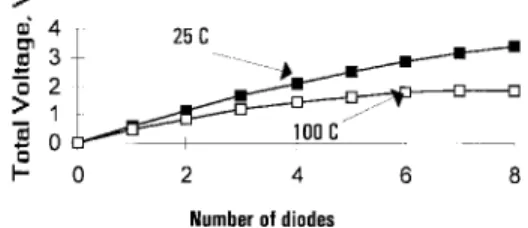
Fig. 6. Diode string turn-on voltage for two temperatures for = 6.
bipolar current gain just amplifies the current passed at a given voltage, in a manner depending only on itself.
Now we consider the effect of the p-n-p bipolar current gain, or , on the performance of the diode string. A single stage of the Darlington-coupled series is shown in Fig. 5, with the usual relations shown for emitter, base, and collector currents. Because the next diode stage has reduced current flowing into its emitter, the forward voltage in stage 2 will be reduced by an amount depending on
(2)
so that
or
Now let , 60 mV for an ideal diode at room . The analysis of (2) is applied to multiple stages to give a loss of an additional at each stage, resulting in a total voltage of a string of identical diodes at current of
(3)
where is the base-emitter voltage for one diode (collector and base shorted) at emitter current . This result also appears in [3], [4], and [6]. Obviously this model depends on a constant and no effect of series resistance, which are usually the case in the low leakage current range. The effect of temperature on diode string efficiency is clearly seen in Fig. 6, which plots out (3) for two temperatures.
But (3) is the total diode string voltage for a set of identical diodes. Now suppose the area of each succeeding p-n-p stage of a diode string shrinks by exactly a factor of
Fig. 7. Log of current gain versus log of emitter current density for a typical diode string p-n-p transistor, allowing simplified modeling of the diode string performance. The coefficientn is measured for each process.
. Then, the current density at each diode is exactly the same, and the full voltage of is achieved across the chain. Equation (3) can be seen as a special case of
(4)
where is the diode area of the th stage relative to the first stage, i.e., . The second term will therefore vanish, or at least be reduced, if the diode/p-n-p chain is tapered to some extent, in accordance with the expected value of . A properly tapered diode string not only removes the isolation voltage problem associated with , it uses less area. But tapering introduces more series resistance, which has a substantial effect on the ESD current regime. The right dimensions for diodes in a diode string are largely determined by detailed modeling of the ESD current regime, yet to be considered.
III. P-N-P-BASED DIODE BEHAVIOR IN THE ESD CURRENT REGIME
When an ESD pulse passes through the diode/transistors, the current density is many decades higher than in the leakage regime discussed above. Now there are not just microamps of leakage, but milliamps per micron of p finger length in the initial diode stage. In this regime, diode resistance effects become important, and current gain decreases. In the high-current p-n-p diode model, we find that high-current density is adequately expressed by current per micron of p finger length in the diode stage. Such fingers are usually drawn with a particular style in a given process, with minimum dimensions and strongly connected with contacts and metal. Thus, it has become common practice for us to characterize diode “area” for a given process in terms of p finger lengths in a diode stage.
allows ESD current to pass to the substrate. also always increases with temperature, which is undesired for leakage. Despite these multiply undesirable conditions, we will show that it is possible to design competitive protection devices within the available area. Since the diode current is reduced by a factor of after stages, even such low values of result in much of the ESD current being shunted to ground. We have measured the versus for a number of processes using diode string single cells. Representative values for two processes are shown in Table I. Note that when the overall value of is lower, it tends to decline more gently at high currents (lower coefficient ). The values of for the processes given in Table I are asymptotic, but the entire curve can be constructed very accurately by taking the harmonic average (reciprocal of the sum of reciprocals) of the low and high current values at each value of current density. The processes at our company are such that we have no experience with between values of seven and 30, so the reader is referred to other sources [6] for studies of the transition from low to high .
The model for the ESD current regime employed in our Diodes and Darlingtons (DIDAR) spreadsheet computer pro-gram uses the same information as the low current model, but breaks the device into stages so that the effects of resistance and current-varying can be included. One must start with an input current and device size so that these effects can be prop-erly scaled. The spreadsheet then computes the current path and voltage drop for each stage using a modified Ebers–Moll bipolar transistor model, where the collector conductance (e.g., 7 mS/ m) and versus current density are considered. Details of the spreadsheet calculations will not be presented herein to save space, but such a discussion is found in the original conference paper [10]. Modeling results do give remarkable agreement between theoretical and experimental pulsed – , enabling us to use the computer model to optimize diode layouts.
Another feature of transistor behavior which is not consid-ered in this model is charge storage in the base, which adds a capacitive element to the circuit model. Pulse measurements on diode strings have indicated that considerable charge storage occurs, but that it is harmless and even helps the device to absorb ESD charge as intended.
IV. MANAGING ANDEXPLOITING WITHCIRCUITDESIGN
In the last section we discussed the following:
1) that low-current is a nuisance because it cuts the turn-on voltage of the chain;
2) that high-current is of great benefit because it turns the diode string into a very effective power supply clamp to substrate , surpassing its role as a mere conduit for charge to another power bus. Although is unfortunately higher at low currents, there still are ways to use for ESD clamping while minimizing its effect on diode string performance in the leakage regime. In this section, we will outline these techniques, the goal of which is to eliminate the unwanted effects of without compromising ESD performance.
TABLE I
MEASUREDMODELPARAMETERS FORVARIOUSPROCESSES. GENERALLY, THEHIGHCURRENTDENSITYVALUE OF CANBEEXTRAPOLATED TOLOWCURRENTSUNTIL IT IS LIMITED BY THELOWCURRENTDENSITY(MAXIMUM) VALUE
Fig. 8. Bias network for a six-diode mixed power supply clamping string, designed to maximize the temperature at which leakage current of
1V=R = 2:5=R flows, while using minimum total resistance.
A. Bias Networks and Cladded Diodes
The reason for the declining incremental voltage across the diode string is, of course, lower current density in the latter stages, due to current flow to ground. Boosting current density in the latter stages so that the total desired voltage drop is partitioned more or less equally among the available stages is, therefore, a worthy goal. Tapering accomplishes this, but the main problem with tapering is that using this method to minimize leakage in a diode string is not compatible with maximizing ESD performance, as discussed above. But there is another method to lift the sagging curves of Fig. 6 without affecting ESD performance at all, by augmenting the diode string with a bias network to distribute small but significant forward current to the diodes.
How best can we distribute bias current? We would like to distribute current to the various diodes in the string so that total voltage is maximized for a given current, i.e., the sum of diode voltages is maximized subject to the constraint of the total current sum equal to a constant. For a constant , the method of Lagrange multipliers can thus be applied (see Appendix) and it can be shown that 1) for , equal currents in all diodes, regardless of size, maximize the voltage, and 2) for any , diode currents (beginning at positive end of string) should be
and
(5) with being the total current.
Such approximate equalization of currents is the goal of an ideal bias network We can approach this ideal with various practical realizations.
Fig. 9. Measured leakage for 3.0–5.5 V six-stage cladded diode string, with discrete resistors as in Fig. 8. Values were chosen to allow low leak-age up to 100 C.
Fig. 8 shows a biased diode string with the extremes of 3.3–5 V mixed power supplies applied. In Fig. 8, the usual chain of p-n-p transistors is pictured as diodes with a dis-tributed ground as the common collector. We minimize the area used by minimizing the total resistance involved, as well as the total number of resistors. The most efficient choice for a resistor is the long-channel p-FET device.
The objective is to come close to equalizing currents by equalizing voltages since the diode sizes are, logarithmically speaking, about the same. In order to achieve the desired 2.5 V across the string in Fig. 10 at a given temperature (say, 100 C), we calculate what current is required by two p-n-p diode/transistors biased at V at that high target temperature. Then we choose so that flows through each pair of diodes, i.e., and is the total leakage (assume infinite p-n-p gain, worst case). The first resistor carries the current for the second and third diode pairs, the second resistor the current for the last diode pair, and equal voltages appear across each pair. Thus the total current through the diode string is or less.
If the cladded diode string is generalized to eight diodes in segments of two, the (simplified) total current is , but this is now , where into a segment produces , or 2.5/4 V in this case, and the resistor series is . The pattern developing is clear; for equipartition of voltage into equal segments of a diode string, the resistor sequence is
starting from the positive end of the string. The resistor sequence, starting from the right, follows what mathematicians call the harmonic series: .
Total current will not exceed as long as forcing through a segment produces at least V. A more complete discussion of these biasing concepts and other material in this section can be found in [7] and [10].
Fig. 9 shows results of experimental idealized cladded six-diode strings, arranged with discrete megohm resistors, wired
Fig. 10. Cladded bias network implemented in p-channel FET’s for a six-diode mixed power supply clamping string, intended for a process limited to 3.6 V across gate oxides.
as in Fig. 8. Again, 3–5.5 V is applied. The advantage of the bias network is seen to be substantial at the high temperatures, while the 1 A or so of leakage current persists down to low temperature because of the resistors.
The cladded diode string resistors are implemented on-chip with p-channel FET’s, as shown in Fig. 10. Fig. 10 shows the design of a mixed voltage 3.3–5 V cladded string for a process where gate oxide voltages greater than 3.6 V are not allowed, thus the p-channel resistor gates are referred to 3 V. This even allows smaller p-channel devices to be used because the conductance is lower than if the gates were at 0 V. The resistive connections to 3 V and 0 V prevent unimpeded power supply voltages from appearing across a thin gate oxide. The resistive connection to (ground) is accomplished with an n-channel device; otherwise, there would be a power supply voltage across a gate oxide.
Fig. 11. Six-stage p-channel cladded diode stringI versus T for Fig. 12, compared with unbiased current as calculated from individual cell data.
Fig. 12. Use of a buffered voltage divider to supply extra bias current to the middle of a long diode chain.
goes up with temperature. More advanced processes tend to have even lower and operate at even lower supply voltages, and the voltage steps downward become smaller as well. The need for biasing these mixed-voltage diode clamps could thus be reduced if the higher supply voltage on a chip goes back only one previous generation.
The resistive bias network offers another benefit to operation of the Darlington p-n-p transistor chain, that of supplying leakage current to the floating n-wells (transistor bases) distant from the highest voltage power supply. This is especially important at high temperature. Although n-well leakage is usually no higher than a few nanoamps even at high operating temperature, it is important to avoid supplying that current to the remote n-wells through several amplifying p-n-p stages; the total leakage becomes the basic leakage multiplied by several factors of . With the configuration of Figs. 8 and 10, the floating n-well leakage is fed through at most one p-n-p stage, so total leakage due to that effect is kept low. Even at room temperature and equal voltages this issue can become severe when the diodes are exposed to light (particularly a microscope light during failure analysis!), because then the n-well “leakage” is a quite considerable photocurrent. A photo-Darlington effect results and the -current is huge because the photo-current has to be supplied through an amplifier. A proper bias network can reduce total current and not confuse the failure analyst.
The voltage applied across the biased diode string could also be between a and a , for example, with core being the most likely choice. As technology advances and IC’s run at lower and lower voltages, with correspondingly lower
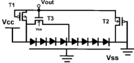
Fig. 13. Boosted diode string as achieved with buffered voltage divider in the form of long-channel leaker pair T1 and T2, and source follower T3, supplying extra bias current to the middle of a long diode chain only when needed.
burn-in voltage, this kind of power supply clamp has been considered [4]. A chain of eight diodes, for example, can be arranged to clamp a 2.5–3 V supply with low leakage, and also survive 3–3.6 V burn-in to high temperatures (from 125 C to 150 C), at least with the rather low p-n-p values seen in advanced technologies.
With such a long diode chain sustaining its largest differen-tial voltage at burn-in (at which temperatures the p-n-p goes up), some method of pumping extra current into intermediate stages is still desired. But the current replenishment at high temperatures and burn-in voltage could severely compromise the product performance at lower temperature and lower voltage unless some improvement is made to the biasing schemes discussed thus far. The following idea offers an answer.
B. Bias Networks and Boosted Diodes
Fig. 14. I versus T for eight-stage diode string as in Fig. 13, shown with and without booster network enabled. This circuit is intended as a Vcc
clamp for a low-voltage process.
Fig. 15. PulsedI–V measurements for boosted eight-stage clamp, and comparison with model prediction.
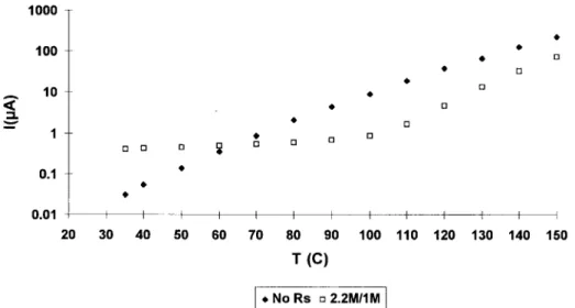
current through the divider to be small, and for the amplifier to supply little current from unless needed, e.g., at high temperatures. This would then lower the leakage current as shown in Figs. 9 and 11 at all temperatures, at the cost of a little extra circuitry. Fig. 13 shows how such a scheme is implemented in CMOS circuitry. The leaker pair and are always on, but as very long channel devices do not draw significant . When the node following the fourth diode falls a threshold below , as at high , the source follower (a stronger device, capable of many microamps of current) turns on until the lower part of the chain is replenished adequately. But is off completely or sourcing very small currents at lower temperatures, where is easily supported at low currents. The body effect in affects its trip point, but the leaker pair is designed with that in mind.
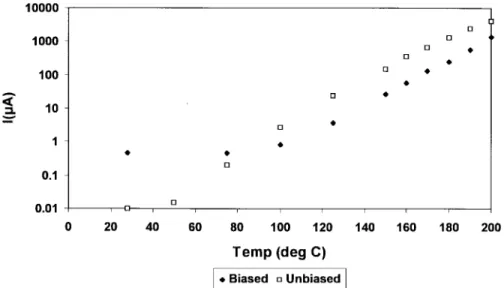
Fig. 14 shows experimental results for an eight-stage boosted diode as in Fig. 13. Results are shown with and without the bias network enabled, revealing a factor of three or more improvement with the bias network for the
higher temperatures, where current becomes substantial. The background current (due to the voltage divider) at low temperatures is submicroamp but could be reduced further by lengthening the transistor channels in the voltage divider. Note that, unlike the cladded clamp, the advantage over an unbiased string persists out to very high temperatures because of controlled current sourcing by the active element.
C. Cantilevered Diodes
Diode tapering recognizes that less and less current is required by each succeeding stage of the diode/p-n-p chain. This fact is useful in other ways, as we consider once again the p-n-p chain as pictured in Fig. 3. Because of the current gain at each stage, the current at the output is a factor of less than the input current. Thus, even for a fairly low , the majority of the current flows to the substrate. For a modest , even one less than ten, the base current required at the output is low enough that we can consider alternatives to attaching the output to another power supply. Some kind of small circuit should be sufficient, and would free the user from assuring that the two power supplies always track within the voltage limits. The concept of not having a power supply anchorage at the far end of the diode chain has come to be known at our company as cantilevered, or cantilever, diodes. It can be combined with diode tapering and bias networks to produce more efficient, more versatile diode string designs.
The architectural advantages of cantilever diodes are con-siderable. Even if 3.0–5.5 V or other mixed-power supply differences can be withstood by a well-designed diode/p-n-p string at all temdiode/p-n-peratures, diode/p-n-powerudiode/p-n-p sequencing odiode/p-n-ptions may prevent it from being used in a given product. Also, a stand-alone diode scheme is desired to protect core . While core is usually the best on the chip and very ESD-tolerant, this is not always the case [11], [12], and small core are known to perform very poorly at times. A good core power supply clamp can forgive the kind of obscure weaknesses discussed in [11] and [12], and in related cases, and free us from a great deal of failure analysis and redesign.
A simple capacitor at the output might be a sufficient termination for cantilever diodes, but it must be reset after every pulse or it will charge up and turn off the diode string. This is because of the repeated pulses of the HBM test, where power supplies are (directly or indirectly) stressed seconds apart for hundreds or thousands of times. A capacitor needs a small pullup diode to the input in order to discharge within one second.
A cantilevered diode termination that sinks a substantial amount of base current over the time of an ESD pulse, but which turns itself off long term, is shown in Fig. 16. Base current, usually up to tens of milliamps, is sunk through the short channel (perhaps 200/1) p-FET , whose gate is initially grounded because of the capacitor. The thin oxide capacitor is a few picofarads and is pulled up by a long-channel p-FET with an equivalent resistance in the megohm range, to give an RC time constant of microseconds. The other two p-FET’s are also long-channel devices, and supply leakage current to critical points, avoiding the amplified leakage problem. The small n-FET provides a ground without allowing a power supply voltage across a single thin gate oxide. Also shown is a symbol used for the entire circuit in diagrams of power bus clamping schemes.
After the RC-induced time delay, turns off and there is no long-term conduction to ground. ’s p-diode to the input assures that the capacitor voltage does not go higher than the input, as it would with repeated pulses if there were no such
Fig. 16. Six-stage cantilevered diode string with resistive bias network and termination circuit. The suggested circuit symbol could apply to any cantilever clamp network.
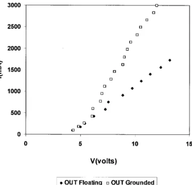
Fig. 17. PulsedI–V curves for six-diode cantilevered string in process P2
(see Table I); OUT floating includes the required termination circuit, and OUT grounded indicates how much voltage develops across that circuit as well as the six-diode I–V relation.
diode. The circuit thus relaxes after each pulse due to leakage
on .
The ESD current regime is demonstrated in Fig. 17, which shows pulsed – curves for a cantilever design resembling that of Fig. 16. Data were taken with 100 ns transmission line pulses [13], resembling the time scale and current level of HBM and MM ESD events and simulation tests. The upper curve, with OUT (see Fig. 16) grounded (representing the – of a six-stage diode string), can be subtracted from the lower curve at a given current to indicate the voltage developed across the -FET termination. This cantilever design, about the size of 2–3 bond pads, is seen to sink over 1.3 A at 12 V, meaning that it can sink the maximum current of a 2 kV HBM pulse before the voltage rises to a level known to cause power supply leakage on this process when short pulses are applied. The current sinking of the cantilever clamp is additive, of course, and so we can protect to much higher HBM voltages with multiple placements of the cell.
Fig. 18. n-FET termination for cantilever clamp. The diode bias network is also shown.
case, the long-channel devices need only be long enough not to interfere in the ESD current mode. A 1/5 m FET is quite acceptable, and several of these can be built into the same n-well to . Under these conditions, the leakage current obeys the same Arrhenius relation as ordinary junction leakage and can be kept on the nanoamp scale at product temperatures of 100 C, while one microamp is not reached until 200 C. Even with networks having some leakage amplification as in Fig. 16, 1 A is not exceeded until 160 C. In all cases, it is quite easy to design bias networks with enough strength to stabilize the cantilever device to over 200 C. As long as the leakage is less than 1 A at 100 C, there is no difficulty meeting product leakage current requirements even for battery-operated devices.
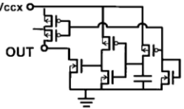
A number of alternative cantilever clamp terminations have been proposed [7]; one of the several that have been success-fully fabricated and tested is shown in Fig. 18. In this version, the usual RC circuit is followed by an inverter with a high trip point, which drives the gate of an n-channel FET (n-FET). Thus, the n-FET termination has gate drive without necessarily dropping voltage, giving more current per volt developed in series with the diodes. But in a side-by-side comparison of pulsed – for cantilever clamps on the process, the voltage saving with the -FET cantilever termination was small. This kind of termination was also successful when the n-FET termination was replaced with an npn bipolar transistor in a BiCMOS process.
An alternative to Fig. 18 for the n-FET termination is to eliminate the inverter and have the capacitor to and the long-channel p-FET resistor to ground, but this was avoided due to concerns about noise coupling from . Other successful termination schemes include a two-stage complementary RC network [14] as described in [7], which is applicable to p-FET or n-FET terminations.
The termination circuit of Fig. 18, exclusive of the bias network, resembles the n-FET-only power supply clamp circuit suggested by Merrill and Issaq [15], but the latter’s n-FET is about 40 times larger (at 8000 m) and passes all the current. While most of our cantilever clamps have about six diode stages, like Fig. 16, the optimal solution for a power supply clamp is obtained through modeling and depends on diode model parameters, voltage targets, and area constraints. There is a continuum of possible power supply clamps ranging from the all-n-FET solution of [15] to long strings of diodes with minimal terminations. Optimal design suggests use of the superior transconductance of the p-n-p bipolar stages until the cost of another diode voltage drop is more than a MOSFET termination for the rest of the current. Low-voltage processes,
across two thin oxides instead of one. Methods for adapting the cantilever diode circuits to this are described elsewhere [7] and are beyond the scope of this work, but they make use of the same voltage-division methods as described above for cladded and boosted diode string networks.
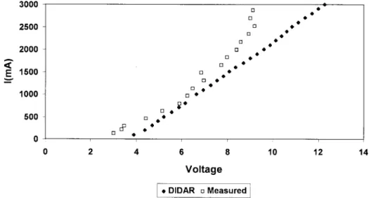
The high-beta process (see Table I) can be used to make very efficient cantilever diode clamps, as seen in the pulsed – results of Fig. 19. The predicted – from the DIDAR spreadsheet modeling of this six-stage clamp (again, using measured single cell values of and versus current density) is seen to be conservative. Process includes 12 V programming pins, meaning that power supply damage does not occur until several volts above 12 V. This cantilever clamp, 125 335 m or again about the size of 2–3 bond pads, is thus easily capable of sinking the current of a 4–5 kV HBM pulse by itself. This amount of space has not usually been a hardship, although sometimes designers have reshaped the cell to fit in the available area. Technology scaling has actually helped for high processes; in a shrunk version of , still 12-V compatible, a similar result was obtained for a 180 150 m cantilever cell. The diode -finger lengths in the six stages were tapered from about 750 m in the first stage, down to 120 m in the last.
V. DISCUSSION
First, let us summarize the cantilever diode concept. The cantilever diode chain shunts ESD charge because it turns on whenever the voltage on its input connection is suddenly raised. This is why it does not make a good input protection device to ground—it is like an ac short circuit to any changing signal. As a power supply clamp, the diode chain has no trigger voltage or overshoot problem, and should be fine as long as the startup transient is acceptable. Fortunately, ESD charge for the HBM is on the order of 100 pF 2000 V C, and for the CDM and MM is even less, so the diode/p-n-p string conducts on the order of microcoulombs to serve as an effective ESD clamp. As 3.6 C is A-h, or about of a battery charge, the startup transient is of minor concern for product operation and for most startup transients, which last milliseconds.
Fig. 19. Measured and modeled pulsed I–V curves for cantilever clamp in the process P1.
is usually enough gain available from a multistage p-n-p chain to allow output base current to be supplied by a small circuit. Because they provide a defined path for ESD current be-tween power and ground, cantilever diode clamps, and diode clamps in general, remove the uncertainty from ESD protection schemes which pass current to a power supply bus. Since the ESD current does not go through undesired breakdown paths from to , damage due to wearout or unexpected weak-ness in the power supply bus does not occur, with the result that components can survive hundreds or thousands of ESD zaps. This can result in lower costs and simplified qualification of the parts to all required pin combinations. When cantilever diode power clamps are used, HBM performance above 4 kV is routinely observed in large, multi- products, even without changing samples.
The diode clamps described herein (cladded, boosted, cantilever) achieve ESD protection as well as temperature-dependent voltage–current goals by using the associated networks and biasing schemes. While the Darlington transistor is not new [16], the primary applications have been not with ESD protection but with the (usually two-stage) Darlington used for amplifying signals in bipolar IC’s [17], [18]. In this application, bias resistors (between the emitter of the first transistor and the base of the second) are placed primarily to speed up the device, and incidentally to avoid amplified leakage current [17]. The multistage Darlington configuration has sometimes been discussed in the literature as a power device [19], but mostly in theoretical terms. They are probably too slow to compete with today’s power MOSFET’s because of charge storage in the bases, but that charge storage can only help ESD performance.
The history of semiconductor devices, and of electronics in general, is replete with cases of using the available gain to solve any and all problems. This Darlington-coupled series of p-n-p transistors is a gain block, but it would perform poorly as a traditional amplifier, as discussed above, and as such has not been a common sight in chip design. But, because of its current gain, it is beginning to help solve a major ESD protection problem, that of multiple power supply clamping. Because of
their “stand-alone” status and ease of application, cantilever diode clamps have become important for power supply ESD clamp in most Intel processes. At the same time, diode strings cross-coupling supplies are still advantageous, and their utility is enhanced by use of the cladding and boosting bias schemes which minimize leakage current.
VI. CONCLUSION
We have presented a variety of techniques for implementing diode strings to open up a defined ESD current path between integrated circuit power supplies. Diode strings built in p-substrate CMOS become chains of p-n-p transistors with high bipolar current gain and may need to be accompanied by additional circuitry in order to meet leakage current goals. These additional circuits are bias networks in the form of long-channel transistors and, sometimes, small active devices. While the bipolar p-n-p action in diode strings accounts for some difficulties with them, it also offers improved perfor-mance and flexibility. On balance, the p-n-p bipolar action has no real drawbacks and is highly exploitable for ESD protection when these design methods are used.
Fig. 20. Currents in p-n-p diode strings with bias.
Diode strings in these form provide a convenient modular solution to ESD design and help assure that input and output circuits which perform well for test patterns will perform well in a product. All of the diode strings are easily characterized with pulsed – measurements, allowing the designer to solve the complete ESD circuit model for the product, and prove that the ESD pulse will preferentially flow through the diode clamp. By implementing these kind of designs in the ESD current paths of a product, high ESD performance to all required pin combinations can be achieved.
APPENDIX
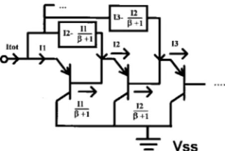
The goal of applying an optimized bias to intermediate points in a p-n-p diode string can be expressed by the desire to maximize total voltage across the string for a given total current. The current supplied is the sum of the current into the first diode, plus any bias current applied to intermediate points. Currents are defined as in Fig. 20. is defined as the total current entering the th p emitter and is taken to be constant, as is usually the case in the leakage regime. Note that bias current is added to the current transferred from the previous stage due to finite , and the total current is plus all the bias currents.
The problem can be solved through the method of Lagrange multipliers [20]. The total current is
or
(A1)
We want to maximize total voltage
subject to equal to a constant. Since is constant, an appropriate constraining function is
(A2)
where and is proportional to
diode area. Then applying the method of Lagrange multipliers
This gives , and .
Substituting back into (A1), this gives
and of course
(A4)
The solution for indexed is left to the reader, but is easily seen to involve current ratios in terms of the respective .
ACKNOWLEDGMENT
This work began at Intel in the first quarter of 1993. The authors acknowledge early discussions with A. Volk and R. Aslett which were particularly helpful. Other contributors include J. Blacker (who also formulated the cantilever clamp symbol in Fig. 16), J. Falk, E. Grant, M. Isbara, K. Parat, and G. Wagner. E. Abratowski, T. Cantarero, and B. Payne performed many of the laboratory measurements which appear here. Finally, the authors thank the Intel product Q&R Depart-ments and their product ESD testing. Their constant testing, failure analysis, and reporting helps to establish the priorities for fundamental design improvement.
REFERENCES
[1] ESD Sensitivity Testing: Human Body Model (HBM)-Component Level, ESD Association Standard, S5.1, 1993.
[2] ESD Sensitivity Testing: Machine Model (MM)-Component Level, ESD Association Standard, S5.2, 1994.
[3] S. Dabral, R. Aslett, and T. Maloney, “Designing on-chip power supply coupling diodes for ESD protection and noise immunity,” in EOS/ESD
Symp. Proc., 1993, pp. 239–249.
[4] , “Core clamps for low voltage technologies,” in EOS/ESD Symp.
Proc., 1994, pp. 141–149.
[5] T. J. Maloney, “Enhancedp+substrate tap conductance in the presence of NPN snapback,” in EOS/ESD Symp. Proc., 1990, pp. 197–205. [6] S. Voldman and G. Gerosa, “Mixed-voltage interface ESD protection
circuits for advanced microprocessors in shallow trench and LOCOS isolation CMOS technologies,” in IEEE Int. Electron Devices Meet.
Proc., 1994, pp. 277–280.
[7] T. J. Maloney, “Electrostatic discharge protection circuits using biased and terminated p-n-p transistor chains,” Intel, Santa Clara, CA, U.S. Patent 5530612, filed Mar. 28, 1994, issued June 25, 1996.
[8] Y. P. Tsividis, “Accurate analysis of temperature effects in Ic-Vbe
characteristics with application to bandgap reference sources,” IEEE
J. Solid State Circuits, vol. SSC-15, pp. 1076–1084, Dec. 1980.
[9] W. M. Webster, “On the variation of junction-transistor current am-plification factor with emitter current,” in Proc. IRE, June 1954, pp. 914–920.
[10] T. J. Maloney and S. Dabral, “Novel clamp circuits for IC power supply protection,” in EOS/ESD Symp. Proc., 1995, pp. 1–12.
[11] C. Duvvury, R. N. Rountree, and O. Adams, “Internal chip ESD phenomena beyond the protection circuit,” in Proc. IEEE Int. Reliability
Phys. Symp., 1988, pp. 19–25.
[12] C. C. Johnson, S. Qawami, and T. J. Maloney, “Two unusual failure mechanisms on a mature CMOS process,” in EOS/ESD Symp. Proc., 1993, pp. 225–231.
[14] A. M. Volk, Intel Corporation, private communication.
[15] R. Merrill and E. Issaq, “ESD design methodology,” in EOS/ESD Symp.
Proc., 1993, pp. 233–237.
[16] S. Darlington, “Semiconductor signal translating device,” U.S. Patent 2 663 806, Dec. 22, 1953.
[17] P. Horowitz and W. Hill, The Art of Electronics, 2nd ed. Cambridge, England: Cambridge Univ. Press, 1989, pp. 94–95.
[18] P. Gray and R. Meyer, Analysis and Design of Analog Integrated
Circuits, 3rd ed. New York: Wiley, 1993, p. 223.
[19] C. Wheatley and W. Einthoven, “On the proportioning of chip area for multi-stage darlington power transistors,” IEEE Trans. Electron Devices, vol. ED-23, pp. 870–878, Aug. 1976.
[20] G. B. Thomas and R. L. Finney, Calculus and Analytic Geometry, 5th ed. Reading, MA: Addison-Wesley, 1979, pp. 620–627.
Timothy J. Maloney (S’74–M’76–SM’84) received
the S.B. degree in physics from the Massachusetts Institute of Technology, Cambridge, in 1971, the M.S. degree in physics from Cornell University, Ithaca, NY, in 1973, and the Ph.D. degree in elec-trical engineering from Cornell in 1976.
In 1977, he joined the Central Research Labora-tory of Varian Associates, Palo Alto, CA. At Varian until 1984, he worked on III-V semiconductor pho-tocathodes, solar cells, and microwave devices, as well as silicon molecular beam epitaxy and MOS process technology. Since 1984, he has been with Intel Corp., Santa Clara, CA, where he has been concerned with integrated circuit ESD protection, CMOS latchup testing, fab process reliability, and design and testing of standard IC layouts. He is now a Principal Engineer at Intel. He has taught short courses at the University of California at Los Angeles, the University of Wisconsin, Madison, and the University of California at Berkeley.
Dr. Maloney received Best Paper Awards for his contributions to the EOS/ESD Symposium in 1986 and 1990, was General Chairman for the 1992 EOS/ESD Symposium, and received the ESD Association’s Outstanding Contributions Award in 1995. In 1994, he was named to receive the Intel Achievement Award for his patented ESD protection devices, which have achieved breakthrough ESD performance enhancements for a wide variety of Intel products. He is a member of the Electrochemical Society.
Sanjay Dabral (M’93) received the B.Tech. degree
from the Indian Institute of Technology, Madras, India, in 1986, the M.S. degree from Clemson University, Clemson, SC, in 1988, and the Ph.D. degree from Rensselaer Polytechnic Institute, Troy, NY, in 1992.