HCS12
Microcontrollers
"CONTROLLED COPY"
S12DBGV1/D Rev. 1.01
Debug (DBG)
Module V1
Block User Guide
PRINTED VERSIONS ARE UNCONTROLLED EXCEPT WHEN STAMPED
"CONTROLLED COPY"
IN RED
Block Guide — S12DBG V1
Motorola and the Stylized M Logo are registered trademarks of Motorola, Inc. DigitalDNA is a trademark of Motorola, Inc.
This product incorporates SuperFlash® technology licensed from SST. © Motorola, Inc., 2003
Revision History
Version Number
Revision Date
Effective
Date Author Description of Changes
PRINTED VERSIONS ARE UNCONTROLLED EXCEPT WHEN STAMPED
"CONTROLLED COPY"
IN RED
Block Guide — S12DBG V1
List of Figures
Figure 1-1 DBG Block Diagram in BKP Mode. . . 8
Figure 1-2 DBG Block Diagram in DBG Mode . . . 9
Figure 3-1 Debug Control Register (DBGC1) . . . 16
Figure 3-2 Debug Status and Control Register (DBGSC). . . 18
Figure 3-3 Debug Trace Buffer Register (DBGTB) . . . 19
Figure 3-4 Debug Count Register (DBCNT) . . . 20
Figure 3-5 Debug Comparator C Extended Register (DBGCCX) . . . 21
Figure 3-6 Comparator C Extended Comparison in BKP/DBG Mode. . . 22
Figure 3-7 Debug Comparator C Register (DBGCC) . . . 22
Figure 3-8 Debug Control Register 2 (DBGC2) . . . 23
Figure 3-9 Debug Control Register 3 (DBGC3) . . . 24
Figure 3-10 Debug Comparator A Extended Register (DBGCAX) . . . 27
Figure 3-11 Comparators A and B Extended Comparison in BKP Mode . . . 28
Figure 3-12 Debug Comparator A Register (DBGCA) . . . 28
Figure 3-13 Debug Comparator B Extended Register (DBGCBX) . . . 29
"CONTROLLED COPY"
IN RED
List of Tables
Table 2-1 External System Pins Associated With DBG and MEBI . . . 13
Table 3-1 DBG Register Summary . . . 15
Table 3-2 CAPMOD Encoding . . . 18
Table 3-3 Trigger Mode Encoding . . . 19
Table 3-4 CNT Decoding Table . . . 20
Table 3-5 PAGSEL Decoding . . . 21
Table 3-6 Comparator C Compares. . . 22
Table 3-7 Breakpoint Mask Bits for First Address . . . 25
Table 3-8 Breakpoint Mask Bits for Second Address (Dual Mode) . . . 25
Table 3-9 Breakpoint Mask Bits for Data Breakpoints (Full Mode) . . . 26
Table 3-10 Comparator A or B Compares . . . 28
Table 4-1 Read or Write Comparison Logic Table. . . 34
Table 4-2 Resolution of Mode Conflicts . . . 37
Table 4-3 Breakpoint Setup . . . 40
Section 1 Introduction to the Debug (DBG) Module
1.1 Overview. . . 11.2 Features . . . 4
1.3 Modes of Operation . . . 6
Section 2 External Signal Description
Section 3 Memory Map/Register Definition
3.1 Register Descriptions . . . 103.1.1 Debug Control Register 1 (DBGC1). . . 10
3.1.2 Debug Status and Control Register (DBGSC) . . . 12
3.1.3 Debug Trace Buffer Register (DBGTB) . . . 13
3.1.4 Debug Count Register (DBGCNT) . . . 14
PRINTED VERSIONS ARE UNCONTROLLED EXCEPT WHEN STAMPED
"CONTROLLED COPY"
IN RED
Block Guide — S12DBG V1
3.1.11 Debug Comparator B Extended Register (DBGCBX) . . . 23
3.1.12 Debug Comparator B Register (DBGCB). . . 23
Section 4 Functional Description
4.1 DBG Operating in BKP Mode . . . 254.1.1 Dual Address Mode . . . 25
4.1.2 Full Breakpoint Mode . . . 25
4.1.3 Breakpoint Priority . . . 26
4.1.4 Using Comparator C in BKP Mode . . . 27
4.2 DBG Operating in DBG Mode . . . 27
4.2.1 Comparators . . . 27
4.2.1.1 Read or Write Comparison . . . 27
4.2.1.2 Trigger Selection . . . 28
4.2.2 Trace Buffer Control (TBC) . . . 28
4.2.3 Begin- and End-Trigger . . . 28
4.2.4 Arming the DBG Module . . . 28
4.2.5 Trigger Modes . . . 29
4.2.5.1 A Only . . . 29
4.2.5.2 A or B . . . 29
4.2.5.3 A then B . . . 29
4.2.5.4 Event-Only B (Store Data) . . . 29
4.2.5.5 A then Event-Only B (Store Data) . . . 29
4.2.5.6 A and B (Full Mode) . . . 30
4.2.5.7 A and Not B (Full Mode) . . . 30
4.2.5.8 Inside Range (A £ address £ B). . . 30
4.2.5.9 Outside Range (address < A or address > B) . . . 30
4.2.5.10 Control Bit Priorities . . . 31
4.2.6 Capture Modes. . . 31
4.2.6.1 Normal Mode . . . 31
4.2.6.2 LOOP1 Mode . . . 32
4.2.6.3 DETAIL Mode . . . 32
4.2.6.4 PROFILE Mode . . . 32
4.2.7 Storage Memory. . . 33
4.2.8 Storing Data in Memory Storage Buffer . . . 33
4.2.8.1 Storing with Begin-Trigger . . . 33
"CONTROLLED COPY"
IN RED
4.2.9 Reading Data from Trace Buffer . . . 33
4.3 Breakpoints. . . 34
4.3.1 Breakpoint Based on Comparator A and B . . . 34
4.3.2 Breakpoint Based on Comparator C . . . 35
4.4 Resets . . . 35
PRINTED VERSIONS ARE UNCONTROLLED EXCEPT WHEN STAMPED "CONTROLLED COPY" IN RED
Block Guide — S12DBG V1
"CONTROLLED COPY"
IN RED
Section 1 Introduction to the Debug (DBG) Module
This section describes the functionality of the Debug (DBG) sub-block of the HCS12 Core Platform.
Figure 1-1is a block diagram of this module in breakpoint mode.Figure 1-2 is a block diagram of this module in debug mode.
1.1 Overview
PRINTED VERSIONS ARE UNCONTROLLED EXCEPT WHEN STAMPED
"CONTROLLED COPY"
IN RED
[image:10.612.67.551.49.615.2]Block Guide — S12DBG V1
Figure 1-1 DBG Block Diagram in BKP Mode
COMPARATOR COMPARE BLOCK REGISTER BLOCK COMPARATOR COMPARATOR COMPARATOR COMPARATOR COMPARATOR EXPANSION ADDRESSES EXPANSION ADDRESSES ADDRESS HIGH ADDRESS LOW DATA HIGH DATA LOW ADDRESS HIGH ADDRESS LOW COMPARATOR COMPARATOR
READ DATA HIGH
READ DATA LOW
. . . .
CLOCKS AND BKP CONTROL
CONTROL SIGNALS SIGNALS
CONTROL BLOCK BREAKPOINT MODES AND GENERATION OF SWI,
FORCE BDM, AND TAGS
EXPANSION ADDRESS ADDRESS WRITE DATA READ DATA READ/WRITE CONTROL CONTROL BITS
CONTROL SIGNALS RESULTS SIGNALS
"CONTROLLED COPY"
[image:11.612.62.558.57.419.2]IN RED
Figure 1-2 DBG Block Diagram in DBG Mode
TAG
FORCE ADDRESS BUS
MATCH_A CONTROL
READ DATA BUS
READ/WRITE
STORE MCU IN BDM
M U X POINTER REGISTER MATCH_B M U X EVENT ONLY WRITE DATA BUS
TRACE BUFFER DBG READ DATA BUS
DBG MODE ENABLE
M U X WRITE DATA BUS
READ DATA BUS
READ/WRITE MATCH_C LOOP1 DETAIL M U X
PROFILE CAPTURE MODE CPU PROGRAM COUNTER
CONTROL COMPARATOR A ADDRESS/DATA/CONTROL COMPARATOR B COMPARATOR C REGISTERS TRACER BUFFER CONTROL LOGIC
CHANGE OF FLOW INDICATORS
OR PROFILING DATA 64 x 16 BIT
PRINTED VERSIONS ARE UNCONTROLLED EXCEPT WHEN STAMPED
"CONTROLLED COPY"
IN RED
Block Guide — S12DBG V1
1.2 Features
The DBG module in BKP mode includes these distinctive features:
• Full or Dual Breakpoint Mode
– Compare on address and data (Full)
– Compare on either of two addresses (Dual)
• BDM or SWI Breakpoint
– Enter BDM on breakpoint (BDM)
– Execute SWI on breakpoint (SWI)
• Tagged or Forced Breakpoint
– Break just before a specific instruction will begin execution (TAG)
– Break on the first instruction boundary after a match occurs (Force)
• Single, Range, or Page address compares
– Compare on address (Single)
– Compare on address 256 byte (Range)
– Compare on any 16K Page (Page)
• At forced breakpoints compare address on read or write
• High and/or low byte data compares
• Comparator C can provide an additional tag or force breakpoint (enhancement for BKP mode)
The DBG in DBG mode includes these distinctive features:
• Three comparators (A, B, and C)
– Dual mode, Comparators A and B used to compare addresses
– Full mode, Comparator A compares address and Comparator B compares data
– Can be used as trigger and/or breakpoint
– Comparator C used in LOOP1 capture mode or as additional breakpoint
• Four capture modes
– NORMAL mode, change of flow information is captured based on trigger specification
– LOOP1 mode, Comparator C is dynamically updated to prevent redundant change of flow storage.
– DETAIL mode, address and data for all cycles except program fetch (P) and free (f) cycles are stored in trace buffer
"CONTROLLED COPY"
IN RED
• Two types of breakpoint or debug triggers
– Break just before a specific instruction will begin execution (TAG)
– Break on the first instruction boundary after a match occurs (Force)
• BDM or SWI breakpoint
– Enter BDM on breakpoint (BDM)
– Execute SWI on breakpoint (SWI)
• Nine trigger modes for Comparators A and B
– A
– A or B
– A then B
– A and B, where B is data (Full mode)
– A and not B, where B is data (Full mode)
– Event only B, store data
– A then event only B, store data
– Inside Range, A≤ Address≤B
– Outside Range, Address< Αor Address> B
• Comparator C provides an additional tag or force breakpoint when capture mode is not configured in LOOP1 mode.
• Sixty-four word (16 bits wide) trace buffer for storing change of flow information, event only data and other bus information.
– Source address of taken conditional branches (long, short, bit-conditional, and loop constructs)
– Destination address of indexed JMP, JSR, and CALL instruction.
– Destination address of RTI, RTS, and RTC instructions
– Vector address of interrupts, except for SWI and BDM vectors
– Data associated with Event B trigger modes
– Detail report mode stores address and data for all cycles except program (P) and free (f) cycles
– Current instruction address when in profiling mode
PRINTED VERSIONS ARE UNCONTROLLED EXCEPT WHEN STAMPED
"CONTROLLED COPY"
IN RED
Block Guide — S12DBG V1
1.3 Modes of Operation
There are two main modes of operation: Breakpoint Mode and Debug Mode. Each one is mutually exclusive of the other and selected via a software programmable control bit.
In the Breakpoint mode there are two sub-modes of operation:
• Dual Address Mode, where a match on either of two addresses will cause the system to enter Background Debug Mode or initiate a Software Interrupt (SWI).
• Full Breakpoint Mode, where a match on address and data will cause the system to enter Background Debug Mode or initiate a Software Interrupt (SWI).
In Debug Mode, there are several sub-modes of operation.
• Trigger modes
There are many ways to create a logical trigger. The trigger can be used to capture bus information either starting from the trigger or ending at the trigger. Types of triggers (A and B are registers):
– A only
– A or B
– A then B
– Event only B (data capture)
– A then event only B (data capture)
– A and B, full mode
– A and not B, full mode
– Inside range
– Outside range
• Capture modes
There are several capture modes. These determine which bus information is saved and which is ignored.
– Normal: save change of flow program fetches
– Loop1: save change of flow program fetches, ignoring duplicates
– Detail: save all bus operations except program and free cycles
"CONTROLLED COPY"
IN RED
Section 2 External Signal Description
The DBG sub-module relies on the external bus interface (generally the MEBI) when the DBG is matching on the external bus.
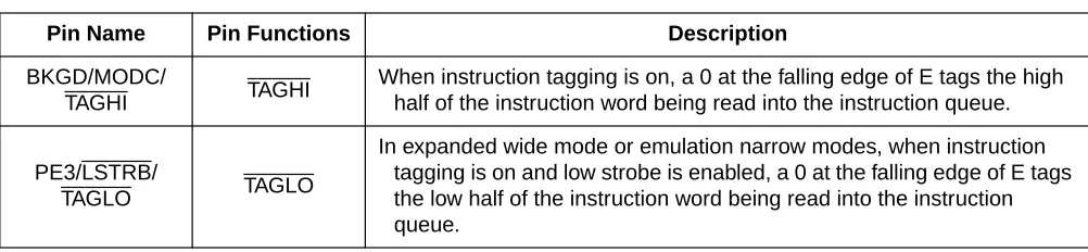
[image:15.612.55.556.176.292.2]The tag pins inTable 2-1 (part of the MEBI) may also be a part of the breakpoint operation.
Table 2-1 External System Pins Associated With DBG and MEBI
Pin Name Pin Functions Description
BKGD/MODC/
TAGHI TAGHI
When instruction tagging is on, a 0 at the falling edge of E tags the high half of the instruction word being read into the instruction queue.
PE3/LSTRB/
TAGLO TAGLO
PRINTED VERSIONS ARE UNCONTROLLED EXCEPT WHEN STAMPED "CONTROLLED COPY" IN RED
Block Guide — S12DBG V1
"CONTROLLED COPY"
IN RED
Section 3 Memory Map/Register Definition
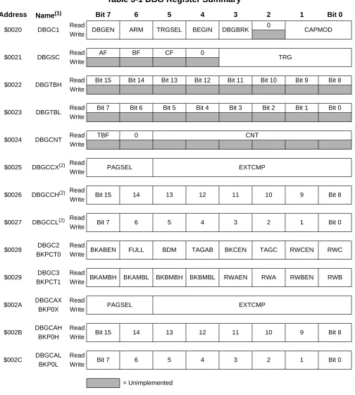
[image:17.612.59.563.147.707.2]A summary of the registers associated with the DBG sub-block is shown inTable 3-1. Detailed descriptions of the registers and bits are given in the subsections that follow.
Table 3-1 DBG Register Summary
Address Name(1) Bit 7 6 5 4 3 2 1 Bit 0
$0020 DBGC1 Read DBGEN ARM TRGSEL BEGIN DBGBRK 0 CAPMOD Write
$0021 DBGSC Read AF BF CF 0 TRG
Write
$0022 DBGTBH Read Bit 15 Bit 14 Bit 13 Bit 12 Bit 11 Bit 10 Bit 9 Bit 8 Write
$0023 DBGTBL Read Bit 7 Bit 6 Bit 5 Bit 4 Bit 3 Bit 2 Bit 1 Bit 0 Write
$0024 DBGCNT Read TBF 0 CNT
Write
$0025 DBGCCX(2) Read PAGSEL EXTCMP
Write
$0026 DBGCCH(2) Read Bit 15 14 13 12 11 10 9 Bit 8
Write
$0027 DBGCCL(2) Read Bit 7 6 5 4 3 2 1 Bit 0
Write
$0028 DBGC2 Read BKABEN FULL BDM TAGAB BKCEN TAGC RWCEN RWC BKPCT0 Write
$0029 DBGC3 Read BKAMBH BKAMBL BKBMBH BKBMBL RWAEN RWA RWBEN RWB BKPCT1 Write
$002A DBGCAX Read PAGSEL EXTCMP
PRINTED VERSIONS ARE UNCONTROLLED EXCEPT WHEN STAMPED
"CONTROLLED COPY"
IN RED
Block Guide — S12DBG V1
3.1 Register Descriptions
This section consists of the DBG register descriptions in address order. Most of the register bits can be written to in either BKP or DBG mode, although they may not have any effect in one of the modes. However, the only bits in the DBG module that can be written while the debugger is armed (ARM = 1) are DBGEN and ARM
3.1.1 Debug Control Register 1 (DBGC1)
[image:18.612.62.560.54.221.2]NOTE: All bits are used in DBG mode only.
Figure 3-1 Debug Control Register (DBGC1)
NOTE: This register cannot be written if BKP mode is enabled (BKABEN in DBGC2 is set).
$002D DBGCBX Read PAGSEL EXTCMP
BKP1X Write
$002E DBGCBH Read Bit 15 14 13 12 11 10 9 Bit 8
BKP1H Write
$002F DBGCBL Read Bit 7 6 5 4 3 2 1 Bit 0
BKP1L Write
NOTES:
1. The DBG module is designed for backwards compatibility to existing BKP modules. Register and bit names have changed from the BKP module. This column shows the DBG register name, as well as the BKP register name for reference. 2. Comparator C can be used to enhance the BKP mode, by providing a third breakpoint.
Register address $0020
7 6 5 4 3 2 1 0
R
DBGEN ARM TRGSEL BEGIN DBGBRK 0 CAPMOD
W
Reset: 0 0 0 0 0 0 0 0
[image:18.612.92.525.461.542.2]= Unimplemented or Reserved
Table 3-1 DBG Register Summary (Continued)
Address Name(1) Bit 7 6 5 4 3 2 1 Bit 0
"CONTROLLED COPY"
IN RED
DBGEN — DBG Mode Enable Bit
The DBGEN bit enables the DBG module for use in DBG mode. This bit cannot be set if the MCU is in secure mode.
1 = DBG mode enabled 0 = DBG mode disabled
ARM — Arm Bit
The ARM bit controls whether the debugger is comparing and storing data in the Trace Buffer. See
4.2.4 Arming the DBG Module for more information.
1 = Debugger armed 0 = Debugger unarmed
NOTE: This bit cannot be set if the DBGEN bit is not also being set at the same time. For example, a write of 01 to DBGEN[7:6] will be interpreted as a write of 00.
TRGSEL — Trigger Selection Bit
The TRGSEL bit controls the triggering condition for comparators A and B in DBG mode. It serves essentially the same function as the TAGAB bit in the DBGC2 register does in BKP mode. See4.2.1.2 Trigger Selectionfor more information. TRGSEL may also determine the type of breakpoint based on comparator A and B if enabled in DBG mode (DBGBRK = 1). Please refer to 4.3.1 Breakpoint
Based on Comparator A and B.
1 = Trigger before opcode at compare address gets executed (tagged-type) 0 = Trigger on any compare address match
BEGIN — Begin/End Trigger Bit
The BEGIN bit controls whether the trigger begins or ends storing of data in the Trace Buffer. See
4.2.8.1 Storing with Begin-Trigger and 4.2.8.2 Storing with End-Trigger for more details.
1 = Trigger before storing data 0 = Trigger at end of stored data
DBGBRK — DBG Breakpoint Enable Bit
The DBGBRK bit controls whether the debugger will request a breakpoint based on comparator A and B to the CPU upon completion of a tracing session. Please refer to 4.3 Breakpoints for further details.
PRINTED VERSIONS ARE UNCONTROLLED EXCEPT WHEN STAMPED
"CONTROLLED COPY"
IN RED
Block Guide — S12DBG V1
CAPMOD — Capture Mode Field
SeeTable 3-2 for capture mode field definitions. In LOOP1 mode, the debugger will automatically inhibit redundant entries into capture memory. In DETAIL mode, the debugger is storing address and data for all cycles except program fetch (P) and free (f) cycles. In PROFILE mode, the debugger is returning the address of the last instruction executed by the CPU on each access of trace buffer address. Refer to 4.2.6 Capture Modes for more information.
[image:20.612.90.526.318.401.2]3.1.2 Debug Status and Control Register (DBGSC)
Figure 3-2 Debug Status and Control Register (DBGSC)
AF — Trigger A Match Flag
The AF bit indicates if Trigger A match condition was met since arming. This bit is cleared when ARM in DBGC1 is written to a one or on any write to this register.
1 = Trigger A match
0 = Trigger A did not match
BF — Trigger B Match Flag
The BF bit indicates if Trigger B match condition was met since arming.This bit is cleared when ARM in DBGC1 is written to a one or on any write to this register.
1 = Trigger B match
0 = Trigger B did not match
CF — Comparator C Match Flag
The CF bit indicates if Comparator C match condition was met since arming.This bit is cleared when ARM in DBGC1 is written to a one or on any write to this register.
1 = Comparator C match
0 = Comparator C did not match
Table 3-2 CAPMOD Encoding
CAPMOD Description
00 Normal
01 LOOP1
10 DETAIL
11 PROFILE
Register address $0021
7 6 5 4 3 2 1 0
R AF BF CF 0
TRG W
Reset: 0 0 0 0 0 0 0 0
"CONTROLLED COPY"
IN RED
TRG — Trigger Mode Bits
The TRG bits select the trigger mode of the DBG module as shownTable 3-3. See 4.2.5 Trigger
Modes for more detail.
3.1.3 Debug Trace Buffer Register (DBGTB)
Figure 3-3 Debug Trace Buffer Register (DBGTB)
Bits 15:0 — Trace Buffer Data Bits
[image:21.612.184.426.113.325.2]The Trace Buffer data bits contain the data of the Trace Buffer. This register can be read only as a word read. Any byte reads or misaligned access of these registers will return 0 and will not cause the trace buffer pointer to increment to the next trace buffer address. The same is true for word reads while the debugger is armed. In addition, this register may appear to contain incorrect data if it is not read with
Table 3-3 Trigger Mode Encoding
TRG Value Meaning
0000 A only
0001 A or B
0010 A then B
0011 Event only B
0100 A then event only B
0101 A and B (full mode)
0110 A and Not B (full mode)
0111 Inside range
1000 Outside range
1001 ↓ 1111
Reserved (Defaults to A only)
Register address $0022-3
15 14 13 12 11 10 9 8 7 6 5 4 3 2 1 0
R Bit 15 Bit 14 Bit 13 Bit 12 Bit 11 Bit 10 Bit 9 Bit 8 Bit 7 Bit 6 Bit 5 Bit 4 Bit 3 Bit 2 Bit 1 Bit 0 W
Reset: 0 0 0 0 0 0 0 0 0 0 0 0 0 0 0 0
PRINTED VERSIONS ARE UNCONTROLLED EXCEPT WHEN STAMPED
"CONTROLLED COPY"
IN RED
Block Guide — S12DBG V1
[image:22.612.94.522.101.186.2]3.1.4 Debug Count Register (DBGCNT)
Figure 3-4 Debug Count Register (DBCNT)
TBF — Trace Buffer Full
The TBF bit indicates that the trace buffer has stored 64 or more words of data since it was last armed. If this bit is set, then all 64 words will be valid data, regardless of the value in CNT[5:0]. The TBF bit is cleared when ARM in DBGC1 is written to a one.
CNT — Count Value
The CNT bits indicate the number of valid data words stored in the Trace Buffer.Table 3-4 shows the correlation between the CNT bits and the number of valid data words in the Trace Buffer. When the CNT rolls over to zero, the TBF bit will be set and incrementing of CNT will continue if DBG is in end-trigger mode. The DBGCNT register is cleared when ARM in DBGC1 is written to a one.
Register address $0024
7 6 5 4 3 2 1 0
R TBF 0 CNT
W
Reset: 0 0 0 0 0 0 0 0
= Unimplemented or Reserved
Table 3-4 CNT Decoding Table
TBF CNT Description
0 000000 No data valid
0 000001 1 word valid
0
000010 .. .. 111110
2 words valid .. .. 62 words valid
0 111111 63 words valid
1 000000
64 words valid; if BEGIN = 1, the ARM bit will be cleared. A breakpoint will be generated if
DBGBRK = 1
1
000001 .. .. 111111
[image:22.612.172.444.390.613.2]"CONTROLLED COPY"
IN RED
[image:23.612.93.525.89.152.2]3.1.5 Debug Comparator C Extended Register (DBGCCX)
Figure 3-5 Debug Comparator C Extended Register (DBGCCX)
PAGSEL — Page Selector Field
In both BKP and DBG mode, PAGSEL selects the type of paging as shown inTable 3-5.
DPAGE and EPAGE are not yet implemented so the value in bit 7 will be ignored (i.e., PAGSEL values of 10 and 11 will be interpreted as values of 00 and 01, respectively).
EXTCMP — Comparator C Extended Compare Bits
The EXTCMP bits are used as comparison address bits as shown inTable 3-5 along with the appropriate PPAGE, DPAGE, or EPAGE signal from the core.
NOTE: Comparator C can be used when the DBG module is configured for BKP mode. Extended addressing comparisons for Comparator C use PAGSEL and will operate differently to the way that Comparator A and B operates in BKP mode.
Register address $0025
7 6 5 4 3 2 1 0
R
PAGSEL EXTCMP
W
Reset: 0 0 0 0 0 0 0 0
Table 3-5 PAGSEL Decoding(1)
NOTES:
1. SeeFigure 3-6.
PAGSEL Description EXTCMP Comment
00 Normal (64k) Not used No paged memory
01 PPAGE
(256 — 16K pages)
EXTCMP[5:0] is compared to
address bits [21:16](2)
2. Current HCS12 implementations have PPAGE limited to 6 bits. Therefore, EXTCMP[5:4] should be set to 00.
PPAGE[7:0] / XAB[21:14] becomes
address bits [21:14](1)
10(3)
3. Data Page (DPAGE) and Extra Page (EPAGE) are reserved for implementation on devices that support paged data and extra space.
DPAGE (reserved) (256 — 4K pages)
EXTCMP[3:0] is compared to address bits [19:16]
DPAGE / XAB[21:14] becomes address bits [19:12]
PRINTED VERSIONS ARE UNCONTROLLED EXCEPT WHEN STAMPED
"CONTROLLED COPY"
IN RED
Block Guide — S12DBG V1
3.1.6 Debug Comparator C Register (DBGCC)
Figure 3-7 Debug Comparator C Register (DBGCC)
Bits 15:0 — Comparator C Compare Bits
The Comparator C compare bits control whether Comparator C will compare the address bus bits [15:0] to a logic one or logic zero. SeeTable 3-6.
1 = Compare corresponding address bit to a logic one 0 = Compare corresponding address bit to a logic zero
NOTE: This register will be cleared automatically when the DBG module is armed in LOOP1 mode.
DBGCXX DBGCXH[15:12]
PAGSEL EXTCMP
BIT 15 BIT 14 BIT 13 BIT 12
7 6 0
5
0
4 3 2 1 BIT 0
SEE NOTE 1
PORTK/XAB XAB21 XAB20 XAB19 XAB18 XAB17 XAB16 XAB15 XAB14
PPAGE PIX7 PIX6 PIX5 PIX4 PIX3 PIX2 PIX1 PIX0
SEE NOTE 2 NOTES:
1. In BKP and DBG mode, PAGSEL selects the type of paging as shown inTable 3-5.
[image:24.612.55.551.61.239.2]2. Current HCS12 implementations are limited to six PPAGE bits, PIX[5:0]. Therefore, EXTCMP[5:4] = 00.
Figure 3-6 Comparator C Extended Comparison in BKP/DBG Mode
Register address $0026-7
15 14 13 12 11 10 9 8 7 6 5 4 3 2 1 0
R Bit 15 Bit 14 Bit 13 Bit 12 Bit 11 Bit 10 Bit 9 Bit 8 Bit 7 Bit 6 Bit 5 Bit 4 Bit 3 Bit 2 Bit 1 Bit 0 W
Reset: 0 0 0 0 0 0 0 0 0 0 0 0 0 0 0 0
= Unimplemented or Reserved
Table 3-6 Comparator C Compares
PAGSEL EXTCMP Compare High-Byte Compare
x0 No compare DBGCCH[7:0] = AB[15:8]
x1 EXTCMP[5:0] = XAB[21:16] DBGCCH[7:0] = XAB[15:14],AB[13:8]
"CONTROLLED COPY"
IN RED
[image:25.612.95.526.89.152.2]3.1.7 Debug Control Register 2 (DBGC2)
Figure 3-8 Debug Control Register 2 (DBGC2)
BKABEN — Breakpoint Using Comparator A and B Enable
This bit enables the breakpoint capability using comparator A and B, when set (BKP mode) the DBGEN bit in DBGC1 cannot be set.
1 = Breakpoint module on 0 = Breakpoint module off
FULL — Full Breakpoint Mode Enable
This bit controls whether the breakpoint module is in Dual Mode or Full Mode. In Full Mode comparator A is used to match address and comparator B is used to match data. See 4.1.2 Full
Breakpoint Mode for more details.
1 = Full Breakpoint Mode enabled 0 = Dual Address Mode enabled
BDM — Background Debug Mode Enable
This bit determines if the breakpoint causes the system to enter Background Debug Mode (BDM) or initiate a Software Interrupt (SWI).
1 = Go to BDM on a break request
0 = Go to Software Interrupt on a break request
TAGAB — Comparator A/B Tag Select
This bit controls whether the breakpoint will cause a break on the next instruction boundary (force) or on a match that will be an executable opcode (tagged). Non-executed opcodes cannot cause a tagged breakpoint.
1 = On match, break if/when the instruction is about to be executed (tagged)
Register address $0028
7 6 5 4 3 2 1 0
R
BKABEN(1)
NOTES:
1. When BKABEN is set (BKP mode), all bits in DBGC2 are available. When BKABEN is cleared and DBG is used in DBG mode, bits FULL and TAGAB have no meaning.
FULL BDM TAGAB BKCEN(2)
2. These bits can be used in BKP mode and DBG mode (when capture mode is not set in LOOP1) to pro-vide a third breakpoint.
TAGC(2) RWCEN(2) RWC(2) W
PRINTED VERSIONS ARE UNCONTROLLED EXCEPT WHEN STAMPED
"CONTROLLED COPY"
IN RED
Block Guide — S12DBG V1
BKCEN — Breakpoint Comparator C Enable Bit
This bit enables the breakpoint capability using comparator C. 1 = Comparator C enabled for breakpoint
0 = Comparator C disabled for breakpoint
NOTE: This bit will be cleared automatically when the DBG module is armed in LOOP1 mode.
TAGC — Comparator C Tag Select
This bit controls whether the breakpoint will cause a break on the next instruction boundary (force) or on a match that will be an executable opcode (tagged). Non-executed opcodes cannot cause a tagged breakpoint.
1 = On match, break if/when the instruction is about to be executed (tagged) 0 = On match, break at the next instruction boundary (force)
RWCEN — Read/Write Comparator C Enable Bit
The RWCEN bit controls whether read or write comparison is enabled for Comparator C. RWCEN is not useful for tagged breakpoints.
1 = Read/Write is used in comparison 0 = Read/Write is not used in comparison
RWC — Read/Write Comparator C Value Bit
The RWC bit controls whether read or write is used in compare for Comparator C. The RWC bit is not used if RWCEN = 0.
1 = Read cycle will be matched 0 = Write cycle will be matched
[image:26.612.98.530.475.532.2]3.1.8 Debug Control Register 3 (DBGC3)
Figure 3-9 Debug Control Register 3 (DBGC3)
BKAMBH:BKAMBL — Breakpoint Mask High Byte and Low Byte for First Address
In Dual or Full Mode, these bits may be used to mask (disable) the comparison of the high and/or low bytes of the first address breakpoint. The functionality is as given inTable 3-7.
Register address $0029
7 6 5 4 3 2 1 0
R
BKAMBH(1)
NOTES:
1. In DBG mode, BKAMBH:BKAMBL has no meaning and are forced to zero’s. BKAMBL(1) BKBMBH(2)
2. In DBG mode, BKBMBH:BKBMBL are used in full mode to qualify data.
BKBMBL(2) RWAEN RWA RWBEN RWB W
"CONTROLLED COPY"
IN RED
The x:0 case is for a Full Address Compare. When a program page is selected, the full address compare will be based on bits for a 20-bit compare. The registers used for the compare are {DBGCAX[5:0], DBGCAH[5:0], DBGCAL[7:0]}, where DBGAX[5:0] corresponds to PPAGE[5:0] or extended address bits [19:14] and CPU address [13:0]. When a program page is not selected, the full address compare will be based on bits for a 16-bit compare. The registers used for the compare are
{DBGCAH[7:0], DBGCAL[7:0]} which corresponds to CPU address [15:0].
NOTE: This extended address compare scheme causes an aliasing problem in BKP mode in which several physical addresses may match with a single logical address. This problem may be avoided by using DBG mode to generate breakpoints.
The 1:0 case is not sensible because it would ignore the high order address and compare the low order and expansion addresses. Logic forces this case to compare all address lines (effectively ignoring the BKAMBH control bit).
The 1:1 case is useful for triggering a breakpoint on any access to a particular expansion page. This only makes sense if a program page is being accessed so that the breakpoint trigger will occur only if DBGCAX compares.
BKBMBH:BKBMBL — Breakpoint Mask High Byte and Low Byte of Data (Second Address)
[image:27.612.85.530.73.175.2]In Dual Mode, these bits may be used to mask (disable) the comparison of the high and/or low bytes of the second address breakpoint. The functionality is as given inTable 3-8.
Table 3-7 Breakpoint Mask Bits for First Address
BKAMBH:BKAMBL Address Compare DBGCAX DBGCAH DBGCAL
x:0 Full address compare Yes(1)
NOTES:
1. If PPAGE is selected.
Yes Yes
0:1 256 byte address range Yes(1) Yes No
1:1 16K byte address range Yes(1) No No
Table 3-8 Breakpoint Mask Bits for Second Address (Dual Mode)
BKBMBH:BKBMBL Address Compare DBGCBX DBGCBH DBGCBL
x:0 Full address compare Yes(1) Yes Yes
PRINTED VERSIONS ARE UNCONTROLLED EXCEPT WHEN STAMPED
"CONTROLLED COPY"
IN RED
Block Guide — S12DBG V1
The x:0 case is for a Full Address Compare. When a program page is selected, the full address compare will be based on bits for a 20-bit compare. The registers used for the compare are {DBGCBX[5:0], DBGCBH[5:0], DBGCBL[7:0]} where DBGCBX[5:0] corresponds to PPAGE[5:0] or extended address bits [19:14] and CPU address [13:0]. When a program page is not selected, the full address compare will be based on bits for a 16-bit compare. The registers used for the compare are
{DBGCBH[7:0], DBGCBL[7:0]} which corresponds to CPU address [15:0].
NOTE: This extended address compare scheme causes an aliasing problem in BKP mode in which several physical addresses may match with a single logical address. This problem may be avoided by using DBG mode to generate breakpoints.
The 1:0 case is not sensible because it would ignore the high order address and compare the low order and expansion addresses. Logic forces this case to compare all address lines (effectively ignoring the BKBMBH control bit).
The 1:1 case is useful for triggering a breakpoint on any access to a particular expansion page. This only makes sense if a program page is being accessed so that the breakpoint trigger will occur only if DBGCBX compares.
In Full Mode, these bits may be used to mask (disable) the comparison of the high and/or low bytes of the data breakpoint. The functionality is as given inTable 3-9.
RWAEN — Read/Write Comparator A Enable Bit
The RWAEN bit controls whether read or write comparison is enabled for Comparator A. See
4.2.1.1 Read or Write Comparison for more information. This bit is not useful for tagged operations.
1 = Read/Write is used in comparison 0 = Read/Write is not used in comparison
RWA — Read/Write Comparator A Value Bit
The RWA bit controls whether read or write is used in compare for Comparator A. The RWA bit is not used if RWAEN = 0.
[image:28.612.85.531.354.468.2]1 = Read cycle will be matched 0 = Write cycle will be matched
Table 3-9 Breakpoint Mask Bits for Data Breakpoints (Full Mode)
BKBMBH:BKBMBL Data Compare DBGCBX DBGCBH DBGCBL
0:0 High and low byte
compare No(1)
NOTES:
1. Expansion addresses for breakpoint B are not applicable in this mode.
Yes Yes
0:1 High byte No(1) Yes No
1:0 Low byte No(1) No Yes
"CONTROLLED COPY"
IN RED
RWBEN — Read/Write Comparator B Enable Bit
The RWBEN bit controls whether read or write comparison is enabled for Comparator B. See
4.2.1.1 Read or Write Comparison for more information. This bit is not useful for tagged operations.
1 = Read/Write is used in comparison 0 = Read/Write is not used in comparison
RWB — Read/Write Comparator B Value Bit
The RWB bit controls whether read or write is used in compare for Comparator B. The RWB bit is not used if RWBEN = 0.
1 = Read cycle will be matched 0 = Write cycle will be matched
NOTE: RWB and RWBEN are not used in Full Mode.
[image:29.612.95.526.290.346.2]3.1.9 Debug Comparator A Extended Register (DBGCAX)
Figure 3-10 Debug Comparator A Extended Register (DBGCAX)
PAGSEL — Page Selector Field
If DBGEN is set in DBGC1, then PAGSEL selects the type of paging as shown inTable 3-10. DPAGE and EPAGE are not yet implemented so the value in bit 7 will be ignored (i.e., PAGSEL values of 10 and 11 will be interpreted as values of 00 and 01, respectively).
In BKP mode, PAGSEL has no meaning and EXTCMP[5:0] are compared to address bits [19:14] if the address is in the FLASH/ROM memory space.
EXTCMP — Comparator A Extended Compare Bits
The EXTCMP bits are used as comparison address bits as shown inTable 3-10 along with the appropriate PPAGE, DPAGE, or EPAGE signal from the core.
Register address $002A
7 6 5 4 3 2 1 0
R
PAGSEL EXTCMP
W
PRINTED VERSIONS ARE UNCONTROLLED EXCEPT WHEN STAMPED
"CONTROLLED COPY"
IN RED
Block Guide — S12DBG V1
3.1.10 Debug Comparator A Register (DBGCA)
Figure 3-12 Debug Comparator A Register (DBGCA)
Bits 15:0 — Comparator A Compare Bits
The Comparator A compare bits control whether Comparator A compares the address bus bits [15:0] to a logic one or logic zero. SeeTable 3-10.
[image:30.612.67.544.74.190.2]1 = Compare corresponding address bit to a logic one 0 = Compare corresponding address bit to a logic zero
Table 3-10 Comparator A or B Compares
Mode EXTCMP Compare High-Byte Compare
BKP(1)
NOTES:
1. SeeFigure 3-11.
Not FLASH/Rom access No compare DBGCxH[7:0] = AB[15:8]
FLASH/Rom access EXTCMP[5:0] = XAB[19:14] DBGCxH[5:0] = AB[13:8]
DBG(2)
2. SeeFigure 3-6(note that while this figure provides extended comparisons for comparator C, the figure also pertains to comparators A and B in DBG mode only).
PAGSEL = 00 No compare DBGCxH[7:0] = AB[15:8]
PAGSEL = 01 EXTCMP[5:0] = XAB[21:16] DBGCxH[7:0] = XAB[15:14], AB[13:8]
PAGSEL EXTCMP
DBGCXX 0 0 5 4 3 2 1 BIT 0
SEE NOTE 1
PORTK/XAB XAB21 XAB20 XAB19 XAB18 XAB17 XAB16 XAB15 XAB14
PPAGE PIX7 PIX6 PIX5 PIX4 PIX3 PIX2 PIX1 PIX0
SEE NOTE 2 NOTES:
[image:30.612.124.492.237.392.2]1. In BKP mode, PAGSEL has no functionality. Therefore, set PAGSEL to 00 (reset state). 2. Current HCS12 implementations are limited to six PPAGE bits, PIX[5:0].
Figure 3-11 Comparators A and B Extended Comparison in BKP Mode
Register address $002B-C
15 14 13 12 11 10 9 8 7 6 5 4 3 2 1 0
R
Bit 15 Bit 14 Bit 13 Bit 12 Bit 11 Bit 10 Bit 9 Bit 8 Bit 7 Bit 6 Bit 5 Bit 4 Bit 3 Bit 2 Bit 1 Bit 0 W
Reset: 0 0 0 0 0 0 0 0 0 0 0 0 0 0 0 0
"CONTROLLED COPY"
IN RED
[image:31.612.92.526.90.151.2]3.1.11 Debug Comparator B Extended Register (DBGCBX)
Figure 3-13 Debug Comparator B Extended Register (DBGCBX)
PAGSEL — Page Selector Field
If DBGEN is set in DBGC1, then PAGSEL selects the type of paging as shown inTable 3-5. DPAGE and EPAGE are not yet implemented so the value in bit 7 will be ignored (i.e., PAGSEL values of 10 and 11 will be interpreted as values of 00 and 01, respectively.)
In BKP mode, PAGSEL has no meaning and EXTCMP[5:0] are compared to address bits [19:14] if the address is in the FLASH/ROM memory space.
EXTCMP — Comparator B Extended Compare Bits
The EXTCMP bits are used as comparison address bits as shown inTable 3-5 along with the appropriate PPAGE, DPAGE, or EPAGE signal from the core. Also seeTable 3-10.
3.1.12 Debug Comparator B Register (DBGCB)
Figure 3-14 Debug Comparator B Register (DBGCB)
Bits 15:0 — Comparator B High Compare Bits
The Comparator B compare bits control whether Comparator B compares the address bus bits [15:0] or data bus bits [15:0] to a logic one or logic zero. SeeTable 3-10.
1 = Compare corresponding address bit to a logic one, compares to data if in Full mode 0 = Compare corresponding address bit to a logic zero, compares to data if in Full mode
Register address $002D
7 6 5 4 3 2 1 0
R
PAGSEL EXTCMP
W
Reset: 0 0 0 0 0 0 0 0
Register address $002E-F
15 14 13 12 11 10 9 8 7 6 5 4 3 2 1 0
R
Bit 15 Bit 14 Bit 13 Bit 12 Bit 11 Bit 10 Bit 9 Bit 8 Bit 7 Bit 6 Bit 5 Bit 4 Bit 3 Bit 2 Bit 1 Bit 0 W
PRINTED VERSIONS ARE UNCONTROLLED EXCEPT WHEN STAMPED "CONTROLLED COPY" IN RED
Block Guide — S12DBG V1
"CONTROLLED COPY"
IN RED
Section 4 Functional Description
This section provides a complete functional description of the DBG module. The DBG module can be configured to run in either of two modes, BKP or DBG. BKP mode is enabled by setting BKABEN in DBGC2. DBG mode is enabled by setting DBGEN in DBGC1. Setting BKABEN in DBGC2 overrides the DBGEN in DBGC1 and prevents DBG mode. If the part is in secure mode, DBG mode cannot be enabled.
4.1 DBG Operating in BKP Mode
In BKP mode, the DBG will be fully backwards compatible with the existing BKP_ST12_A module. The DBGC2 register has four additional bits that were not available on existing BKP_ST12_A modules. As long as these bits are written to either all ones or all zeros, they should be transparent to the user. All ones would enable Comparator C to be used as a breakpoint, but tagging would be enabled. The match address register would be all zeros if not modified by the user. Therefore, code executing at address $0000 would have to occur before a breakpoint based on Comparator C would happen.
The DBG module in BKP mode supports two modes of operation: Dual Address Mode and Full Breakpoint Mode. Within each of these modes, forced or tagged breakpoint types can be used. Forced breakpoints occur at the next instruction boundary if a match occurs and tagged breakpoints allow for breaking just before the tagged instruction executes. The action taken upon a successful match can be to either place the CPU in Background Debug Mode or to initiate a software interrupt.
The Breakpoint can operate in Dual Address Mode or Full Breakpoint Mode. Each of these modes is discussed in the subsections below.
4.1.1 Dual Address Mode
When Dual Address Mode is enabled, two address breakpoints can be set. Each breakpoint can cause the system to enter Background Debug Mode or to initiate a software interrupt based upon the state of BDM in DBGC2 being logic one or logic zero, respectively. BDM requests have a higher priority than SWI requests. No data breakpoints are allowed in this mode.
PRINTED VERSIONS ARE UNCONTROLLED EXCEPT WHEN STAMPED
"CONTROLLED COPY"
IN RED
Block Guide — S12DBG V1
TAGAB in DBGC2 selects whether the breakpoint mode is forced or tagged. When TAGAB is set in DBGC2, only addresses are compared and data is ignored. The BKAMBH:L bits in DBGC3 select whether or not the breakpoint is matched exactly, is a range breakpoint, or is in page space. The
BKBMBH:L bits in DBGC3 select whether the data is matched on the high byte, low byte, or both bytes. RWA and RWAEN bits in DBGC2 select whether the type of bus cycle to match is a read or a write when performing forced breakpoints. RWB and RWBEN bits in DBGC2 are not used in Full Breakpoint Mode.
NOTE: The full trigger mode is designed to be used for either a word access or a byte access, but not both at the same time. Confusing trigger operation (seemingly false triggers or no trigger) can occur if the trigger address occurs in the user program as both byte and word accesses.
4.1.3 Breakpoint Priority
Breakpoint operation is first determined by the state of the BDM module. If the BDM module is already active, meaning the CPU is executing out of BDM firmware, Breakpoints are not allowed. In addition, while executing a BDM TRACE command, tagging into BDM is not allowed. If BDM is not active, the Breakpoint will give priority to BDM requests over SWI requests. This condition applies to both forced and tagged breakpoints.
In all cases, BDM related breakpoints will have priority over those generated by the Breakpoint sub-block. This priority includes breakpoints enabled by the TAGLO and TAGHI external pins of the system that interface with the BDM directly and whose signal information passes through and is used by the Breakpoint sub-block.
NOTE: BDM should not be entered from a breakpoint unless the ENABLE bit is set in the BDM. Even if the ENABLE bit in the BDM is cleared, the CPU actually executes the BDM firmware code. It checks the ENABLE and returns if ENABLE is not set. If the BDM is not serviced by the monitor then the breakpoint would be re-asserted when the BDM returns to normal CPU flow.
There is no hardware to enforce restriction of breakpoint operation if the BDM is not enabled.
"CONTROLLED COPY"
IN RED
4.1.4 Using Comparator C in BKP Mode
The original BKP_ST12_A module supports two breakpoints. The DBG_ST12_A module can be used in BKP mode and allow a third breakpoint using Comparator C. Four additional bits, BKCEN, TAGC, RWCEN, and RWC in DBGC2 in conjunction with additional Comparator C address registers, DBGCCX, DBGCCH, and DBGCCL allow the user to set up a third breakpoint. Using PAGSEL in DBGCCX for expanded memory will work differently than the way paged memory is done using Comparator A and B in BKP mode. See 3.1.5 Debug Comparator C Extended Register (DBGCCX) for more information on using Comparator C.
4.2 DBG Operating in DBG Mode
Enabling the DBG module in DBG mode, allows the arming, triggering, and storing of data in the Trace Buffer and can be used to cause CPU breakpoints. The DBG module is made up of three main blocks, the Comparators, Trace Buffer Control Logic, and the Trace Buffer.
NOTE: In general, there is a latency between the triggering event appearing on the bus and being detected by the DBG circuitry. In general, tagged triggers will be more predictable than forced triggers.
4.2.1 Comparators
The DBG contains three comparators, A, B, and C. Comparator A compares the core address bus with the address stored in DBGCAH and DBGCAL. Comparator B compares the core address bus with the address stored in DBGCBH and DBGCBL except in full mode, where it compares the data buses to the data stored in DBGCBH and DBGCBL. Comparator C can be used as a breakpoint generator or as the address comparison unit in the LOOP1 mode. Matches on Comparator A, B, and C are signaled to the Trace Buffer Control (TBC) block. When PAGSEL = 01, registers DBGCAX, DBGCBX, and DBGCCX are used to match the upper addresses as shown inTable 3-5.
NOTE: If a tagged-type C breakpoint is set at the same address as an A/B tagged-type trigger (including the initial entry in an inside or outside range trigger), the C breakpoint will have priority and the trigger will not be recognized.
4.2.1.1 Read or Write Comparison
PRINTED VERSIONS ARE UNCONTROLLED EXCEPT WHEN STAMPED
"CONTROLLED COPY"
IN RED
Block Guide — S12DBG V1
4.2.1.2 Trigger Selection
The TRGSEL bit in DBGC1 is used to determine the triggering condition in DBG mode. TRGSEL applies to both trigger A and B except in the event only trigger modes. By setting TRGSEL, the Comparators A and B will qualify a match with the output of opcode tracking logic and a trigger occurs before the tagged instruction executes (tagged-type trigger). With the TRGSEL bit cleared, a comparator match forces a trigger when the matching condition occurs (force-type trigger).
NOTE: If the TRGSEL is set, the address stored in the comparator match address registers must be an opcode address for the trigger to occur.
4.2.2 Trace Buffer Control (TBC)
The TBC is the main controller for the DBG module. Its function is to decide whether data should be stored in the Trace Buffer based on the trigger mode and the match signals from the comparator. The TBC also determines whether a request to break the CPU should occur.
4.2.3 Begin- and End-Trigger
The definitions of begin- and end-trigger as used in the DBG module are as follows:
• Begin-trigger: Storage in Trace Buffer occurs after the trigger and continues until 64 locations are filled.
• End-trigger: Storage in Trace Buffer occurs until the trigger, with the least recent data falling out of the Trace Buffer if more than 64 words are collected.
4.2.4 Arming the DBG Module
[image:36.612.103.505.69.188.2]In DBG mode, arming occurs by setting DBGEN and ARM in DBGC1. The ARM bit in DBGC1 is cleared when the trigger condition is met in end-trigger mode or when the Trace Buffer is filled in begin-trigger mode. The TBC logic determines whether a trigger condition has been met based on the trigger mode and the trigger selection.
Table 4-1 Read or Write Comparison Logic Table
RWAEN bit RWA bit RW signal Comment
0 x 0 Write Data Bus
0 x 1 Read Data Bus
1 0 0 Write Data Bus
1 0 1 No Data bus compare since RW=1
1 1 0 No Data bus compare since RW=0
"CONTROLLED COPY"
IN RED
4.2.5 Trigger Modes
The DBG module supports nine trigger modes. The trigger modes are encoded as shown inTable 3-3. The trigger mode is used as a qualifier for either starting or ending the storing of data in the Trace Buffer. When the match condition is met, the appropriate flag A or B is set in DBGSC. Arming the DBG module clears the A, B, and C flags in DBGSC. In all trigger modes except for the event-only modes and DETAIL capture mode change of flow addresses are stored in the Trace Buffer. In the event-only modes only the value on the data bus at the trigger event B will be stored. In DETAIL capture mode address and data for all cycles except program fetch (P) and free (f) cycles are stored in trace buffer.
4.2.5.1 A Only
In the A only trigger mode, if the match condition for A is met, the A flag in DBGSC is set and a trigger occurs.
4.2.5.2 A or B
In the A or B trigger mode, if the match condition for A or B is met, the corresponding flag in DBGSC is set and a trigger occurs.
4.2.5.3 A then B
In the A then B trigger mode, the match condition for A must be met before the match condition for B is compared. When the match condition for A or B is met, the corresponding flag in DBGSC is set. The trigger occurs only after A then B have matched.
NOTE: When Tagging and using A then B, if addresses A and B are close together, then B may not complete the trigger sequence. This occurs when A and B are in the instruction queue at the same time. Basically the A trigger has not yet occurred, so the B instruction is not tagged. Generally, if address B is at least six addresses higher than address A (or B is lower than A) and there are not changes of flow to put these in the queue at the same time, then this operation should trigger properly.
4.2.5.4 Event-Only B (Store Data)
In the Event-Only B trigger mode, if the match condition for B is met, the B flag in DBGSC is set and a trigger occurs. The Event-Only B trigger mode is considered a begin-trigger type and the BEGIN bit in DBGC1 is ignored. Event-Only B is incompatible with instruction tagging (TRGSEL = 1), and thus the value of TRGSEL is ignored. Please refer to 4.2.7 Storage Memory for more information.
PRINTED VERSIONS ARE UNCONTROLLED EXCEPT WHEN STAMPED
"CONTROLLED COPY"
IN RED
Block Guide — S12DBG V1
trigger mode is considered a begin-trigger type and BEGIN in DBGC1 is ignored. TRGSEL in DBGC1 applies only to the match condition for A. Please refer to 4.2.7 Storage Memory for more information.
This trigger mode is incompatible with the Detail Capture mode so the Detail Capture mode will have priority. TRGSEL and BEGIN will not be ignored and this trigger mode will be the same as A then B.
4.2.5.6 A and B (Full Mode)
In the A and B trigger mode, Comparator A compares to the address bus and Comparator B compares to the data bus. In the A and B trigger mode, if the match condition for A and B happen on the same bus cycle, both the A and B flags in the DBGSC register are set and a trigger occurs.
If TRGSEL = 1, only matches from Comparator A are used to determine if the trigger condition is met and Comparator B matches are ignored. If TRGSEL = 0, full-word data matches on an odd address boundary (misaligned access) do not work unless the access is to a RAM that handles misaligned accesses in a single clock cycle (which is typical of RAM modules used in HCS12 MCUs).
4.2.5.7 A and Not B (Full Mode)
In the A and Not B trigger mode, Comparator A compares to the address bus and Comparator B compares to the data bus. In the A and Not B trigger mode, if the match condition for A and Not B happen on the same bus cycle, both the A and B flags in DBGSC are set and a trigger occurs.
If TRGSEL = 1, only matches from Comparator A are used to determine if the trigger condition is met and Comparator B matches are ignored. As described in 4.2.5.6 A and B (Full Mode), full-word data compares on misaligned accesses will not match expected data (and thus will cause a trigger in this mode) unless the access is to a RAM that handles misaligned accesses in a single clock cycle.
4.2.5.8 Inside Range (A≤ address≤ B)
In the Inside Range trigger mode, if the match condition for A and B happen on the same bus cycle, both the A and B flags in DBGSC are set and a trigger occurs. If a match condition on only A or only B occurs no flags are set. If TRGSEL = 1, the inside range is accurate only to word boundaries. If TRGSEL = 0, an aligned word access which straddles the range boundary will cause a trigger only if the aligned address is within the range.
4.2.5.9 Outside Range (address < A or address > B)
"CONTROLLED COPY"
IN RED
4.2.5.10 Control Bit Priorities
The definitions of some of the control bits are incompatible with each other.Table 4-2 and the notes associated with it summarize how these incompatibilities are handled:
• Read/Write comparisons are not compatible with TRGSEL = 1. Therefore, RWAEN and RWBEN are ignored.
• Event-only trigger modes are always considered a begin-type trigger. See 4.2.8.1 Storing with
Begin-Trigger and 4.2.8.2 Storing with End-Trigger.
• Detail capture mode has priority over the event-only trigger/capture modes. Therefore, event-only modes have no meaning in detail mode and their functions default to similar trigger modes.
4.2.6 Capture Modes
The DBG in DBG mode can operate in four capture modes. These modes are described in the following subsections.
[image:39.612.86.524.233.490.2]4.2.6.1 Normal Mode
Table 4-2 Resolution of Mode Conflicts
Mode Normal / LOOP1 Detail
Tag Force Tag Force
A only
A or B
A then B
Event-only B 1 1, 3 3
A then event-only B 2 4 4
A and B (full mode) 5 5
A and not B (full mode) 5 5
Inside range 6 6
Outside range 6 6
1 — Ignored — same as force 2 — Ignored for Comparator B 3 — Reduces to effectively “B only” 4 — Works same as A then B
PRINTED VERSIONS ARE UNCONTROLLED EXCEPT WHEN STAMPED
"CONTROLLED COPY"
IN RED
Block Guide — S12DBG V1
4.2.6.2 LOOP1 Mode
The intent of LOOP1 Mode is to prevent the Trace Buffer from being filled entirely with duplicate information from a looping construct such as delays using the DBNE instruction or polling loops using BRSET/BRCLR instructions. Immediately after address information is placed in the Trace Buffer, the DBG module writes this value into the C comparator and the C comparator is placed in ignore address mode. This will prevent duplicate address entries in the Trace Buffer resulting from repeated
bit-conditional branches. Comparator C will be cleared when the ARM bit is set in LOOP1 mode to prevent the previous contents of the register from interfering with LOOP1 mode operation. Breakpoints based on Comparator C are disabled.
LOOP1 mode only inhibits duplicate source address entries that would typically be stored in most tight looping constructs. It will not inhibit repeated entries of destination addresses or vector addresses, since repeated entries of these would most likely indicate a bug in the user’s code that the DBG module is designed to help find.
NOTE: In certain very tight loops, the source address will have already been fetched again before the C comparator is updated. This results in the source address being stored twice before further duplicate entries are suppressed. This condition occurs with branch-on-bit instructions when the branch is fetched by the first P-cycle of the branch or with loop-construct instructions in which the branch is fetched with the first or second P cycle. See examples below:
LOOP INCX ; 1-byte instruction fetched by 1st P-cycle of BRCLR
BRCLR CMPTMP,#$0c,LOOP ; the BRCLR instruction also will be fetched by 1st P-cycle of BRCLR
LOOP2 BRN * ; 2-byte instruction fetched by 1st P-cycle of DBNE NOP ; 1-byte instruction fetched by 2nd P-cycle of DBNE DBNE A,LOOP2 ; this instruction also fetched by 2nd P-cycle of DBNE
NOTE: LOOP1 mode does not support paged memory, and inhibits duplicate entries in the trace buffer based solely on the CPU address. There is a remote possibility of an erroneous address match if program flow alternates between paged and unpaged memory space.
4.2.6.3 DETAIL Mode
In the DETAIL Mode, address and data for all cycles except program fetch (P) and free (f) cycles are stored in trace buffer. This mode is intended to supply additional information on indexed, indirect addressing modes where storing only the destination address would not provide all information required for a user to determine where his code was in error.
4.2.6.4 PROFILE Mode
"CONTROLLED COPY"
IN RED
4.2.7 Storage Memory
The storage memory is a 64 words deep by 16-bits wide dual port RAM array. The CPU accesses the RAM array through a single memory location window (DBGTBH:DBGTBL). The DBG module stores trace information in the RAM array in a circular buffer format. As data is read via the CPU, a pointer into the RAM will increment so that the next CPU read will receive fresh information. In all trigger modes except for event-only and DETAIL capture mode, the data stored in the Trace Buffer will be change of flow addresses. Change of flow addresses are defined as follows:
• Source address of conditional branches (long, short, BRSET, and loop constructs) taken
• Destination address of indexed JMP, JSR, and CALL instruction.
• Destination address of RTI, RTS, and RTC instructions
• Vector address of interrupts except for SWI and BDM vectors
In the event-only trigger modes only the 16-bit data bus value corresponding to the event is stored. In the DETAIL capture mode, address and then data are stored for all cycles except program fetch (P) and free (f) cycles.
4.2.8 Storing Data in Memory Storage Buffer
4.2.8.1 Storing with Begin-Trigger
Storing with Begin-Trigger can be used in all trigger modes. When DBG mode is enabled and armed in the begin-trigger mode, data is not stored in the Trace Buffer until the trigger condition is met. Once the trigger condition is met the DBG module will remain armed until 64 words are stored in the Trace Buffer. If the trigger is at the address of the change-of-flow instruction the change of flow associated with the trigger event will be stored in the Trace Buffer.
4.2.8.2 Storing with End-Trigger
Storing with End-Trigger cannot be used in event-only trigger modes. When DBG mode is enabled and armed in the end-trigger mode, data is stored in the Trace Buffer until the trigger condition is met. When the trigger condition is met, the DBG module will become de-armed and no more data will be stored. If the trigger is at the address of a change of flow address the trigger event will not be stored in the Trace Buffer.
4.2.9 Reading Data from Trace Buffer
PRINTED VERSIONS ARE UNCONTROLLED EXCEPT WHEN STAMPED
"CONTROLLED COPY"
IN RED
Block Guide — S12DBG V1
NOTE: The Trace Buffer should be read with the DBG module enabled and in the same Capture Mode that the data was recorded. The contents of the Trace Buffer Counter Register (DBGCNT) are resolved differently in detail mode verses the other modes and may lead to incorrect interpretation of the Trace Buffer data.
4.3 Breakpoints
There are two ways of getting a breakpoint in DBG mode. One is based on the trigger condition of the trigger mode using Comparator A and/or B, and the other is using comparator C. External breakpoints generated using the TAGHI and TAGLO external pins are disabled in DBG mode.
4.3.1 Breakpoint Based on Comparator A and B
A breakpoint request to the CPU can be enabled by setting DBGBRK in DBGC1. The value of BEGIN in DBGC1 determines when the breakpoint request to the CPU will occur. When BEGIN in DBGC1 is set, begin-trigger is selected and the breakpoint request will not occur until the Trace Buffer is filled with 64 words. When BEGIN in DBGC1 is cleared, end-trigger is selected and the breakpoint request will occur immediately at the trigger cycle.
[image:42.612.79.531.427.677.2]There are two types of breakpoint requests supported by the DBG module, tagged and forced. Tagged breakpoints are associated with opcode addresses and allow breaking just before a specific instruction executes. Forced breakpoints are not associated with opcode addresses and allow breaking at the next instruction boundary. The type of breakpoint based on Comparators A and B is determined by TRGSEL in the DBGC1 register (TRGSEL = 1 for tagged breakpoint, TRGSEL = 0 for forced breakpoint).
Table 4-3 illustrates the type of breakpoint that will occur based on the debug run.
Table 4-3 Breakpoint Setup
BEGIN TRGSEL DBGBRK Type of Debug Run
0 0 0 Fill Trace Buffer until trigger address
(no CPU breakpoint — keep running)
0 0 1 Fill Trace Buffer until trigger address, then a forced
breakpoint request occurs
0 1 0 Fill Trace Buffer until trigger opcode is about to execute
(no CPU breakpoint — keep running)
0 1 1 Fill Trace Buffer until trigger opcode about to execute,
then a tagged breakpoint request occurs
1 0 0 Start Trace Buffer at trigger address
(no CPU breakpoint — keep running)
1 0 1 Start Trace Buffer at trigger address, a forced
breakpoint request occurs when Trace Buffer is full
1 1 0 Start Trace Buffer at trigger opcode
(no CPU breakpoint — keep running)
1 1 1 Start Trace Buffer at trigger opcode, a forced breakpoint
"CONTROLLED COPY"
IN RED
4.3.2 Breakpoint Based on Comparator C
A breakpoint request to the CPU can be created if BKCEN in DBGC2 is set. Breakpoints based on a successful Comparator C match can be accomplished regardless of the mode of operation for Comparator A or B, and do not affect the status of the ARM bit. TAGC in DBGC2 is used to select either tagged or forced breakpoint requests for Comparator C. Breakpoints based on Comparator C are disabled in LOOP1 mode.
NOTE: Since breakpoints cannot be disabled when the DBG is armed, one must be careful to avoid an “infinite breakpoint loop” when using tagged-type C breakpoints while the DBG is armed. If BDM breakpoints are selected, executing a TRACE1
instruction before the GO instruction is the recommended way to avoid re-triggering a breakpoint if one does not wish to de-arm the DBG. If SWI
breakpoints are selected, disarming the DBG in the SWI interrupt service routine is the recommended way to avoid re-triggering a breakpoint.
4.4 Resets
The DBG module is disabled after reset.
The DBG module cannot cause a MCU reset.
4.5 Interrupts
HOW TO REACH US:
USA/EUROPE/LOCATIONS NOT LISTED: Motorola Literature Distribution;
P.O. Box 5405, Denver, Colorado 80217 1-303-675-2140 or 1-800-441-2447 JAPAN:
Motorola Japan Ltd.; SPS, Technical Information Center, 3-20-1, Minami-Azabu Minato-ku, Tokyo 106-8573 Japan 81-3-3440-3569
ASIA/PACIFIC:
Motorola Semiconductors H.K. Ltd.; Silicon Harbour Centre, 2 Dai King Street, Tai Po Industrial Estate, Tai Po, N.T., Hong Kong 852-26668334
TECHNICAL INFORMATION CENTER: 1-800-521-6274
HOME PAGE:
http://motorola.com/semiconductors
Information in this document is provided solely to enable system and software
implementers to use Motorola products. There are no express or implied copyright
licenses granted hereunder to design or fabricate any integrated circuits or
integrated circuits based on the information in this document.
Motorola reserves the right to make changes without further notice to any products
herein. Motorola makes no warranty, representation or guarantee regarding the
suitability of its products for any particular purpose, nor does Motorola assume any
liability arising out of the application or use of any product or circuit, and specifically
disclaims any and all liability, including without limitation consequential or incidental
damages. “Typical” parameters which may be provided in Motorola data sheets
and/or specifications can and do vary in different applications and actual
performance may vary over time. All operating parameters, including “Typicals”
must be validated for each customer application by customer’s technical experts.
Motorola does not convey any license under its patent rights nor the rights of
others. Motorola products are not designed, intended, or authorized for use as
components in systems intended for surgical implant into the body, or other
applications intended to support or sustain life, or for any other application in which
the failure of the Motorola product could create a situation where personal injury or
death may occur. Should Buyer purchase or use Motorola products for any such
unintended or unauthorized application, Buyer shall indemnify and hold Motorola
and its officers, employees, subsidiaries, affiliates, and distributors harmless
against all claims, costs, damages, and expenses, and reasonable attorney fees
arising out of, directly or indirectly, any claim of personal injury or death associated
with such unintended or unauthorized use, even if such claim alleges that Motorola
was negligent regarding the design or manufacture of the part.
Motorola and the Stylized M Logo are registered in the U.S. Patent and Trademark Office. digital dna is a trademark of Motorola, Inc. All other product or service names are the property of their respective owners. Motorola, Inc. is an Equal Opportunity/Affirmative Action Employer.
© Motorola, Inc. 2003