FT-86C and FT-86C/FP
USER'S MANUAL
FORWARD TECHNOLOGY
INCORPORATED
This manual is intended to give the user of the FT -86C and FT -86C/FP a guide to system functionality and also to enable the user to add peripheral, memory and other devices to satisfy specific requirements. The FT -86C and FT -86C/FP give users the capability to quickly add components without needing a detailed understanding of the 8086 or its support chips. For specific device timings we recommend that you refer to the manufacturer's literature listed in Appendix B.
©
1981 FORWARD TECHNOLOGY INC.FORWARD TECHNOLOGY INC., 2595 Martin Avenue, Santa Clara 95050 PHONE: (408) 988-2378
TABLE OF CONTENTS
SECTION TITLE
SPECIFICATIONS •
1.0 INTRODUCTION .
2.0 INST ALL A TION PROCEDURE AND OPTIONS 2.1 MUL TIBUS CONTROL
2.1.1 MUL TIBUS OPTIONS • 2.2 COMMUNICA TIONS OPTIONS •
2.2.1 COMMUNICA TIONS CLOCK STRAPPING • 2.3 EPROM TYPE •
2.4 WAIT STATE TIMING. 205 INTERRUPT STRAPPING.
3.0 THEOR Y OF OPERATION FT -86C • 3.1 BUS ELEMENTS
3.1.1 BUS CONTROL . 3.1.2
3.1.3
LOCAL BUS. I/O BUS • 3.2 MEMORY
3.2.1 3.2.2
RANDOM ACCESS MEMORY.
PROGRAMMABLE READ ONLY MEMORY. 3.3 TIMING.
3.3.1 3.3.2 3.3.3 3.3.4
CLOCK GENERA TOR • PROCESSOR TIMING • BUS CONTROL TIMING • BUS TIMING.
3.4 COMMUNICA TIONS • 3.4.1
3.4.2 3.4.3 3.4.4
READ REGISTER FUNCTIONS • WRITE REGISTER FUNCTIONS •
PROGRAMMING THE WRITE REGISTERS • PROGRAMMING THE READ REGISTERS • 3.5 INTERRUPT CONTROL •
TABLE OF CONTENTS (Cont.)
SECTION TITLE
ii
4.0
BREADBOARD INTERFACE.4.1
MEMORY ADDRESS BUS5.0
4.2
4.3
4.4
4.5
I/O ADDRESS BUS DATA LINES •
4.3.1
MEMOR Y DATA BUS •4.3.2
I/O DATA BUS •1.0 SELECT LINES
CHIP SELECT DECODING •
4.5.1
4.5.2
EPROM CHIP SELECTS RAM SELECT LINES •
FIRMWARE
5.1
CONTROLFOR TH •5.2
MONITOR COMMANDS.
5.2.1
FILL.
5.2.2
SUBSTITUTE.5.2.3
MOVE.5.2.4
MATCH.
5.2.5
P! AND WP!.5.2.6
P@ AND WP@5.2.7
GO.5.2.8
RECEIVE.5.2.9
SEND.5.2.10
DUMP.5.3
MONITOR COMMANDS WITH EXPLICIT SEGMENT ADDRESSES5.4
5.3.1
SMOVE5.3.2
SMA TCH •MONITOR CONTROL COMMANDS.
5.4.1
SEGMENT5.4.2
5.4.3
TABLE OF FIGURES
FIGURE NUMBER TITLE PAGE
2-1 FT -86C SELECTED PAD LOCATIONS 2-3
2-2 MUL TIBUS CONTROL STRAPPING 2-5
2-3 CLOCK GENERA TOR STRAPPING 2-6
2-4 MODEM CONTROL AND COMMUNICATIONS STRAPPING 2-7
2-5 EPROM STRAPPING 2-9
2-6 WAIT STATE STRAPPING 2-10
2-7 INTERRUPT STRAPPING 2-12
3-1 BLOCK DIAGRAM FT -86C/FP 3-3
3-2 ADDRESS TIMING CONSTRAINTS 3-7
3-3 USART INTERNAL STRUCTURE 3-8
3-4 READ REGISTER BIT FUNCTIONS 3-10
3-5 WRITE REGISTER BIT FUNCTIONS 3-11
4-1 MEMOR Y ADDRESS AND DATA BUS'S 4-2
4-2 I/O ADDRESS PADS 4-3
4-3 I/O SELECT PADS 4-4
4-4 EPROM AND RAM CHIP SELECT LINES 4-5
TABLE OF TABLES
TABLE NUMBER TITLE PAGE
2-1 TELECOMMUNICA nON PAD ASSIGNMENTS 2-8
APPENDICES
APPENDIX
NUMBER TITLE PAGE
A CONTROLFORTH GLOSSARY A-I
B RECOMMENDED READING B-1
C FT -86C PIN ASSIGNMENTS C-I
Multibus is a registered trademark of Intel Corporation
Portions of the copyrighted Zilog Microcomputer Components Data Book are reproduced within this manual with the written consent of Zilog Corporation.
PHYSICAL
ENVIRONMENTAL
ELECTRICAL
CHARACTERISTICS FT -B6C FT-86C!FP
SYSTEM CLOCK
CONNECTORS
ELECTRICAL INTERFACE
PROCESSORS
SPECIFICA nONS
Width: 12.0" (30.48cm)
Height: 6.75" (17.15cm)
Depth: .27" (.83cm)
Weight: 13.0 oz. approx. (370 gm) Shipping Weight: 20.0 oz. approx. (570 gm) Form Factor: IEEE P-796
Operating Temperature: OOC to 550C Storage Temperature:
Relative Humidity: 90% non-condensing
5V +5% 2.75 A 3.25 A
5.0 MHz +0.1%
BUS:
12V +10% 40 mA 40 mA
86 pin 0.156" center (0.4cm) Viking 3KH43/9AMK12 SERIAL I/O:
50 pin header type AUGAT 110-50001-102
P-796 Bus TTL compatible
Interrupt request TTL compatible Serial I/O RS-232C compatible
FT-86C
Intel 8086 or equivalent
-12V +10% 35 mA 35 mA
Space for 8087-co-processor provided Direct addressing to 1 Mbyte of memory Bit, byte, word and block operation
PROCESSORS (Cont.)
PROCESSOR WORD SIZE
INSTRUCTION CYCLE TIME
SPECIFICA nONS (Cont.)
24 operand addressing modes Fourteen (14) registers
8 and 16-bit signed and unsigned arithmetic
FT-86C/FP
Intel IAPX 86/20 consisting of an Intel 8086 and an Intel 8087 co-processing configuration
Direct addressing of up to 1 Mbyte of memory Bit, byte, word and block operations
24 operand addressing modes
Fourteen registers in the 8086. Eight 80-bit numeric data registers and six 16-bit registers in 8087
Single and double precision floating point arithmetic, BCD arithmetic and transcendental functions
FT-86C
Instruction: 8, 16, 24, 32, 40 or 48-bits Data: 8 and 16-bits
FT-86C/FP
Instruction: 8, 16, 24, or 32-bits Data: Internal up to 80-bits
FT-86C
Typical instruction cycle: 1.0 microsecond
FT-86C/FP
Typical instruction cycles:
Multiply double precision - 27 microseconds Square root - 36 microseconds
SECTION 1.0 INTRODUCTION
The FT -86C is a Multibus compatible single board 16-bit computer offering a customizing area. The processor is an Intel 8086 with the 8087 Numeric Data Processor available as an option. The customizing area allows the user to add peripheral and memory chips to meet the user's specific needs.
The FT -86C and FT -86C/FP provide ample drive current on local busses to support most types of peripheral or memory chips. Spare select lines are provided for user-added PROM, RAM or
I/o
devices. All pads in the customizing area are drilled to take 0.025" square wire wrap pins.The customizing area may be used for up to 27 16-pin chips and 5 40-pin chips, or many combinations of 0.3" wide and 0.6" wide devices.
The optional controlFORTH monitor is an implementation of FORTH with monitor command extensions. It provides the user with a real time programming language and also with a powerful testing and debugging tool. The FORTH supplied with the 8087 numeric data processor option contains additional extensions to facilitate the use of the 8087.
SECTION 2.0
INSTALLA TION PROCEDURE AND OPTIONS
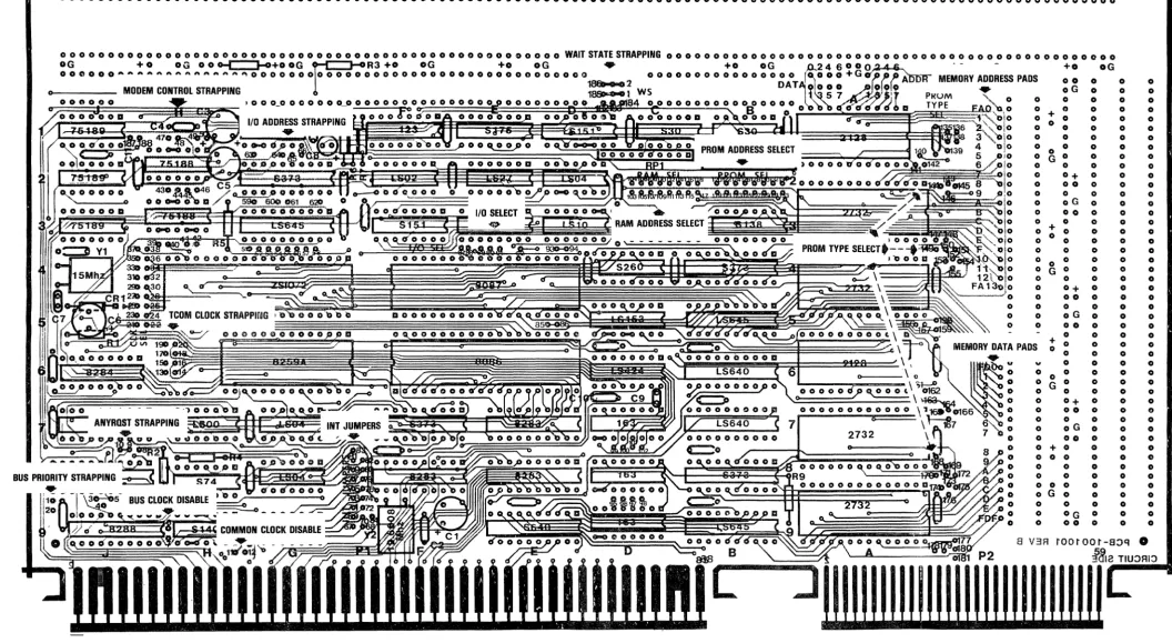
The FT -86C is shipped with the following options and straps. Option straps and IC's can be located by using the x-y coordinate system etched on the PCB. Along the length of the PCB is a set of alphabetic coordinates (A, B, 0, etc.). Along the width of the PCB, a set of numeric coordinates ( 1, 2, 3, etc.) can be found. These coordinates form an x-y grid so that straps and IC's can be located rapidly.
2.1 MUL TIBUS CONTROL
The FT -86C is optioned to act as bus master with the highest priority. This is done by a strap (pad 1 to pad 2 at board location 8J) which holds pin 9 of the 8289 to ground. (Refer to Figure 2-1 for pad locations and Figure 2-2 for specific strapping information.) Cutting the ground strap allows the FT -86C to respond to the Multibus bus priority in (BPRN) signal.
The FT -86C can be used in either parallel or serial bus priority arbitration schemes. F or parallel priority arbitration external logic must be provided.
The 8289 bus arbiter has the signal ANYRQST option strapped to ground via pads 9 and 10. (Refer to Figure 2-1 for pad locations and Figure 2-2 for specific strapping information.) In this mode the FT86C will not release the Multibus unless it has completed its immediate bus access requirements. Cutting the ground trace between pads 9 and 10, and strapping ANYRQST to the adjacent option hole (pad 8) will hold ANYRQST high. The FT -86C will now relinquish the bus as soon as the current bus transfer cycle (if any) has been completed.
ANYRQST BPRN CRQLCK FUNCTION
FACTORY Low Low Low Gives the FT -86e priority.
STANDARD It will not relinquish the
bus.
Low Dri ven by pin 15 Low The FT -86C will relinquish on Multibus the bus only to a higher
USER priority master.
OPTIONS Low Dri ven by pin 15 High The FT-86C relinquishes on Multibus the Multibus after each
transfer cycle.
2.1.1 MUL TIBUS OPTIONS (Figure 2-2)
The FT -86C is factory optioned to provide bus clock and common clock to the Multibus. The clocks can be disabled by cutting the straps between pads 6 and
7 and 11 and 12 (Refer to Figure 2-2 for pad locations). The FT -86C will now draw its bus clock from the Multibus.
2.2 COMMUNICATIONS OPTIONS
Most of the communications options for the FT -86C are software controlled. The strapping options for the communications channels allow the user to select the communications clock source and speed for each channel. The user can also select local mode (direct connection to a terminal) or select modem operation through a combination of software and hardware strapping options.
2.2.1 COMMUNICA TIONS CLOCK STRAPPING
500 0 0 0 \ \ 0 0 0 0
;!
0 0 0 0 0 0 0 0 0 0 0 0 0 2 4 9 0 0 0 0 0 0 0 0 0 0 0 0 0 0 0 0 0 0 0 0 0 0 0 0 0 10 0 0 0 0 0 0 0 0 0 0 0 0 0 0 0 0 0 0 0 0 0 0 0 0 0 0 0 0 0 0 0 0 0 0 0 0 0 0 0 0 0 0 0 0 0 0 0 0 0
0 0 0 0 0 0 0 0 0 0 0 0 0 0 0 0 0 0 0 0 0 0 0 0 0 0 0 0 0 0 0 0 0 0 0 0 0 0 0 0 0 0 0 0 0 0 0 0 0 0
0 0 0 0 0 0 0 0 0 0 0 0 0 0 0 0 0 0 0 0 0 0 0 0 0 0 0 0 0 0 0 0 0 0 0 0 0 0 0 0 0 0 0 0 0 0 0 0 0 0 0 0 0 0 0 0 0 0 0 0 0 0 0 0 0 0 0 0 0 0 0 0 0 0 0 0 0 0 0 0 0 0 0 0 0 0 0 0 0 0 0 0 0 0 0 0 0 0 0 0 0 0 0 0 0 0 0 0 0 0 0 0
o 0 0 0 0 0 0 0 0 0 0 0 0 0 0 0 0 0 0 0 0 0 0 0 0 0 0 0 0 0 0 0 0 0 0 0 0 0 0 0 0 0 0 0 0 0 0 0 0 0 0 0 0 WAIT STATE STRAPPING 0 0 0 0 0 0 0 0 0 0 0 0 0 0 0 0 0 0 0 0 0 0 0 0 0 0 0 0 0 0 0 0 0 0 0 0 0 0 0 0 0 0 0 0 0 0 0 0
oG + 0 oG OOo-t:=)-o+OOG F R 3 + 0 oG +0 o G . . +0 oG ..a...24600Q~ 0 - - +0 oG
o 0 CII 0 0 0 ... ,. . . .., 0 0 0 0 0 0 0 0 0 0 0 0 0 0 0 0 0 0 0 0 0 0 0 0 0 0 0 0 0 0 0 0 0 0 0 0 0 0 0 0 0 0 0 0 0 0 0 0 0 0 0 0 r~O 0 + G
CJ" ,. ,.
Al>15R"" MEMORY ADDRESS PADS 0 0 0'186D+o2 DAT~~ 0 0 9 G
o MODEM CONTROL STRAPPING 1~ WS 5 7
I
PKUM 0 00 0 0 0 0 , 0 0 0_0 0 0 0 0 0 0 _ 0 0 0 0 0 o~ 0 0
0
0 0 0 0 0 0 0 0 0 0 0 0 0 0 0 0 0Off
0 0 0 0 0 a TYPE 0 : : :I/O ADDRESS STRAPPING 0 0
f
0 0 0 0 a 0!
0 0..
: : :
o 0
o ~ 0 o o o o o o o o o o o o o 0 o 0 + o 00
o 0
o oG
o 0 0
o 0 0 + 0 0 0 0 o 0
0 0 G 0 0 0 0 0 0 + 0 v 0 0 0 G 0 0 0 0 0 0 0 + 0 0 0 0
o o 0
o 0
o 0 0 + 0 0 0 0 o 0 o G 0
00 0
o 0
o 0 o 0
0 0 0 0 + 0 0 0 oG 0 0 0 0 0 0 o 0
o o o o o o o o o o o o o o o 0 0 0 o G 0 o 0
o OG o
o 0 0 o
0 0 0 0 0 0 0 0 0 0 0 0 0 0 0 0 0 0 0 0 0 0 0 0 0 0 0 0 0 0 0 0 0 0 0 0 0 0 0 0 0 0 0 0 0 0 0 0 0 0 0 0 0 0 0 0 0 0 0 0 0 0 0 0 0 0 0 0 0 0 0 0 0 0 0 0 0 0 0 0 0 0 0 0 0 0 0 0 0 0 0 0 0 0 0 0
~
a ~
8 V3A tOOtOOt-80Q 0,,--.a..._--~::.ra11ft1
lOla
TIUOAIO::JIIIIII"""IIIIIIIIIIIIIIII"
Figure 2·1.
FT -86C SELECTED PAD LOCATIONS [image:13.1229.90.1147.81.660.2]BUS PRIORITY STRAPPING (CUT TO ENABLE BPRN)
ANYRDST STRAPPING
(CUT & JUMPER TO PAD 8 FOR ANYRDST HIGH)
Figura 2-2. MULTIBUS CONTROL STRAPPING
BUS CLOCK STRAPPING (CUT TO DISABLE)
COMMON CLOCK STRAPPING (CUT TO DISABLE)
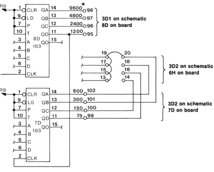
EXAMPLE 1 - Change Channel "B" to 9600
1. Cut trace between Ir 7D pin 11 and pad 99, to free trace from pad 99 to pad 16.
2. Add jumper between pads 98 and 99 to place 9600 baud clock on pad 16. 3. Cut jumpers between pads 15, and 17 to separate Channel tlA and Btl clocks. 4. Jumper pad 16 to pad 15, make sure jumper between 13 and 15 is intact.
*
R9 1 14
9600 98}
ClR OAlO OS 13 4800 097 301 on schematic
p OC 12 2400 96 80 on board
T 00 11 1200 95
A 80 00 15
4 163
S 20
5 C
6 0 18
} 302 on schamatlc
2 ClK 16 6H on board
14
R9 1 14 600 102
ClR OA
9 lD
OS 13 300 101 } 3D2 on schamatlc
7 p
QC 12 150 100 70 on board
10 T
QO 11 75 99
3 A 70 15 4 S 163 QO
5 C
I- 6 0
2 ClK
Figure 2-3. CLOCK GENERATOR STRAPPING
*
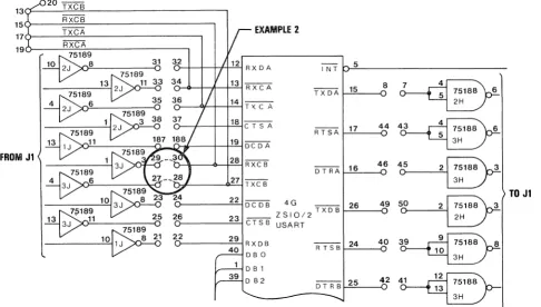
NOTE: Labeled baud are for 64 USART clock mode. [image:15.613.94.523.221.566.2]The FT -86C can also be strapped to operate from an external clock source. Figure 2-4 is a schematic representation of the telecommunications circuitry.
EXAMPLE 2 - OPERATE CHANNEL "B" FROM MODEM CLOCK
1. Remove jumpers between pads 13, 15, and 17 removing the internal clock from Channel "B".
2. Jumper pad 27 to 28.
3. Jumper pad 29 to 30. Clock now comes from Jl pins 44 for TXCB and 46 for RXCB.
20 TXCS
13~----~~---;
RXCS
150---~~---.
EXAMPLE 2
170---T~X~C~A~---__.
19o-____ ~RX~C~A~ ____________ __.
FROM J1
32
34
3n6t---OI--+--+=-14"'-1 T \( C A
0--+-t--lf-"18~ C T S A
~~
______
~~~r»__
~~~19~DCDA b-\---4~F28::..i R XC BtbI'---_--C~2.:...,7 T XC B
I N T b--'5~ ____________________ _
TXDA!---"15=--__ U8
~
- ~
RTSA 17 44
~
~'----G ~ ~
D T RA
~16=--
__ 4u6~
~ ~
22 DCDB 4G _ _ 26 49 5~2 75188 3
ZSIO/2TXDB~~--~ 2H
0-_ _ _ _ -=2.::...,3 C T S B USART
o-_ _ ---:2=.;:9'-! R X D B 40 DB 0
DB 1 39 D B2
40 3~9 75188 8
RTSB~24~ __ O 10
3H
42 4~12 75188
t-='---<U 13
3H
Figure 2-4.
MODEM CONTROL AND COMMUNICATIONS STRAPPING
TO J1
Additional straps may be needed if modem control signals are to be used. The complete list of the telecommunications option pads can be found in Table 2-1. By refering to this list the user should have no difficulty in strapping the telecommunications interface for his application.
[image:16.613.66.552.282.558.2]2-8
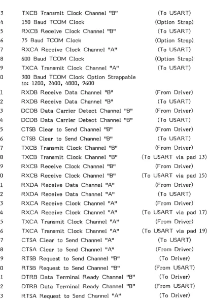
TABLE 2-1. TELECOMMUNICATION PAD ASSIGNMENTS
PAD
II
13 14 15 16 17 18 19
SIGNAL NAME
TXCB Transmit Clock Channel "B" 150 Baud TCOM Clock
RXCB Receive Clock Channel "B" 75 Baud TCOM Clock
RXCA Receive Clock Channel "A" 600 Baud TCOM Clock
TXCA Transmit Clock Channel "A" 20 300 Baud TCOM Clock Option Strappable
to: 1200, 2400, 4800, 9600 21 22 23 24
25
26 27 28 29 30 31 32 33 3435
36 37 38 39 40 41 42 43RXDB Receive Data Channel "B" RXDB Receive Data Channel "B"
DCDB Data Carrier Detect Channel "B" DCDB Data Carrier Detect Channel "B" CTSB Clear to Send Channel "B"
CTSB Clear to Send Channel "B" TXCB Transmit Clock Channel "B" TXCB Transmit Clock Channel "B" RXCB Receive Clock Channel "B" RXCB Receive Clock Channel "B" RXDA Receive Data Channel "A" RXDA Receive Data Channel "A" RXCA Receive Clock Channel "A" RXCA Receive Clock Channel "A" TXCA Transmit Clock Channel "A" TXCA Transmit Clock Channel "A" CTSA Clear to Send Channel "A" CTSA Clear to Send Channel "A" R TSB Request to Send Channel "B" RTSB Request to Send Channel "B" DTRB Data Terminal Ready Channel "B" DTRB Data Terminal Ready Channel "B" RTSA Request to Send Channel "A"
SOURCE/DESTIN A TION
(To USART) (Option Strap)
(To USART) (Option Strap)
(To USART) (Option Strap)
(To USART)
(From Driver) (To USART) (From Driver)
(To USART) (From Driver)
(To USART) (From Driver) (T a USAR T via pad 13)
(From Driver) (To USART via pad 15)
(From Driver) (To USART) (From Driver) (T a USAR T via pad 17)
(From Driver) (To USART via pad 19)
(To USART) (From Driver)
(To Driver) (From USART)
(To Driver) (From USART)
[image:17.613.113.525.123.718.2]TABLE 2-l. TELECOMMUNICA TION PAD ASSIGNMENTS (Cant.)
PAD II SIGNAL NAME SOURCE/DESTINA TION
44 RTSA Request to Send Channel "A" (From USART) 45 DTRA Data Terminal Ready Channel "A" (To Driver) 46 DTRA Data Terminal Ready Channel "A" (From USART) 47 TXDA Transmit Data Channel "A" (To Driver) 48 TXDA Transmit Data Channel "A" (F rom USAR T) 49 TXDS Transmit Data Channel
"B"
(From USART) 50 TXDS Transmit Data Channel"B"
(To Driver) 187 DCDA Data Carrier Detect Channel "A" (From Driver) 188 DCDA Data Carrier Detect Channel "A" (To USART)2.3 EPROM TYPE
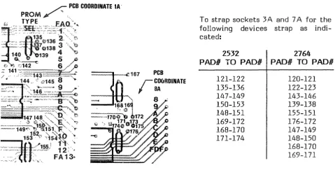
When ordered with firmware, chip locations 3A and 7 A will be strapped for the appropriate EPROM type. Locations 4A and 9A are capable of being user optioned for 2532, 2732, or 2764 parts. A gate must be added to use 2764 parts in locations 4A and 9A. If 2732 or 2532 parts are used they should be left justified in the EPROM pads, O.e. pin 1 of the 2732 or 2532 should be put in pin 3 of the EPROM pad and pin 24 into pin 26 of the pad).
To strap sockets 3.A and 7 A for the following devices strap as indi-cated:
2532 2764
PAOlI TO PAOli PAOli TO PAOli 121-122
135-136 147-149 150-153 148-151 169-172 168-170 171-174
Figure 2-5. EPROM STRAPPING
120-121 122-123 143-146 139-138 155-151 176-172 147-149 148-150 168-170 169-171
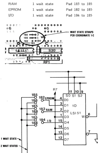
[image:18.615.61.541.481.734.2]2.4 WAIT STATE TIMING
Wait state timing is selected by straps at board location ID. Either one or two wait states may be inserted for RAM, EPROM or I/O. The selection of the number of wait states is dependent on the speed of the slowest device in each category. Refer to Figure 2-6 for strap locations.
To calculate the number of wait states required for a chip, take the response time of the chip and subtract 400 ns. Divide the result by 200 ns (the period of each wait state) and use the next highest multiple.
The factory settings are:
RAM 1 wait state Pad 183 to 185
EPROM 1 wait state Pad 182 to 185
I/O 1 wait state Pad 184 to 185
coo C '; - 0 0 0 0 0 0 0 0 0
QG
+0oG
WAIT STATE STRAPS PCB COORDINATE 1-C
R7
11 10 9
185 SO S1 S2
182EPROM 4
DO
186
185 3 01 10
186 183 RAM 2
02 LSI51
1 6
185 03 W
184 I/O 15
04
18
14
05
13
06
1 WAIT STATE 12 07
2 WAIT STATES
Figure 2-6. WAIT STATE STRAPPING
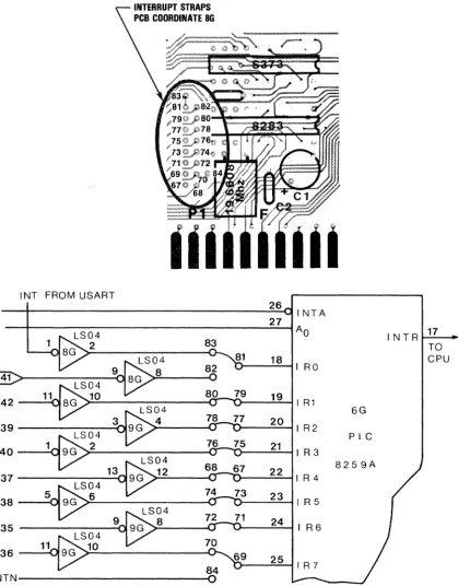
[image:19.613.145.460.223.711.2]2.5 INTERRUPT STRAPPING
Interrupts from the Multibus are available on the following pads:
INTERRUPT PAD ASSIGNMENTS
PAD II SIGNAL NAME SOURCEjDESTINA TION
67 IR4 (To PIC)
68 IR4 (From Multibus Driver)
69 IR7 (To PIC)
70 I1~7 (From Multibus Driver)
71 IR6 (To PIC)
72 IR6 (From Multibus Driver)
73 IRS (To PIC)
74 IRS (From Multibus Driver)
75 IR3 (To PIC)
76 IR3 (From Multibus Driver)
77 IR2 (To PIC)
78 IR2 (From Multibus Driver)
79 IRI (To PIC)
80 IRI (From Multibus Driver)
81 IR~ (To PIC)
82 IR~ (From Multibus Driver)
83 INT (From USART)
84 INTN (From Optional 8087)
Refer to Figure 2-7 for interrupt pad locations.
I NT FROM USART
@>
42 11
39
40
37 5 38
35
36 11
INTN
2-12
INTERRUPT STRAPS
PCB COORDINATE 8G
83
82
0
80
78
76
68
74
72
70
84
0
81
79
77
75
73
71
69 26
INTA
27
AO
18
I RO
19 I R1 20
I R2
21 IR3
22
23
24
figure 2-7.
INTERRUPT STRAPPINGINTR 17 TO CPU
6G
PIC
[image:21.617.101.521.108.645.2]SECTION 3.0
THEORY OF OPERATION FT -86C
The FT -86C processor is the Intel 8086 5 MHz 16-bit microprocessor. The 8086 communicates to the outside world via a 20-bit wide mUltiplexed address and data bus, i.e., addresses and data exist on the same pins but at different times. The separation of data and address values is achieved by using signals derived from the 8086 status lines. Eleven additional 8086 lines provide the timing and control interfaces. Internally, the 8086 can be considered as three major elements: the Bus Interface Unit (BIU), the Execution Unit (EU) and the timing and control unit.
The bus interface unit operates asynchronously to the execution unit. The BIU controls an internal 6 byte long instruction queue. The BIU will prefetch instructions from memory whenever there are 4 bytes or less in its internal queue and the executive unit doesn't require use of the bus. The BIU has access to 5 of the 8086's 16-bit registers.
The execution unit is not directly involved with bus management. The execution unit executes instructions taken off the internal 6 byte instruction queue that were prefetched by the BIU. When the EU requires immediate access to the bus, it does so via the BIU.
The control and timing unit provides status information to external devices in addition to the EU and the BIU. The processor status lines 50, 51 and 52, together with the processor clock, are provided to the external bus control elements to enable demultiplexing of the address and data lines from the 8086. The bus control elements also decode the status lines into the appropriate operational commands.
The 8087 numerical data processor operates in a close coupled configuration with the 8086. The 8087 can execute instructions in parallel with the 8086. The 8087 provides trigonometric, logarithmic, and exponential functions in addition to its arithmetic processing capabilities. The 8087 conforms to the proposed IEEE Floating Point Standard.
Internally, the 8087 consists of two units: a control unit and a numeric execution unit. The 8087 control unit maintains synchronization with the 8086 by monitoring the 8086 status lines SO, 51, 52, and 56. The 8087 control unit moitors the data bus to obtain 8087 specific instructions.
The numeric execution unit has a register stack of 8 80-bit data registers which are used for computation. Instructions can addres the data registers either implicitly or explicitly.
3.1 BUS ELEMENTS
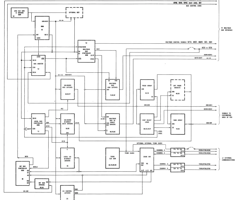
There are four major elements within the FT -86C bus system: bus control, local bus,
I/o
bus and the Multibus. Figure 3-1 is a block diagram of the FT -86C.3.1.1 BUS CONTROL
Bus CO(!t!IJ: is hlplemented Nith three LSI chips. The on-board bus and the I/O bus are controlled by an Intel 8288 bus controller. The Multibus is controlled by a second 8288. Selection of which bus controller to use is made through an Intel 8289 bus arbiter. The 8289 resolves access contention to the Multibus when operating in a multi-master environment.
3.1.2 LOCAL BUS
The 20-bit memory addresses output by the 8086/8087 are always latched on-board. A range test is then carried out by the memory decoding logic to determine if this is within the local (on-board) address range. If the address is not within this range the bus arbiter contends for access to the Multibus. The local bus controller is disabled and when access to the Multibus is granted the bus arbiter enables the Multibus bus controller. If the address is a valid local address the local bus controller is enabled and issues the appropriate commands and enable signals.
3.1.3
I/o
BUSThe local
I/o
bus consists of the low order 8-bits of both the data and address lines. It is activated for an input or output operation. TheI/o
bus is only acti ve for localI/o
addresses in the range 00 to 3F Hex.3.2 MEMORY
The on-board memory resides in two overlapped 64 Kbyte address areas. FOOOO to FFFFF Hex
00000 to OFFFF Hex
An address of Hex FFFFO will also address Hex OFFFO. This overlaid 64 Kbyte area is decoded into two sections of 32 Kbytes for EPROM and, 32 Kbytes for RAM.
3-2
3.2.1 RANDOM ACCESS MEMORY
The FT -86C comes with 4 Kbytes of RAM. This is at addresses Hex 00000 to OOFFF, and also Hex FOOOO to FOFFF. The RAM is configured with 2 x 8 Kbytes 200ns static RAMs.
Decoding is provided for up to seven additional pairs of RAMs up to a maximum of 32 Kbytes.
3.2.2 PROGRAMMABLE READ ONLY MEMORY
CPU ClK GEN
r-·---,
•
IIt DRIVERS OPTIONAL GCII7
l12li4
LT
_.J
6J
4 AOO-A013
-1!0811 IE
INT SO-S3
r-LOCK
9J SYSOIRESB
MULTIBUS SII BUS S3 C~NTROUER
8288 OT/R lOCK
AEN
SII·S3 AEN SYSS
BUS ARBITER
>---- CEIl
BJ
r'"" BCLK
il
-
AOO-A013ON·OOARO ADO LATCHES
r - r
-4D.BB.7F
.
ALE
J
SO-S3
r---ON·BOARO
LOCAL BUS OE.I BI·DIRECT
~
COIHROLlER DATA DRIVERS
8288
~
~
CEN 50.9BlJ
-OIR
DT/R
E
INTR
I - LDCAL 110 ~
J
BI·DlRECT DRIVERS3G INT BUS INTA·2
CDNTRDUER 8259 DO
07 AB 68
IRO
ro-
INT BUS IRO IRlDRIVERS
~
8G.9G
OABl
lal·IRl 110 CD~TRDl
L-....o- LATCHES GAB2
ZG
ALEl
r
I
-1
DE STB MULTIBUS
BUS ADO LATCHES
AIH
I--lE.BE.BF
~ OIR OTIRl MULTIBUS
BUS BI· ADD DIRECT ADF DRIVERS
- 6 6B.1B.9E
TCOM CLOCK TCOM
CLK GEN
60.1D.8D.90
PROM ARRAY r<>- AIN
-3A.7A
CS
-ABB·ABO
r-CHIP SELECT
-LOGIC
-3B.3C.3E.3F
LRSEL
l
LPSELIIlTERRUPT REQUESTS IRllRl
iPIiJj. iiiiEli. IiPiilf. BUSY CBRn. INIT BUS CONTROL lOGIC
MULTIBUS CONTROL SIGNALS INTA1. MR01. MWR1. IOR1. 10Wl
..,,--
.... BCLK & CCLK1
AORO-AOR13
OATO·OATF
--r--"
I OPT PROM I
I
SOCKETS Ir-I
AIN I----I 4A.BAI
CS
L __
-I
ABO-AB13
IOCSO·IOCS7
I
RAM ARRAY"'- AIN OBO·DBF CS
lA.6A
•
.
Pl MULTIBUS DUS INTERFACE
SIGNALS TO CUSTOMIZING AREA OF PCB
OPTIONAL EXTERIIAL TCOM CLOCK
I
CHANNEL 0 ~
CHANNEL A ZILDG SID
D80 4G
r
CHANNEl ADB7
CHANNEl D BIA CIO INT
I
--TTL TO EIA r---u CH B TIL TO EIA
CHA
EIA TD TIL CHA EIA TO TIL
CHB
Figure 3-1.
'0 RXOB.CTSB.DCDB RXOA.CTSA.OCOA TXDA.RTSA.DTRA TXDB.RTSB.OTRB •
Jl EXTERNAL COMMUNICATIONS
[image:24.1224.349.1151.40.723.2]If the FORTH monitor is ordered with the FT -86C it will be in 32 Kbit EPROMs located at board positions 3A and 7 A. The FORTH monitor resides at memory addresses Hex FEOOO through Hex FFFFF, and also at addresses Hex OEOOO through, Hex OFFFF.
If the 8087 numeric data processor option is ordered, an enhanced FORTH system is supplied in EPROM. The enhancements follow the guidelines of the proposed standards committee working group version of Floating Point FORTH.
3.3 TIMING
Two timing elements are used in the FT -86C: the processor clock and the bus clock. The processor clock is generated by an Intel 8284. The oscillator input is 15 MHz. The 8284 divides by three and provides a 5 MHz 33% duty cycle clock to the processor and to the bus control elements.
The bus clock can either be generated by the FT -86C and fed onto the Multibus or can be driven via the Multibus from another bus master. The bus clock is used by the bus arbiter in its bus contention circuits and also to synchronize its output commands to the bus controllers.
3.3.1 CLOCK GENERATOR
In addition to providing the processor clock, the 8284 synchronizes and controls the READY and RESET lines to the 8086/8087. Generation of the Multibus initialization signal INIT holds the RESET line active.
The READY line to the 8086 is controlled by two pairs of input signals on the 8284. One pair of inputs are used for controlling wait states for on-board devices, the other pair is used for external bus control, i.e., Multibus.
3.3.2 PROCESSOR TIMING
The 8086 processor cycle operates in a minimum of four clock cycles called Tl, T2, T3, and T4. Depending on the speed of attached memory or I/O devices a variable number of wait states may be inserted between processor clock cycles T3 and T4 (e.g., Tl, T2, T3, Tw ••• Tw, T4.)
The FT -86C provides separately strappable wait states for on-board I/O, RAM and EPROMs. Multibus access, being asynchronous, will automatically result in
o
to N wait states being inserted. The number of wait states inserted depends on bus contention and arbitration and also on the access time of the specific device or memory type accessed.3.3.3 BUS CONTROL TIMING
The three elements that make up the bus control section derive their timing from the processor clock and the processor status lines (SO, 51, and 52) to
indicate what function is going to be performed during the current Tl to T4 cycle. This is done at Tl. The 8086 also places the address on the multiplexed bus at this time.
Both bus controllers (8288s) use the status lines and the processor clock to generate a pulse (ALE) to latch the address into both the local bus and the Multibus address drivers. The Multibus address drivers do not at this stage have their outputs enabled.
The output of the local address drivers is decoded by the local PROM, RAM and I/O decoders to establish whether this address falls within the on-board address range. If it does, a signal is generated and input to the bus arbiter to indicate a resident bus access only. The Multibus address latches are not output enabled and the Multibus bus controller is held disabled. If the address is not within the resident address space, the signal to the 8289 bus arbiter is raised and the 8289 contends for the Multibus. As soon as the 8289 has gained control of the Multibus, the Multibus address drivers are enabled as is the Multibus bus controller.
At T2 time the 8086 floats its multiplexed address/data lines preparatory to outputting or inputting data. If the resident bus controller is enabled, it will now generate the appropriate command which has been decoded from the processor status lines. If the Multibus bus controller is enabled, the appropriate commands are issued to the Multibus and the resident bus controller is held disabled.
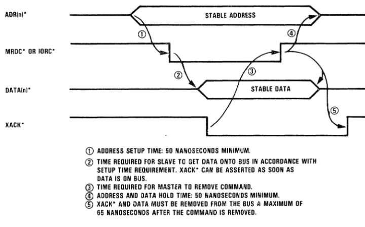
At T3 the appropriate control signals are issued from whichever bus controller is active to condition one of the sets of data bus transceivers. The control signals will be held active through T3 and Twait, where Twait may be 0 up to N. The number of Twaits is dependent on the speed of the addressed device. When addresses are within resident bus address space, the FT -86C allows the user to strap select separate wait states for EPROM, RAM and I/O. When addresses are not within the resident bus space, Twait will be issued until the addressed Multibus device responds with an acknowledgement (XACK).
At T4 time the 8086 floats its address/data lines preparatory to issuing a new address at the following Tl. The commands are terminated as are the control signals. The processor status lines (50, 51, and 52) all go inactive.
3.3.4 BUS TIMING
Although the Multibus is an asynchronous bus, two clock lines are present on the bus -- bus clock and constant clock. The Multibus also has certain timing constraints regarding the relationship of the address, data and command presentation. Bus clock is used to synchronize bus arbitration. Enabling of the Multibus address drivers (AEN) is synchronized with bus clock; however, the disabling of the Multibus address drivers is synchronized with T4 of the processor clock. Bus clock can, in theory, be any frequency; however, the lower the frequency the longer the Multibus access arbitration time. The FT -86C generates a bus clock frequency of 9.83 MHz.
ADR(nj'
MRDC' OR 10RC'
DATA(nj'
XACK'
STABLE ADDRESS
STABLE DATA
~
_ _
---,I
CD ADDRESS SETUP TIME: 50 NANOSECONDS MINIMUM.
@ TIME REQUIRED FOR SLAVE TO GET DATA ONTO BUS IN ACCORDANCE WITH SETUP TIME REQUIREMENT. XACK' CAN BE ASSERTED AS SOON AS DATA IS ON BUS.
® TIME REQUIRED FOR MASTER TO REMOVE COMMAND.
@) ADDRESS AND DATA HOLD TIME: 50 NANOSECONDS MINIMUM. ® XACK' AND DATA MUST BE REMOVED FROM THE BUS A MAXIMUM OF
65 NANOSECONDS AFTER THE COMMAND IS REMOVED.
Figure 3-2. ADDRESS TIMING COMSTRAINTS
3.4 COMMUNICA nONS
Two independent communications ports are provided via a Zilog ZSIO USART. Each port can be configured via software to operate in several different modes. Two full sets of RS-232C modem control signal drivers are provided, allowing modems to be attached to these ports. Access to these I/O ports is achieved through the FORTH words P@ and PI. These words are described in Section 5.0. All port programming and I/O is accomplished using these two words.
BASE ADDRESS (Hex)
0000 0002
0004 0006
ZSIO PORT Channel "A" Data
Channel "A" Control Registers Channel "B" Data
Channel "B" Control Registers
[image:27.615.119.479.105.329.2],...
CHANNEL AINTERNAL CHANNEL A CONTROL READ/WRITE
5Y GND LOGIC REGISTERS
~ ~ ~
DISCRETE....
CONTROL &~
STATUS (CH. AI
8
DATA
CPU INTERNAL BUS
6
CONTROL BUS I/O
DISCRETE CONTROL &
STATUS (CH. BI INTERRUPT CHANNEL B
CONTROL READ/WRITE LOGIC REGISTERS
H!
....
~ CHANNEL BINTERRUPT CONTROL
[image:28.617.73.538.107.347.2]LINES
Figure 3-3. USART INTERNAL STRUCTURE
~}
f--}
~
f---§}
==}
==:J
-.=}
:=}
--SERIAL DATA
CHANNEL CLOCKS
MODEM OR OTHER CONTROLS
MODEM OR OTHER CONTROLS
SERIAL DATA
CHANNEL CLOCKS
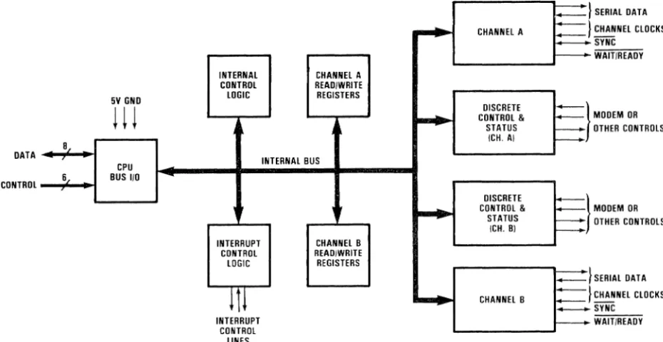
The USAR TIs internal structure includes a CPU interface, internal control and interrupt logic, and two full duplex channels. Each channel contains read and writ.e registers, and discrete control and status logic that provides the interface to modems or other external devices (see Figure 3-3).
The read and write register group includes five 8-bit control registers, two sync character registers and two status registers. The ZSIO interrupt vector capability is not used. All interrupt vectors are provided by the 8259A PIC. The registers for both channels are designated in the text as follows:
WRO-WR7
RRO-RR2
write registers 0 through 7 read registers 0 through 2
3.4.1 READ REGISTER FUNCTIONS
RRO Transmit/receive buffer status, interrupt status and external status
RRI Special receive condition status
RR2 Modified interrupt vector (Channel "B" only)
3.4.2 WRITE REGISTER FUNCTIONS
WRO Register pointers, CRC initialize, initialization commands for the various modes, etc.
WRI Transmit/receive interrupt and data transfer mode definition WR2 Interrupt vector (Channel "B" only)
WR3 Receive parameters and control
WR4 Transmit/receive miscellaneous (parameters and modes)
WR5 Transmit parameters and controls WR6 Sync character or SOLC address field WR7 Sync character or SOLC flag
The logic for both channels provides formats, synchronization and validation for data transferred to and from the channel interface. The modem control inputs Clear to Send (CTS) and Data Carrier Detect (OCO) are monitored by the discrete control logic under program control. Strapping options permit on-board emulation of the modem control signals. The automatic interrupt vectoring capability of the ZSIO is not used. An attempt to use the ZSIO generated interrupt vectors will cause an indeterminate result.
Both channels contain command registers that must be programmed prior to operation. The controlFORTH monitor initializes Channel "A and B" of the ZSIO.
3.4.3 PROGRAMMING THE WRITE REGISTERS
The Z8D-SID contains eight registers (WRO-WR7) in each channel that are programmed separately by the system program to configure the functional personality of the channels. With the exception of WRD, programming the write register requires two bytes. The first byte contains three bits (00-02) that point to the selected register; the second byte is the actual control word that is written into the register to configure the Z8D-SID. (See Figure 3-5.)
WRD is a special case in that all the basic commands (CMOD-CM02) can be accessed with a single byte. Reset (internal or external) initializes the pointer bits 00-02 to point to WRO.
3.4.4
PROGRAMMING THE READ REGISTERSThe ZBO-SIO contains three registers, RRO-RR2 (Figure 3-1) that can be read
to obtain the status information for each channel (except for RR2 -- Channel "B" only). The status information includes error conditions, interrupt vector and standard communications-interface signals.
To read the contents of a selected read register other than RRO, the user program must first write the pointer byte to WRO in exactly the same way as a write register operation. Then by executing an input instruction, the contents of the addressed read register can be rEad.
The status bits of RRO and RRI are grouped to simplify status monitoring. This enables tIle user to read all the appropriate error bits from aile register (RR!).
READ REGISTER 0
I
07I
06I
05 J 04J
03 J 02 J 01I
00I
I
I
I
READ REGISTER 1 t
I 071 06 I 051 04 1 03 I 02 I 01 1 DO 1
1 FIELD BIT HI PREVIOU BYTE 1 0 0 0 0 1 0 0
1 1 0 0 0 0 1 0
1 0 1 0 0 1 1 0
1 1 1 1
0 0 0 2
- PARITY ERROR Rx OVERRUN ERROR CRC/FRAMING ERROR ENO OF FRAME (SOLCI
tuSEO WITH SPECIAL RECEIVE CONDITION MODE
READ REGISTER 2
I 07 I 06 1 05/ 04
J
03 1 02 1 01 1 00 1I
I
tvARIABLE IF "STATUS AFFECTS VECTOR" IS PROGRAMMED
I
Rx CHARACTER AVAILABLE INT PENDING (CH. A ONL YI Tx BUFFER EMPTY } OCO
SYNC/HUNT
CTS •
Tx UNDERRUN/EOM BREAK/ABORT
·USEO WITH "EXTERNAL/ST.UUS INTERRUPT" MODE
ALL SENT S 1 FIELD BITS IN S SECONO PREVIOUS
BYTE 3 4 5 6 7 8 8 8
-RESIDUE DATA FOR EIGHT Rx BITS/CHARACTER PROGRAMMED
'10 }
Vlt
V2t
V3t INTERRUPT V4 VECTOR V5
[image:30.615.174.438.270.638.2]V6 V7
WRITE REGISTER 0
I
07I
06I
05 1 04I
03I
02I
0 II
00I
I I Io 0 0
o 0 I o I 0
o I I
I 0 0
I 0 I
I I 0
I 1 1
o 0 NULL COOE
REGISTER 0 REGISTER 1 REGISTER 2 REGISTER 3 REGISTER 4 REGISTER 5 REGISTER 6 REGISTER 7
o 1 SEND ABORT ISOLC)
1 0
1 1
RESET EXT/STATUS INTERRUPTS CHANNEL RESET
o 0 o 1
ENABLE INT ON NEXT Rx CHARACTER RESET TxINT PENDING
1 0 ERROR RESET
1 1 RETURN FROM INT ICH·A ONLY)
o rWLL CODE
o RESET Rx CRC CHECKER 1 RESET Tx CRC GENERATOR 1 RESET Tx UNDERRUN/EOM LATCH
WRITE REGISTER 1
I
07I
06I
051 04I
03I
02I
01I
DOI
I
I
EXT INT ENABLEL -_ _ _ _ _ Tx INT ENABLE
L -_ _ _ _ _ _ _ STATUS AFFECTS VECTOR ICH. B ONLY)
Rx INT DISABLE
Rx INT ON FIRST CHARACTER } INT orl ALL Rx CHARACTERS IPARITY AFFECTS VECTORI • INT ON ALL Rx CHARACTERS IPARITY DOES NOT AFFECT VECTOR)
- WAIT/RE/jOY 011 R/T ' - - - - WAIT/READY FUNCTION ' - - - WAIT/READY ENABLE
WRITE REGISTER 2 (CHANNEL B ONLY)
I
07I
06I
051 04I
03I
02I
01I
00I
I I
I
IWRITE REGISTER 3
I
07I
06I
05 1 04I
03I
02I
01I
DOI
• OR ON SPECIAL CONDITION
VO } VI V2
V3 INTERRUPT V4 VECTOR V5
V6 V7
I I
L~'====
Rx ENABLE SYNC CHARACTER LOAO INHIBITL
_~~======= ADDRESS SEARCH MOOE ISDLC) Rx CRC ENABLE ENTER HUNT PHASE ' - - - AUTO ENABLESo Rx 5 BITS/CHARACTER 1 Rx 7 BITS/CHARACTER
o Rx 6 BITS/CHARACTER I Rx B BITS/CHARACTER
WRITE REGISTER 4
' - - - - PARITY ENABLE
L -_ _ _ _ PARITY EVEN/OOO SYNC MODES ENABLE
1 STOP BIT/CHARACTER III STOP BITS/CHARACTER
2 STOP BITS/CHARACTER
o 1
o
1
8 BIT CHARACTER 16 BIT SYNC CHARACTER SOLC MODE 101111110 FLAG) EXTERNAL SYNC MOOE
XI CLOCK MODE X16 CLOCK MODE X32 CLOCK MODE X64 CLOCK MODE
WRITE REGISTER 5
I
07I
06I
051 04I
031 02I
01T
DO-I
I
I
IL~I~=== ~~SCRC
ENABLESOLC/CRC·16
L -_ _ _ _ _ _ _ _ Tx ENABLE
L-_ _ _ _ _ _ _ _ _ SEND BREA~
"--DTR
Tx 5 BITS lOR LESS) CHARACTER Tx 7 BITS/CHARACTER Tx 6 BITS/CHARACTER Tx 8 BITS/CHARACTER
WRITE REGISTER 6
I
07T
06T
051041 03I
02I
01T
DO1
I
I
I
I-ALSO SDLC ADDRESS FIELD
WRITE REGISTER 7
I
07I
06I
051 04I
03I
02I
01I
00I
I I
I
I'FOR SOLC IT MUST BE PRO GRAMM EO TO "01111110" FOR FLAG RECOGNITION
SYNC BIT 0 } SYNC BIT 1 SYNC BIT 2 SYNC BIT 3 • SYNC BIT 4 SYNC BIT 5 SYNC BIT 6 SYNC BIT 7
SYNC BIT 8 } SYNC BIT 9 SYNC BIT 10 SYNC BIT 11 SYNC BIT 12 • SYNC BIT 13 SYNC BIT 14 SYNC BIT 15
Figura
3·5.
WRITE REGISTER BIT FUNCTIONS3.5 INTERRUPT CONTROL
The 8259A programmable interrupt controller is in local I/O space at Hex address 0008. It can be programmed using the P@ and P! commands in the same manner as the serial communications ports.
When an interrupt request is generated and presented to one of the 8259 A interrupt request lines, the interrupt controller will evaluate the interrupt request and, if appropriate, generate an interrupt request to the 8086. If interrupts are enabled, the processor will complete execution of the current instruction and enter the interrupt acknowledge machine cycle. The processor status line S2 being low indicates either an I/O operation or an interrupt machine cycle. The
I/o
bus will be enabled. The local 8288 bus controller generates an interrupt acknowledge signal (INTA) which is used to precondition the 8259A interrupt controller. No other activity takes place during this processor cycle. The second processor cycle duplicates the first up to issuing the INTA. The second INTA causes the 8259A to issue a vector byte to the 8086 via the I/O data bus transceiver. The vector byte is used to generate an address where the 8086 loads a new code segment and instruction pointer.The base address of the interrupt controller is Hex 0008. Address line 1 is used to indicate the first word of either an initialized command word or an operational command word. For full programming information see the Intel Component Data Catalog, or the 8086 User's Guide.
SECTION 4.0
BREADBOARD INTERFACE
4.1 MEMORY ADDRESS BUS
The memory address bus is available at two locations. The full 20-bit address is available at pads FAD through F A13. The lower 8-bits of the address lines are available on pads at board location AD also. Refer to Figure 4-1 for pad location.
Memory addresses are always presented at these locations even when the address is not within the on-board address range.
4.2 I/O ADDRESS BUS
The I/o address bus is the lower 8-bits of the address bus. The I/O address bus is always active when any address is output from the 8086.
The addresses are available at board area G2. See Figure 4-2 for pad layout and numbering.
4.3 DATA LINES
Two separate sets of data transceivers are available. One is active during memory references or memory mapped I/O operations. The other is only active during input, output or interrupt acknowledge processor cycles.
4.3.1 MEMORY DATA BUS
Memory data lines are available to the user at pads FDO through FDF. During an on-board memory write cycle, data will be valid on these pads during T3, Tw •• Tw. Tw is governed by strap settings at board location 01 (see Wait State Timing Section). During an on-board memory read, data should be presented during T3, Tw Tw, Tw. See Intel 8086 product specification for exact timings. During off-board operations, the on-board transceivers will be tri-stated, allowing pads FDO through FDF to float. The low order byte of the data bus is also available at board location AI. Refer to Figure 4-1 for pad location.
4.3.2 I/o DATA BUS
The I/O data bus is the low order byte of the data bus. It is only active during an input, output or interrupt acknowledge processor cycle. Timing is the same as the memory data bus. Wait states are set by straps at 02 (see Section on Wait State Timing).
4-2
7
2732
~
0 0 0
o
o
o
~
"
oG 0
o o o o o
¢ 0 0 0
0 + 0 0 0 0 0 0 0 0 0 0 0 0 0 0 0 0
o G o o 0 0 0
o
0G
0o 0 0 0
o
o o o
(;
"
o o
~
..
0
0
(,
0 0 0 0 0 0 0 0 0
0 0 0 0 0 0
4)
0
tOOtOOt-80Q
0
tala TIUOAlO
-::JIIIIIIIIIIIIIIIIIIIIIIIIIIIIII
4.4
I/o
SELECT LINESPADII
51 52 53 54 55 56 57 58 59
60
61 62 63 64 65
[image:35.613.122.257.140.314.2]66
Figura 4-2. 110 ADDRESS PADS
I/o
ADDRESS (Hex)0DB~
00B1 0DB2 00B3 00B4 0DB5 0DB6 00B7 0AB0 0AB2 0AB4 0AB6 0AB1 0AB3 0AB5 IDAB7
All
I/o
addresses in the range of Hex 00 to Hex 53 are automatically considered on-board addresses even though not all of theI/o
addresses are decoded.The I/O select lines are decoded on 8 byte boundaries. Address line
a
is not used. All I/O port addresses must be even addresses. Address lines 2 and 1 are available for port addressing within the selected chip. Select linesa
and 1 are used for the ZSIO and 8259A respectively. Refer to Figure 4-3 for I/O select line information.4.5 CHIP SELECT DECODING
Chip select lines are provided for RAM, EPROM and I/O. Spare lines are available for user added components.
4.5.1 EPROM CHIP SELECTS
ERPOM chip select lines are available on pads at board location B2. Select lines are decoded on 8 Kbyte boundaries. If the user adds PROM's using the spare select lines they must be connected to the opposite pad in order to be within the on-board address space. Only the top 4 chip select lines may be used, allowing the user to put a maximum of 32 Kbytes of EPROM on-board.
4-4
One chip select line is provided for 2764 EPROMs. This is derived from ORting the top two chip select lines on pads 119 and 121. If 2764s are to be used, pads 119 and 121 must be strapped to 120 and 122 respectively. Refer to Figure 4-4 for pad location.
BASE ADDRESS In Hex
OEOOO or FEOOO
OCOOO or FCOOO
OAOOO or F AOOO
08000 or F8000
I/o
ADDRESSES In Hex 0000-0007 0008-000F 0010-0017 00l8-00lF 0020-0027 0028-002F 0030-0037 0038-003FPAD
121 119 123 125
CHIP SELECT PAD NUMBER
91 90 89 88 87 92
TO PAD
122 120 124 126
SELECTED DEVICE
ZSIO 8259A SPARE SPARE SPARE SPARE SPARE SPARE
;~ .... t.: ... ;';"; ... -... ;;;;-;;,;,.;;;;-;;;;,;;;;-="' ... =-~..c.,,~-.,.I!IIIIIIIIIi--~
•.. , .. - . ....
[image:36.613.187.436.502.743.2]4.5.2 RAM SELECT LINES
The RAM select lines are decoded on 4 Kbyte boundaries. One select line is used to select the 2 Kbit by 8 RAM chips at board locations lA and 6A. Seven select lines are avilable for use options. To be included in the on-board RAM space the user must connect the appropriate pad to the pad opposite it in addition to wiring the select signal to the RAM chip. Refer to Figure 4-4 for pad location.
BASE ADDRESS OF CHIP SELECT CONNECT TO SELECT LINE (Hex) PAD NUMBER PAD NUMBER
00000 01000 02000 03000 04000 05000 06000 07000
or FOOOO 117
or FlOOD 115
or F2000 113
or F3000 III
or F4000 109
or F5000 107
or F6000 103
or F7000 105
0 0 0 0 0 0 0 0 0 0 0 0 0 0 0 0 0 0 0 0 0
~@
@G
+@@G
o@@cccccccoooccoOAT
ws
[image:37.618.122.494.186.684.2]118 116 114 112 110 108 104 106
figure
4-4.
EPROM AND RAM CHIP SELECT liNES
RAM SELECT
SECTION 5.0 FIRMWARE
5.1 CONTROLFORTH
ControlFORTH is supplied in EPROM and is an implementation of FORTH derived from fig-FORTH and with certain extensions. The extensions are a general set of monitor commands to assist the user in adding, debugging and testing LSI devices. This Section explains the monitor enhancements of controlFORTH in detail. The glossary in Appendix A contains descriptions of the other FORTH words in controlFORTH. For further information on FORTH, Appendix B is a bibliography of FORTH works.
In the following text underlines indicate one or more spaces and -+ means the RETURN key. With the exception of the substitute command all addresses, counts and value fields may be entered in decimal, octal or hexadecimal depending on the base selected prior to entering the command. Commands may be strung together, separated with spaces, on the same line with a carriage return ( -+ ) at the end. Once a base is selected it will remain in effect until another base command is entered. Base commands:
HEX -+ DECIMAL -+
OCTAL -+
Sets hexadecimal base Sets decimal base Sets octal base
The base selected will affect the number of characters displayed in any numeric field. All command formats shown use the hexadecimal base. See the glossary for more information.
5.2 MONITOR COMMANDS - Implied Segment Value
5.2.1 STUFF
FORMAT AAAA CCCC VV
AAAA CCCC VV STUFF Source address
Byte count
Value to be inserted
The STUFF command executes using the implied segment value. Memory will be filled with the specified value VV starting at address AAAA for the number of bytes specified in CCCC. See 5.4.1 for information on setting or viewing the implied segment value. The 16-bit implied segment value and 16-bit addresses are used together to generate the 20-bit addresses of the 8086. See the biblography in Appendix B for more information the 8086.
5-2
EXAMPLE: HEX COO 10 55 STUFF ~
This example fills 16 decimal (hexadecimal 10) memory locations starting at hexadecimal address COO with hexadecimal 55.
5.2.2 SUBSTITUTE FORMAT AAAA
DISPLAY FORMAT SS55 AAAA HH
AAAA SUBSTITUTE Starting address
This command executes on successive byte memory locations. If the contents of a byte location do not need to be changed, pressing carriage return will not alter the current value HH and fetch the next byte location. To change a value enter the required value VV and press carriage return. The entered value VV will replace the original value HH.
To terminate the SUBSTITUTE command press the Q key and carriage return. SUBSTITUTE operates in hexadecimal but it preserves and restores the base in use prior to using SUBSTITUTE.
5.2.3 MOVE
FORMAT AAAA BBBB CCCC MOVE
AAAA Source address
BBBB Destination address
CCCC Number of bytes to moved
This command moves the specified number of bytes from locations starting at AAAA to locations starting at BBBB within the implied segment. The move is always to higher memory locations.
5.2.4 MATCH FORMAT AAAA BBBB
ccce
AAAA BBBB CCCC MATCH Source address 1
Source address 2
Byte count to compare DISPLAY FORMAT FOR MISMATCH
IIII AAAA HH
nn
BBBB VVMATCH compares two given strings of bytes. The start addresses are AAAA and BBBB. This command will terminate either on completion of the count CCCC or after a given number of mismatches have been displayed. The number of errors tolerated before termination can be altered, see Section 5.4.3. This default is set to 10 mismatches.
5.2.5 P! and WP! FORMAT VV
DD
VV DD P! and VV DD WP! Value to be output to the port Destination port address
The commands P! and WP! write data to output ports. P! works with 8-bit ports and WP! is for 16-bit output ports. If the destination port address is within the local Con-board) I/O address space these commands will terminate normally even if there is no port at that address. If the destination port is in the off-board I/O address space, i.e., via the Multibus, two conditions can occur. If the destination port responds, the commands will terminate normally. If the destination port doesn't respond, the deadman timer will expire and terminate the command. In the second case there will be a delay of at least 1/10th of a second. Using a "TIMES • • . RUN" command it is simple to detect a non-responsi ve port.
5.2.6 P@ and WP@ FORMAT DD
DD _P(8) and DD _ WP@ Input port address
The commands P@ and WP@ read data from a given input port. Again, P@ is for 8-bit ports and WP@ is for 16-bit ports. These commands will exhibit exactly the same symptoms as the OUT command if the addressed port does not respond. The data value displayed will be indeterminate if the port does not respond. To see the value read from the port type the FORTH print command • "dot" or U. See glossary for more information about dot.
EXAMPLE: to view the value from an I/O device at Hex port II2E type:
5.2.7 GO
FORMAT AAAA GO
AAAA Address of first instruction to execute This command transfers control to the program whose first instruction is located at address AAAA and with the implied segment value.
5-4
5.2.8
5.2.9
RECEIVE FORMAT AAAA CCCC DD
SEND FORMAT AAAA CCCC
AAAA CCCC DD RECEIVE
Address where input data is to be loaded Count of bytes to be loaded
Input port address
AAAA CCCC DD SEND
Address where output data begins
Number of memory bytes to be transferred
DD Output port address
TRANSMISSION FORMAT HHHHHHHH etc.
Where each H is an ASCII character containing 4 of the B-bits in a byte. To SEND n bytes requires transmission of 2 n characters. The command pair RECEIVE and SEND receive and send binary data via a selected serial input/output port. The binary data is broken into 4-bit nibbles and converted to form the ASCII Hex characters D through 9F and AD through F for transmission over a serial link. The format for both commands is simply one of a long string of ASCII characters. The command SEND assembles the ASCII from the data bytes and transmits it. The RECEIVE command accepts an ASCII string, strips the ASCII, reassembles the original data bytes, and places them in memory at the given address.
5.2.10
DUMPFORMAT AAAA CCCC
DISPLAY FORMAT
AAAA CCCC DUMP Starting address Byte count
5.3 MONITOR COMMANDS WITH EXPLICIT SEGMENT ADDRESSES
5.3.1 SMOVE FORMAT AAAA SSSS BBBB
DDDD CCCC
AAAA SSSS BBBB DDDD CCCC SMOVE
-
-Source address within source segment Source segment address
Destination segment
address within
Destination segment address Count of bytes to be moveel
destination
The command SMOVE functions in the same way as MOVE except that the segment values must be explicitly specified.
5.3.2 SMATCH FORMAT AAAA SSSS BBBB DDDD CCCC
DISPLAY FORMAT SSSS AAAA HH
AAAA SSSS BBBB DODD CCCC SMA TCH
-
-First source address within source segment First source segment register address
Second source address within segment Second source segment register address Count of bytes to be compared
DODD BBBB VV
Command terminates either on completion of count or upon a gi ven number of mismatches, see Section 5.4.3.
5.4 MONITOR CONTROL COMMANDS
5.4.1 SEGMENT FORMAT SSSS
SSSS SEGMENT
Value to be loaded into the implied segment register. The contents of the implied segment may be views by typing: IMPLIED? -+.
(Note: If the number appears negative type: IMPLIED _@_U._ -+ ).
5.4.2 TIMES • . . RUN FORMAT
NNNN COMMAND
NNNN TIMES COMMAND RUN Loop counter value
One or more of the monitor commands using either implied or explicit segment register. The TIMES • . • RUN command pair must be used as a pair and in the order given above. The commands that go between TIMES and RUN will be executed at least once even if a zero is given for the count. The maximum count is 32,767. The number of commands that go in between has no practical limit and may extend over several lines. Each command must be able to be found in controlFORTH's dictionary or an error will result.
5.4.3 TOLERATED
To set the number of mismatches tolerated before termination of MATCH or SMA TCH type:
n TOLERATED -+
APPENDIX A
CONTROLFORTH GLOSSARY
This glossary contains the definition of all words in the controlFOR TH vocabulary. The de finitions are presented in ASCII sort order.
Stack Notation
The first line of each entry shows a symbolic description of the action of the procedure on the parameter stack. The symbols on the left indicate the order in which input parameters have been placed on the stack. Three dashes " ___ " indicate the execution point; any parameters left on the stack after execution are listed on the right. In this notation, the top of the stack is to the right.
Symbol Definition
addr,adrl,
b
c d,di,
flag ff n,nl, u,ul, ud,udi, tf
Pronunciation
Memory address
8-bit (with high eiaht bits zero)
7-bit ASCII character (with high nine bits zero) 32-bit signed double integer, most significant portion with sign on top of stack
Boolean flag (0
=
false, non-zero = true) Boolean false flag (value =0)
I6-bit signed integer number I6-bit unsigned integer number 32-bit unsigned number
Boolean true flag (value - non-zero)
The natural language pronunciation of controlFORTH names is given in double quotes
(").
Integer Format
Unless otherwise noted, all references to numbers are for I6-bit signed integers. For 32-bit signed double numbers, the most significant part (with the sign) is on top. All arithmetic is implicitly I6-bit signed integer math, with error and underflow indication unspecified.
Capitalization
Word names as used within the glossary are conventionally written in upper case characters. Lower case is used when reference is made to the run-time machine codes, not directly accessible. O.e. VARIABLE is the user word to create a varible.) Each use of that variable makes use of a code sequence 'variable' which executes the function of the particular variable.
Attributes (A TTR)
Capital letters show definition characteristics: C
E
P U
May only be used within a colon definition. A digit indicates number of memory addresses used, if other than one.
Intended for execution only.
Indicates that the word is IMMEDIATE and will execute during compilation, unless special action is taken.
Has precedence bit set. Will execute even when compiling. A user variable.
Group Key Words (GROUP)
The following key words identify the functional groups that each word is most related to.
A-2
STACK NUMERIC ARITHMETIC COMPARISON CONTROL MEMORY
I/O
FORMAT COMPILER DICTIONARY DEFINING VOCABULARY MASS
MISC SECURITY PRIMITIVE ASSEMBLER PARAMETER
Stack Manipulation Numeric Representation Arithmetic and Logical Comparison Operators Control Structures Memory
Input/Output Output Formatting
Compiler - Text Interpreter Dictionary Control
Defining Words Vocabularies Mass Storage Miscellaneous
Security /Error Detection Primitives
Assembler Dictionary