DEEP IN-MEMORY COMPUTING
BY MINGU KANG
DISSERTATION
Submitted in partial fulllment of the requirements
for the degree of Doctor of Philosophy in Electrical and Computer Engineering in the Graduate College of the
University of Illinois at Urbana-Champaign, 2017
Urbana, Illinois Doctoral Committee:
Professor Naresh R. Shanbhag, Chair Professor Rob A. Rutenbar
Associate Professor Pavan Kumar Hanumolu
ABSTRACT
There is much interest in embedding data analytics into sensor-rich platforms such as wear-ables, biomedical devices, autonomous vehicles, robots, and Internet-of-Things to provide these with decision-making capabilities. Such platforms often need to implement machine learning (ML) algorithms under stringent energy constraints with battery-powered electron-ics. Especially, energy consumption in memory subsystems dominates such a system's energy eciency. In addition, the memory access latency is a major bottleneck for overall system throughput. To address these issues in memory-intensive inference applications, this disser-tation proposes deep in-memory accelerator (DIMA), which deeply embeds compudisser-tation into the memory array, employing two key principles: (1) accessing and processing multiple rows of memory array at a time, and (2) embedding pitch-matched low-swing analog processing at the periphery of bitcell array. The signal-to-noise ratio (SNR) is budgeted by employing low-swing operations in both memory read and processing to exploit the application level's error immunity for aggressive energy eciency.
This dissertation rst describes the system rationale underlying the DIMA's processing stages by identifying the common functional ow across a diverse set of inference algorithms. Based on the analysis, this dissertation presents a multi-functional DIMA to support four algorithms: support vector machine (SVM), template matching (TM), k-nearest neighbor
(k-NN), and matched lter. The circuit and architectural level design techniques and
guide-lines are provided to address the challenges in achieving multi-functionality. A prototype integrated circuit (IC) of a multi-functional DIMA was fabricated with a 16 KB SRAM array in a 65 nm CMOS process. Measurement results show up to 5.6×and 5.8×energy and delay reductions leading to 31×energy delay product (EDP) reduction with negligible (≤1%) ac-curacy degradation as compared to the conventional 8-b xed-point digital implementation
optimally designed for each algorithm.
Then, DIMA also has been applied to more complex algorithms: (1) convolutional neu-ral network (CNN), (2) sparse distributed memory (SDM), and (3) random forest (RF). System-level simulations of CNN using circuit behavioral models in a 45 nm SOI CMOS
demonstrate that high probability (>0.99) of handwritten digit recognition can be achieved using the MNIST database, along with a 24.5× reduced EDP, a 5.0× reduced energy, and a 4.9× higher throughput as compared to the conventional system. The DIMA-based SDM architecture also achieves up to 25×and 12×delay and energy reductions, respectively, over conventional SDM with negligible accuracy degradation (within 0.4%) for 16×16 binary-pixel image classication. A DIMA-based RF was realized as a prototype IC with a 16 KB SRAM array in a 65 nm process. To the best of our knowledge, this is the rst IC realization of an RF algorithm. The measurement results show that the prototype achieves a 6.8×lower EDP compared to a conventional design at the same accuracy (94%) for an eight-class trac sign recognition problem.
The multi-functional DIMA and extension to other algorithms naturally motivated us to consider a programmable DIMA instruction set architecture (ISA), namely MATI. This dis-sertation explores a synergistic combination of the instruction set, architecture and circuit design to achieve the programmability without losing DIMA's energy and throughput ben-ets. Employing silicon-validated energy, delay and behavioral models of deep in-memory components, we demonstrate that MATI is able to realize nine ML benchmarks while in-curring negligible overhead in energy (< 0.1%), and area (4.5%), and in throughput, over a xed four-function DIMA. In this process, MATI is able to simultaneously achieve enhance-ments in both energy (2.5× to 5.5×) and throughput (1.4× to 3.4×) for an overall EDP improvement of up to 12.6× over xed-function digital architectures.
ACKNOWLEDGMENTS
My deepest thanks go to my wife and children, Steven and Brandon, who have gone through the most hectic period in our lives together. My parents are always proud of my academic career, which was great encouragement to me. I am exceptionally grateful to my adviser, Professor Naresh Shanbhag for his extensive amount of time and eort to train me as an inde-pendent researcher. He demonstrated doing his best every single moment, uncompromising high standards, and ceaseless passion for teaching. Especially, I made a mistake in my rst prototype IC and wasted signicant time and research funds. But he encouraged rather than blamed me and allowed one more opportunity to make up for my mistake. Thanks to his trust in me, I was able to complete this dissertation and build the mixed-signal IC tape-out ow for machine learning in our group. I appreciate Professor Pavan Hanumolu, Professor Naveen Verma, and Professor Rob Rutenbar for their insightful suggestions and for agree-ing to be on my committee. Their suggestions duragree-ing my prelim have greatly aected my research direction and helped to improve my Ph.D. research. I would like to thank Ameya Patil and Yongjune Kim for theoretical analysis of deep in-memory computation in Chapter 2, and Sujan Gonugondla for providing simulation models for the convolutional neural net-work in Chapter 4. It was fantastic to have the opportunity to net-work with Professor Vikram Adve and his student, Prakalp Srivastava for studying the programmable deep in-memory architecture in Chapter 5. I would also like to sincerely thank Min-sun Keel and Wooseok Choi for their generous help and patient guidance for analog and digital IC tape-out ows. I am also grateful to my research group members, Sungmin Lim, Yingyan Lin, Charbel Sakr, Sujan Gonugondla, Ameya Patil, and Dr. Yongjune Kim; my research group alumni, Dr. Sai Zhang and Dr. Eric Kim for their valuable advice. I gratefully acknowledge Systems on Nanoscale Information fabriCs (SONIC), one of the six SRC STARnet Centers, sponsored
by SRC and DARPA. I would also like to acknowledge constructive discussions with Sean Eilert, Ken Curewitz, Professor Naveen Verma, Professor Boris Murmann, and Professor Pavan Hanumolu. Finally, this journey would not have been possible without the members of Korean ECE marathon team "Before sunrise", Minji Kim, Hojeong Yu, Key-whan Chung, and Sungmin Lim. I was able to maintain my physical and spiritual stamina via training with them every Saturday.
CONTENTS
Chapter 1 INTRODUCTION . . . 1
1.1 Related Work . . . 4
1.2 Dissertation Contributions and Organization . . . 6
Chapter 2 DEEP IN-MEMORY ARCHITECTURE (DIMA) . . . 9
2.1 DIMA Overview . . . 9
2.2 DIMA Design Principles . . . 12
2.3 Functional Read (FR) . . . 19
2.4 Bitline Processing (BLP) and Cross BLP (CBLP) . . . 26
2.5 Models for Circuit Non-Ideal Behavior, Energy, and Delay . . . 32
2.6 Conclusion . . . 46
Chapter 3 DIMA PROTOTYPE INTEGRATED CIRCUITS . . . 48
3.1 Multi-Functional DIMA Architecture . . . 48
3.2 Multi-Functional DIMA Operations . . . 50
3.3 Measured Results of Multi-Functional DIMA IC . . . 56
3.4 Random Forest (RF) DIMA IC . . . 62
3.5 Conclusion . . . 70
Chapter 4 MAPPING INFERENCE ALGORITHMS TO DIMA . . . 72
4.1 Convolutional Neural Network (CNN) . . . 72
4.2 Sparse Distributed Memory (SDM) . . . 80
4.3 Conclusion . . . 102
Chapter 5 MATI: DIMA INSTRUCTION SET ARCHITECTURE . . . 103
5.1 Background . . . 105
5.2 MATI: A Programmable DIMA . . . 109
5.3 Validation Methodology . . . 119
5.4 Evaluation Results . . . 124
5.5 Conclusion . . . 128
Chapter 6 CONCLUSIONS AND FUTURE WORK . . . 129
6.1 Dissertation Contributions . . . 129
6.2 Future Work . . . 131
Chapter 1
INTRODUCTION
Current and emerging applications increasingly rely on the ability to extract patterns from large data sets in order to support inference and decision making. These applications rely heavily on machine learning (ML). Though ML algorithms have begun to exceed human performance in cognitive and decision-making tasks [1, 2], they tend to be computationally complex and require processing large data volumes. These tasks have been processed in the cloud platform due to the heavy processing complexity as shown in Fig. 1.1(a) [3]. However, this paradigm requires a large volume of data transfer to data centers and also the extracted information from the cloud back to the electronics causing 9× more energy for the transfer than the processing itself [3]. Therefore, there is increasing interest in embedding data analytics into sensor-rich platforms to provide these decision-making capabilities locally as shown in Fig. 1.1(b). Such platforms often need to implement ML algorithms under severe resource constraints. Primary metrics for the design of such intelligent systems are: (1) energy eciency, (2) decision latency and throughput, and (3) decision(-making) accuracy. Energy eciency is critical for embedded battery-powered and autonomous platforms. As a result, a number of integrated circuit (IC) implementations of ML kernels and algorithms have appeared recently [413] to address the problems of designing energy ecient ML systems in silicon.
ML algorithms are computationally intensive and require processing of large data volumes. Therefore, the energy consumption of ML hardware comprises the energy costs of memory accesses and arithmetic operations. Of these, memory accesses tend to dominate as each access is expensive, e.g., 20100 pJ per access of 16-b word from 32 kB to 1 MB SRAM versus 1 pJ per multiplication in a 45 nm process [19]. This observation was conrmed with two simple inference tasks: pattern matching using (1) Manhattan distance and (2) cross
Raw data
Decision
(a)
Decision
(b)
Figure 1.1: Machine learning (ML) platforms: (a) in the cloud, and (b) in silicon (gure courtesy [1418]).
(a) (b)
Figure 1.2: Energy breakdown: (a) pattern matching using Manhattan distance, and (b) cross correlation, where dotted part is from digital computational block (including clock tree network) and others are from memory. The peripheral circuitry (Peri) includes the energy from sense amplier (SA), decoder, 4:1 column mux, and WL driver.
correlation to nd the closest image from an input query image out of 64 candidate images. A SRAM with a 512×256 bitcell array and synthesized digital logic with 8-b in/output pre-cision was employed for post-layout simulations in a 65 nm process. The energy breakdown (Fig. 1.2) demonstrates that memory energy dominates taking up to 90% of the total sys-tem energy. In addition, recent implementations of deep neural networks (DNN) [4,20] also report that memory accesses account for the largest portion (between 35% to 45%) of the total energy cost.
The data access costs are reported in the context of von Neumann architecture, which separates memory from processor (Fig. 1.3(a)). In memory-intensive applications, this sepa-ration severely increases memory access energy and limits the throughput, referred to as the von Neumann's bottleneck [21]. Hence, there is an imperative need to re-think the processor and memory designs for the memory-intensive inference applications.
P Memory array (D) Processor Sense amplifiers
decision
(a) Memory array (D)decision
Analog processor P (b)Figure 1.3: Architectures for inference: (a) conventional, and (b) deep in-memory architecture (DIMA), where P is an input pattern andD is stored database.
1.1 Related Work
Several research eorts have tried to minimize the data access cost through architectural optimization. Processor-in-memory (PIM) architectures such as Smart Memory [2224] and Intelligent RAM [25] locate frequently used logic (e.g., pointer logic [24] or MAC [25]) close to memory using a wide crossbar. However, physical proximity does not reduce memory read and processing costs themselves.
An eective approach to reduce memory access energy and enhance throughput for ML algorithms is to reuse the data once it is read from memory. DianNao [20] rst identied and exploited an opportunity of massive data reuse across the fetched tile of input and output feature maps in a convolutional neural network (CNN) achieving 21×energy savings. Eyeriss [4, 26] extended the data reuse opportunities at multiple levels (convolutional, lter and input feature map reuse) to achieve up to 2.5× energy savings for AlexNet.
Low-power circuit techniques have also been explored to achieve energy ecient processing for ML algorithms. ENVISION [12] implemented the CNN with a dynamic voltage-accuracy-frequency scaling technique given a bit-precision requirement. A speech recognizer with a deep neural network (DNN) [10] is also introduced with a voice-activated power gating
technique for energy eciency during stand-by mode. A sparse DNN engine [11] applied the RAZOR technique [27] to allow minimum supply voltage by tolerating timing errors. These approaches achieve signicant energy eciency, but without exploiting the opportunities aorded by analog processing.
Low-voltage SRAM techniques have been proposed [28,29] to reduce the energy of memory read accesses. These techniques involve operating the bitcell array (BCA) at voltages in the range of a few hundred mVs, which reduces the throughput signicantly into the kHz regime. The low-voltage operations degrade SRAM's read and write static margins causing catastrophic failure of inference applications when MSB errors occur. Therefore, SRAM was tailored for inference algorithms to address this issue [30, 31]. Here, selective bitline (BL) negative boosting is employed to improve write-ability and protect MSBs during the read operation by selective error correcting code (ECC). However, these techniques suer from large BL toggling energy and dropping out of LSBs to accommodate ECC check bits, respectively. In [13], a lter approximation technique was employed and accelerated by 7T SRAM to fetch convolution lter coecients eciently by enabling two read modes: row-access and column-access, but at the cost of degraded storage density by employing an additional transistor in the bitcell.
To sum up, previous approaches have addressed the energy cost by co-locating the pro-cessor and memory, minimizing data accesses (via data reuse) or employing low-power dig-ital techniques for processing and low-voltage memories. In contrast, associative memo-ries [32,33] embed simple logic operations into the BCA to determine a data vector with the minimum Hamming or Euclidean distances from a reference data vector. This is done at the expense of storage density due to the logic circuits added to a bitcell. Kerneltron [34] also embeds computation (bit-wise multiplication) into the BCA to process and read simultane-ously in the charge domain. However, this requires the use of charge injection devices in the BCA and a massive array of ADCs to interface analog and digital processing. Moreover, the need for special devices makes it incompatible with mainstream memory topologies such as SRAM or DRAM.
1.2 Dissertation Contributions and Organization
This dissertation proposes deep in-memory architecture (DIMA) [35], which eliminates the separation between memory and processor to minimize the cost of not only memory read but also processing as shown in Fig. 1.3(b). This is achieved by unconventional ways of accessing data from memory and deeply embedding mixed-signal circuitry into the memory. DIMA is characterized by the following:
multi-row low-swing (e.g., < 30 mV/LSB) memory read: multiple rows of BCA are ac-cessed simultaneously via pulse width or amplitude modulated (PWAM) WL, referred to as multi-row functional read (FR)
low-swing data processing: pitch-matched mixed-signal circuitry is embedded at the periphery of the BCA for further processing of BL information
preservation of the standard BCA structure: thereby storage density and conventional read/write functionality are maintained without incurring delay and energy penalty This dissertation proves the versatility of DIMA by achieving up to 24.5× reduction of energy-delay product (EDP) in various algorithms such as a template matching (TM) [35], CNN [36], and sparse distributed memory (SDM) [37, 38] with simulations. The DIMA's concept has also been veried with two prototype ICs demonstrating up to 31× reduction of EDP. This dissertation also introduces energy, delay, and mixed-signal circuit behavioral models, which are employed to predict the system level's performance as well as energy and delay trends as a function of major design parameters. Finally, the DIMA platform is ex-tended to programmable instruction set architecture (ISA) to support various ML algorithms and user-friendly programming interface.
While DIMA has strong potential for energy and throughput benets, the following design challenges need to be addressed without compromising the accuracy:
Algorithm: the common functional ow across a diverse set of ML algorithms needs to be identied and then mapped on DIMA's sequential processing stages to cover a
wide variety of ML algorithms.
Architecture: the BCA has to be kept intact, thereby preserving the storage density of standard SRAM. The read/write functionality also needs to be preserved without incurring delay and energy penalty.
Circuit: multiple functions need to be enabled with re-congurable mixed-signal cir-cuitry complying with the stringent row and column pitch-matching requirements im-posed by the BCA.
Modeling: accurate statistical modeling of the non-ideal analog circuit behaviors is required to study the impact of non-idealities to the application level's accuracy. The accuracy needs to be maintained even with diverse noise sources from low-SNR pro-cessing.
Programmability: the instruction set needs to be designed considering analog driven DIMA operations. In addition, the throughput and accuracy losses from introducing the programmability should be minimized.
These challenges are addressed in the following chapters:
Chapter 2 introduces DIMA, its unique features and processing stages. The system-level rationale is also provided to demonstrate DIMA's robustness in the presence of noise. Furthermore, design techniques and guidelines are provided to address the circuit and archi-tectural levels' implementation challenges. In addition, this chapter provides energy, delay and behavioral models with the key design parameters. Then, the models are employed to predict the application level's accuracy.
Chapter 3 presents two DIMA prototype ICs in a 65 nm CMOS process: (1) multi-functional DIMA that supports four algorithms: support vector machine (SVM), template matching (TM),k-nearest neighbor (k-NN), and matched lter (MF), and (2) random forest
(RF). This chapter also describes design techniques to achieve the re-congurability with analog circuitry. Measurement results of those prototype ICs show up to 31×and 6.8×EDP reductions with negligible (≤1%) accuracy degradation, respectively.
Chapter 4 applies DIMA to more complex algorithms: (1) CNN, and (2) SDM to show the versatility of DIMA. Especially, algorithm is optimized to maximize the DIMA's benet by following two techniques: error-aware retraining for CNN and hierarchical decision in SDM.
Chapter 5 extends the DIMA to programmable instruction set architecture (ISA), namely MATI. The instruction set is designed to be aligned well with the common functional ow of nine ML benchmarks employed in MATI. Simulation results show that the MATI achieves EDP improvement of up to 12.6Ö over xed-function digital architectures. In addition, the MATI's programming overhead is negligible in energy (< 0.1%), and area (4.5%), and throughput, over multi-functional DIMA even with programmability
Chapter 2
DEEP IN-MEMORY ARCHITECTURE (DIMA)
This chapter provides an overview of DIMA, where a common functional ow across a diverse set of inference algorithms is identied and mapped to the sequential ow of four processing stages on DIMA. DIMA's underlying design principles are also explained to demonstrate DIMA's robustness despite its low-swing operations. Furthermore, this chapter provides practical design guidelines and techniques for the circuit and architectural imple-mentations. Finally, energy, delay, and behavioral models of analog circuitry are provided in the following chapters.
2.1 DIMA Overview
Figure 2.1(a) describes typical functional ow of ML algorithms, which compute the vector distance (VD) between N-dimensional vectors D (stored data) and P (input pattern)
fol-lowed by a thresholding function f( ) to generate the decision y. The VD is obtained by
computing the element-wise scalar distance (SD) and then aggregating these. Figure 2.1(b) lists required operations for each algorithm (e.g., VD: dot product, and f( ): sign in SVM).
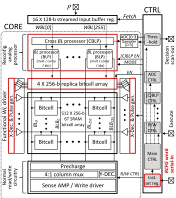
This common algorithmic ow is mapped to four sub-blocks of DIMA architecture corre-sponding to following processing stages: (1) multi-row functional read (FR) for fetching data D, (2) BL processing (BLP) for SD computations, (3) cross BL processing (CBLP) for
the aggregation of SD results, and (4) ADC and residual digital logic (RDL) for realizing thresholding decision function f( ).
The conventional digital architecture (Fig. 2.2(a)) and DIMA [3537,39] (Fig. 2.2(b)) both employ identical BCAs to storeDand an input buer to store streamedP. A key dierence
being, in DIMA, Ncol analog SD computations are embedded next to the BLs via BLPs,
× × × +
···
1/N···
f( ) (a)Algorithm Vector distance Scalar
distance f( ) SVM Dot product Multiplication sign
TM Manhattan distance Absolute difference min k-NN Manhattan distance Absolute difference majority vote MF Dot product Multiplication max
(b)
Figure 2.1: Functional ow of inference algorithms: (a) functional diagram, and (b) operations for each algorithm.
R ow de code r R ow d ec o de r
Digital processor Decision ( )
K-b bus d0
WL
driver Precharge
SA SA SA
Mux & buffer Memory
L:1
col. mux col. muxL:1 col. muxL:1
Input buffer ( ) d1 d2 d3 … … (a) FR r ow de code r FR r ow de code r ADC & RDL BLP SA SA SA
Mux & buffer
K-b bus Input buffer ( ) Cross BLprocessor (CBLP) Decision ( ) BLP BLP BLP BLP L:1
col. mux col. muxL:1
d0 d1 d2 d3 BLP L:1 col. mux Precharge WL driver (b)
Figure 2.2: Inference architecture (red marked drivers: turned-on wordline (WL) drivers at a time): (a) conventional system, and (b) deep in-memory accelerator (DIMA).
Table 2.1: DIMA vs. conventional architecture (withNcol ×Nrow bitcell array). Attribute Conventional DIMA
data storage
pattern row major column major column mux ratio fetched words per access BLswing/LSB ( ) 250 – 300 mV 5 – 30 mV # of rows per access 1
WL driver fixed pulse width
pulse width/amp modulated
In this way, DIMA can bypass the column muxing requirements imposed on conventional SRAMs. Furthermore, DIMA can directly aggregate the outputs of BLPs by CBLP to generate a VD. Thus, the nal output of the analog section in DIMA is a VD instead of data bits as in the case of a digital architecture. These dierences are summarized in Table 2.1 and described as follows:
Storage pattern: DIMA stores B bits of D in a column-major format vs. row-major
used in the digital architecture (Fig. 2.3(a)).
Read access: per BL precharge (read cycle), DIMA reads a function of B rows or a
word-row vs. a single row in the conventional architecture. This process, referred to as multi-row functional read (FR), generates a BL voltage drop ∆VBL proportional to
a weighted sum of the B bits per column [35] by using pulse-width modulated (PWM)
(Fig. 2.3(b)) or pulse amplitude modulated (PAM) WL signals [40, 41]. Thus, DIMA needs many fewer precharge cycles to read the same number of bits and this leads to both energy and throughput gains. However, in exchange, DIMA relaxes the delity of its reads as long as these fall within the error tolerance of the ML algorithm. Column muxing: unlike standard SRAMs which require an L : 1 column mux ratio
(typical L = 4 to 32) to accommodate a large-area sense amplier (SA) as shown in
dimen-sion is matched to the column pitch of the BCA. Column muxing limits the number of bits per access to Ncol/Lin standard SRAM compared to NcolB in FR.
Data reduction and decision: while the conventional architecture computes in digital processor, DIMA implements SD and VD via BLP and CBLP right next to the BCA using charge-based analog circuits. An ADC is used to digitize the analog CBLP output and pass it on to the RDL to compute f( ) in Fig. 2.2(b). This ADC operates
once per 128-256 SD computations.
Accuracy vs. energy: DIMA computations necessarily have a lower signal-to-noise ratio (SNR) than the computations in the digital architecture. This loss in SNR arises from the spatial transistor threshold voltage variations in the BCA which aect the FR process, and due to severe area-constraints on the BLP and CBLP. However, the SNR can be tuned to a level required by the ML algorithm by adjusting the BL swing
∆VBL.
In summary, the key to DIMA's speed-up and energy advantages over a digital architecture arises from its ability to read NcolB bits per access by FR, bypassing the column mux, and
via low-swing analog processing. The detailed operations of circuit and architecture in FR, BLP and CBLP stages are described in the following sections.
2.2 DIMA Design Principles
This section explains DIMA design principles based on SNR budgeting. The ML algorithms have inherent error resiliency due to following reasons: (1) the thresholding operation into xed number of classes provides an algorithmic noise margin as small errors do not change the classication results, and (2) the aggregation of a large number of elements, widely used for the dimensionality reduction in ML algorithms, makes the system insensitive to component noise.
The inherent noise immunity can be exploited to achieve aggressive energy and throughput benets for hardware implementations. Traditionally, supply voltage scaling has been widely
w o rd r o w ( B ro w s )
SRAM array (
)
SRAM array (
)
L:1 L:1 L:1 SA SA SA 1 0 1 e.g. 15 93 19 4 5 6 3 7911 e.g. 1-bit digitalbits fetched per access
bits fetched per access
word MSB T LSB T ∆VBL: B-bit analog ∆VBL: 1-bit analog
Normal read
Functional read (FR)
T
3 (a)Normal read
Functional read (FR)
(b)
Figure 2.3: Comparing conventional read and DIMA multi-row functional read (FR) operations: (a) fetched data, where B = 4 and L= 4 assumed, and red marked bitcells
Read + × Read + × Read + × +
···
SA[ -1:0]···
···
···
threshold 1/N SA[ -1:0] SA[ -1:0]···
(a) FR BLP + + FR BLP + + FR + BLP + + 1/N CBLP···
···
···
···
···
threshold analog processing (b)Figure 2.4: Functional ow of inference system: (a) conventional system, and (b) DIMA system.
employed to achieve energy eciency, but at the cost of signicantly degraded throughput (e.g., quadratically degraded to voltage scaling [42]). Moreover, the error tends to happen at MSB in digital processors due to the carry ripple behavior in arithmetic operations [43]. Another potential approach to exploit the ML's error immunity is reducing the ∆VBL to
save memory read energy. However, the conventional architecture with separated memory and processor does not allow enough ∆VBL scaling. This is because the ∆VBL needs to
be converted to full swing to be processed in digital logic through SA, which acts as bit-wise early decisions (Fig. 2.4(a)). If early decision errors happen at MSB due to η1,2,...,N by
∆VBLscaling, the error magnitude can increase beyond application's error immunity, leading
+ +
+ +
Early decision Delayed decision threshold (a)
SNR [dB]
B it e rr o r p ro b ab ili ty pe (b)Figure 2.5: Delayed vs. early decision scenarios: (a) simplied functional ow with
x and xˆ∈ {1,−1}, and (b) bit error probability pe vs. SNR.
< 10dB with MSB error [30, 31]). Being aware of this issue, several low-power SRAM techniques [30, 31] were proposed for inference applications with selective MSB protection achieving limited (35%) energy savings in the memory, but not in the processor.
To resolve these issues, DIMA eliminates the separation between the low-swing memory and high-swing processor, but budgets SNR by employing aggressively low-swing operations in both memory and process jointly (Fig. 2.4(b)). This is enabled by employing the FR, which implicitly performs D/A conversion, and subsequent mixed-signal BLP and CBLP processings. Despite degraded SNR, the system level robustness of DIMA is maintained
by following three principles: (1) delayed decision, (2) non-uniform bit protection, and (3) aggregation.
2.2.1 Delayed Decision
Due to the absence of SAs between memory and processor, DIMA does not require early decision right after BL discharge where noise ηa1 is added, but hard decision (thresholding) happens only at the end of classication process (Fig. 2.4(b)), namely delayed decision. In this section, early and delayed decisions are compared with a simple example of binary bit transmission (x∈ {1,−1}) in Fig. 2.5(a), where noise distributionη1,2 ∼ N(0, σn2), threshold
level 0, and equal prior P(X = 1) = P(X = −1) = 0.5 are assumed. The bit error
probabilities pe, assuming identical independent noise sources, can be derived as follows:
pe = 2Q(σ1 n)[1−Q( 1
σn)] for early decision
Q(√1
2σn) for delayed decision
(2.1)
Figure 2.5(b) showspe behavior with respect to the SNR based on (2.1). It is clearly shown
that the delayed decision is more robust in a low-SNR regime as the early decision tends to amplify noise contribution in the regime. In this sense, the delayed decision improves the robustness of DIMA, where the SNR is tightly budgeted.
2.2.2 Non-Uniform Bit Protection
The FR with PWAM (Fig. 2.2(b)) allows us to assign voltage swing unequally based on the signicance of information (bit positions), namely non-uniform bit protection. When the total swing ∆VBL is budgeted for multi-row reading of B bits, the swing assigned for the
∆Vn=
∆VBL/B for uniform bit protection
∆VBL2n−1/(2B−1) for non-uniform bit protection
(2.2)
For example, the non-uniform bit protection gives roughly 2.1× more swing for MSB and
3.8× less swing for LSB compared to uniform bit protection when B = 4. In this way,
the limited resource (voltage swing) is more eciently budgeted in the DIMA to reduce the errors in more signicant bit positions and thus improve application level robustness.
2.2.3 Aggregation
The charge-sharing process in the CBLP eciently averages out noise contributions by re-ducing the standard deviation of output by √N times after aggregating N independent
mean-zero random noise sources in Fig. 2.4(b). Specically, the DIMA's CBLP is eective in averaging out the noise in the SD computations as the error statistics of noise in the analog circuitry closely follows independent mean-zero behavior (e.g., spatial threshold vari-ation). Moreover, DIMA provides the average-out opportunity for both ηa1 and ηa2 before the thresholding due to the delayed decision whereas the conventional digital architecture goes through the early decision before having the aggregation opportunity.
2.2.4 Measured Result
This section proves the eectiveness of the above mentioned principles based on measurement results of a prototype IC in a 65 nm CMOS process, which is described in more detail in Chapter 3. Figure 2.6(a) shows bit error rate (BER) measured by fetching 16 KB via the conventional SRAM read and the energy trend by scaling ∆VBL. The measured BER is
0 0.1 0.2 0.3 0.4 0.5 0.6 0 100 200 300 B it e rr o r ra te (B ER ) ∆VBL[mV] (a) 0 0.2 0.4 0.6 0.8 1 30 60 100 138 180 230 280 350 P ro b ab il it y o f d e te ct io n ( Pde t ) ∆VBL,avg [mV] Conventional simulated (w/ BER measured from IC) DIMA IC measured
(b)
Figure 2.6: Bit error rate (BER) vs. ∆VBL vs. application accuracy (face detection with
SVM) in conventional system: (a) BER of normal SRAM read operation measured from prototype IC, and (b) application accuracy obtained by simulating a conventional system with measured BER with measured DIMA accuracy.
application level accuracy in Fig. 2.6(b), where ∆VBL,avg is the average BL voltage swing
assigned per bit for a fair comparison of two systems. The DIMA's FR fetches B-bits
with single BL swing ∆VBL whereas conventional memory reads a single bit, leading to the
following denition of ∆VBL,avg:
∆VBL,avg =
∆VBL for conventional memory
∆VBL/B for DIMA
The setup for SVM including data set and image size is described in Chapter 3. It is shown that 0.7% BER at ∆VBL = 230 mV can cause 4% degradation in detection accuracy
of the conventional system. On the other hand, DIMA's measured accuracy shows much more robustness with even lower ∆VBL,avg due to the above mentioned three principles.
Specically, the eective ∆VBL of conventional architecture is L times larger than those
shown in Fig. 2.6(b) as L BLs needs to be discharged to access only one of those through
column muxing. Thus, it can be concluded that the DIMA allows more aggressive ∆VBL
scaling compared to the conventional system, leading to signicant energy savings.
The following section focuses the realization of the above described system rationale and implementation challenges and solutions.
2.3 Functional Read (FR)
This section explains the FR stage in detail, which performs data access and simple SD computations. Two design techniques: (1) sub-ranged read, and (2) replica bitcell are in-troduced to enhance the linearity of FR and achieve ecient data writing, respectively. In addition, design principles for key parameters such as pulse widthT0 and amplitudeVW Lare
VWL0 d0 d1 CWL CWL VBL VPRE 6T SRAM bitcell VWL1 Prech 6T SRAM bitcell VWL0 VWL0 d0 d0 CBL CBL VBLB (a) T0 d3 d2 d1 d0 T1=2T0 T2=4T0 T3=8T0 ∆VBL(D) VBL VWL3 VWL2 VWL1 VWL0 8∆Vlsb 4∆Vlsb 2∆V lsb ∆V lsb (b)
Figure 2.7: Multi-row functional read (FR) using pulse width modulated access pulses [35]: (a) column structure and bitcell, and (b) waveforms during a 4-bit word (D= 0000b0)
read-out (WL pulses are sequentially applied for visibility, but can be overlapped).
2.3.1 FR Operation
The FR stage generates the bitline voltage drop∆VBL(D)proportional to the weighted sum
D = ΣBi=0−12idi of column-major stored data {d0, d1, ..., dB−1} (see Fig. 2.7(a)). The voltage drop ∆VBL(D)can be generated via a simultaneous application of PWAM access pulses to
multiple rows per precharge cycle. This is in contrast to the use of single-row xed width and amplitude pulses per precharge cycle in conventional SRAM read.
Consider FR of B rows using PWM [35] with binary-weighted pulse widths Ti ∝ 2i(i ∈
[0, B−1]) of VW L(i) as shown in Fig. 2.7(b) [35]. The charge ∆Qi(di) drawn from the BL
capacitance CBL is given by:
∆Qi(di) =diTiI(Ti) (2.3)
where I(t)is the current drawn by the ith bitcell. This current can be Taylor series
approx-imated as: I(t) = VP RE Ri e− t RiCBL ≈ VP RE Ri (1− t RiCBL )≈ VP RE Ri (2.4) provided t RiCBL. Substituting t = Ti into (2.4) and the resulting expression for I(Ti)
into (2.3), we obtain:
∆Q(di) = diTi
VP RE
Ri
(2.5) where Ti RiCBL. Therefore, the expression for the total BL voltage drop ∆VBL(D) can
be obtained as follows: ∆VBL(D) = PB−1 i=0 ∆Qi CBL = VP RE CBL B−1 X i=0 diTi Ri (2.6)
As the pulse widths are binary weighted Ti = 2iT0 where T0 is the LSB pulse width, and if
Ri =RBL, i.e., the discharge paths of all theB bitcells in a column have identical resistances,
then ∆VBL(D) = VP RE RBLCBL T0 B−1 X i=0 2idi = ∆Vlsb B−1 X i=0 2idi = ∆VlsbD (2.7)
where ∆Vlsb = RVP REBLCTBL0 , and D is the decimal value of the one's complement of D. The
expression in (2.7) is idealized as it assumes the following four conditions: 1. Ti RiCBL
2. Ti = 2iT0
3. Ri =RBL (no variation across rows)
4. RBL is a constant overVBL.
In practice, these conditions will not be fully met leading to a deviation, i.e., non-linearity, from (2.7), and spatial variations from one group ofB bits to another across the BCA. These
non-idealities and techniques to alleviate them will be described in Section 2.3.3.
A similar expression as (2.7) for ∆VBLB(D) can be obtained by replacing di with di in
(2.7). Thus, the FR stage converts the stored digital data D into bitline voltage drops
∆VBL(D) and ∆VBLB(D), i.e., the FR stage is a digital-to-analog converter. Additionally,
two B-bit words (D and P) stored dierent rows but in the same column. For example,
from (2.7), D+P is obtained by applying FR to rows containingD and P to obtain:
∆VBL(D+P) = ∆Vlsb(D+P) = B−1
X
i=0
2i(di+pi) (2.8)
Similarly, subtraction D−P can be realized by storing P (one's complement of P) in the
same column as D. Subtraction will be discussed in Section 2.4 in more detail.
2.3.2 Design Guidelines
The BL swing∆VBLgenerated by the FR stage is subject to the impact of spatial transistor
threshold voltage variations caused by random dopant uctuations [44], voltage-dependence of the discharge path (access and pull-down transistor in the bitcell) resistance RBL (see
(2.7)), and the nite transition (rise and fall) times of the PWM WL access pulses. These non-idealities can be incorporated into (2.7) as follows:
∆VBL(D) = ∆Vlsb B−1 X i=0 2id i(1 +γi) (1 +ρi(VBL) +δi) (2.9)
where δi is a random variable describing the the impact of spatial transistor threshold
volt-age variations on the discharge path resistance RBL aecting Condition 3 (Ri = RBL) in
Section 2.3.1,ρi(VBL)is a variable that captures the impact of the BL voltage-dependence of
RBL which aects Condition 4 (RBLshould be a constant), andγi is a deterministic variable
that captures the impact of nite transition times on the pulse widthsTi aecting Condition
2 (Ti = 2iT0), with the aect on the LSB pulse widthT0 being most severe.
The presence of δi, ρi, and γi imposes certain design constraints in order to alleviate
their impact so that (2.9) approaches the ideal expression in (2.7). For example, ρi can
be reduced by ensuring that the access transistor in the discharge path does not transit from saturation into the triode region to satisfy Condition 4. This can be achieved by lowering the WL access pulse amplitude VW L, which has the additional benet that RBL is
Similarly, the impact of γi can be alleviated by ensuring that the design parameter T0 is lower bounded as T0 > Tmin so that the rise (Tr) and fall (Tf) times of VW L are a small
fraction, e.g., Tr+Tf <0.5Tmin, of T0 and hence Condition 2 (Ti = 2iT0) can be met. That and Condition 1 implies thatTmin < T0 < Tmax. Lastly,δi can be alleviated by ensuring that
VW L is suciently large so that variations inRi are reduced, i.e., Condition 3 (Ri =RBL) is
approximated well. This lower bound onVW L can be relaxed as DIMA's aggregation process
in the CBLP compensates for the impact of δi. However, VW L does have an upper bound
to avoid destructive read operation, e.g., VW L <0.8VP RE. Hence, for the prototype IC, we
chose VW L = 0.65VP RE. Note that it is possible to pre-distort the data stored in the BCA
in order to alleviate the impact of deterministic errors ρi and γi.
The worst-case values ofρi andγi are estimated to be less than 41% and 37%, respectively,
as estimated from measured results of the multi-functional 65 nm CMOS prototype IC. Monte Carlo post-layout simulations of the BCA shows that the impact ofδi leads to a 12%
variation (σ/µ) in∆VBL(D) for typical values ofVW L = 0.65 V, VP RE = 1 V, T0 = 250 ps,
N = 128, B = 8, and Nrow = 512. Section 3.3.3 indicates that these non-idealities have a
negligible impact on inference accuracy for the data sets being considered in this work.
2.3.3 Design Techniques
We present two design techniques to overcome the design constraints described in Sec-tion 2.3.2.
• Sub-ranged Read: Realizing a highly linear FR stage when B > 4 bits is challenging
because the constraintTmin = 2(Tr+Tf)< T0 < Tmax 21−BRBLCBL is hard to meet. For
example, T0 <125 ps when B = 5 and T4 = 2 ns. This value of T0 is hard is achieve when driving high WL capacitance (e.g., 200 fF) with a row pitch-matched wordline driver. The sub-ranged read technique solves this problem as described next.
In sub-ranged read [39], theB/2MSBs representing dataDM andB/2LSBs representing
dataDLare stored in adjacent columns of the BCA as shown in see Fig. 2.8(a). For example,
when B = 8, DM = 8d7 + 4d6+ 2d5 +d4 and DL = 8d3 + 4d2 + 2d1+d0. Three switches
d7 d6 d5 d4 VBLM(DM) d3 d2 d1 d0 VBLL(DL) ø1 ø2 ø3 BLPM BLPL VBL(D) (a) CBLP CBL
ø2
VBLM(DM)ø1
CBLø3
CBLP Ctune VBLL(DL) CM CL=(1/16)CM VBL(D) (b)Figure 2.8: Sub-ranged read with B = 8: (a) BL pair structure (two neighboring bitcell
columns), and (b) equivalent capacitance model [39], where DM = 8d7+ 4d6+ 2d5+d4 and DL= 8d3+ 4d2+ 2d1+d0.
Ctuneenables the realization of a predened capacitance ratio (16 : 1 forB = 8) between the
MSB and LSB BLs' capacitances CM and CL, respectively. This ratio is needed to weigh
the voltage drop on the MSB BL (∆VBLM) by a factor of 2 B
2 more as compared to the
voltage drop on the LSB BL (∆VBLL). The desired capacitance ratio is obtained by setting
CM = CBL +CBLP +Ctune and CL = CBLP as shown in Fig. 2.8(b), and varying Ctune
modies CM so as to realize CM :CL= 2 B
2 : 1.
The sub-ranged read proceeds as follows:
1. the FR process is simultaneously applied to the MSB and LSB columns withφ1,2,3 = 0 (all open) thereby generating voltage drops∆VBLM(DM)and∆VBLL(DL), respectively.
2. the switchφ1 is closed so that the voltage∆VBLM(DM)is developed acrossCM. Switch
φ2 is pulsed to generate the voltage ∆VBLL(DL) onCL.
3. the switch φ3 is closed to generate the voltage drop at the nal output
∆VBL(D) = 1 CM +CL [CM∆VBLM(DM) +CL∆VBLL(DL)] (2.10) = 1 2B2 + 1 h 2B2∆V BLM(DM) + ∆VBLL(DL) i (2.11)
VBL d0 d1 d2 d3 VWL0 VWL1 VWL2 VWL3 p0 p1 p2 p3 VWLP0 VWLP1 VWLP2 VWLP3 W B L WWL3 WWL2 WWL1 WWL0 VBLB Replica BCA Normal BCA WWL0 WWL3 WWL2 WWL1 VWLP3 p3 p3 WWL3 WWL3 W B L B L B LB Replica bitcell VWLP3 (a) WBL p0 p1 WWL0 WWL1 0 p2 p3 0 WWL2 WWL3 (b)
Figure 2.9: Replica BCA: (a) bitcell column (B =4), and (b) timing diagram for replica
BCA writing [39].
Thus, for B = 8, the voltage drop ∆VBLM(DM) is weighted 16× more than ∆VBLL(DL) to
obtain the voltage drop ∆VBL(D)which is proportional to 16DM +DL.
•FR Replica BCA: As described in Section 2.3.1, two operands D and P are required to
implements various SD computations. For example, in order to realize the dierenceD−P
(see (2.8)), P is stored in the same column as D but in a dierent row. Typically, P is a
streamed in data, e.g., a template in template matching or image pixels. Storing P in the
same BCA as D will require repeated SRAM write operations which incurs large energy
and delay costs as these require full BL swing. This problem can be solved via the use of a replica BCA as described next.
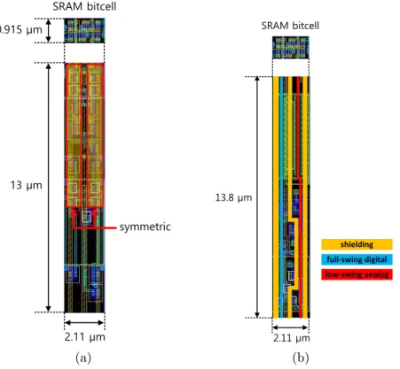
SRAM bitcell 0.915 μm 13 μm 2.11 μm symmetric (a) SRAM bitcell 2.11 μm 13.8 μm shielding full-swing digital low-swing analog (b)
Figure 2.10: Pitch-matched layouts of BLP blocks relative to a SRAM bitcell: (a) analog comparator, and (b) a part (1/5) of charge redistribution-based multiplier.
The replica BCA (Fig. 2.9(a)) enables fast writes ofP via separate write BL (WBL) and
WL (WWL) [39]. Thus, P can be written into the replica BCA column by providing data
in a bit-serial manner via the WBL (Fig. 2.9(b)) while disabling the cross-coupled inverter feedback loop in the replica bitcell via W W L. During a subsequent FR, the replica BCA
behaves as an extension of the regular BCA. The layout of replica bitcell needs to be similar to normal bitcell to have the same discharge strength except the needs of WBL and WWL circuitry.
2.4 Bitline Processing (BLP) and Cross BLP (CBLP)
This section describes BLP and CBLP stages, which perform various SD computations and aggregation, respectively. The BLP and CBLP operations rely on tightly pitch-matched analog processing (see Fig. 2.10) resulting in many implementation challenges. Thus, design
principles for key parameters are presented based on the analysis of various noise sources such as charge injection, thermal noise, and coupling noise.
2.4.1 BLP Operation
The Ncol BLP block in Fig. 2.2(a) accepts two operands: (1) its corresponding bitline
voltage drop ∆VBL(D)generated via the FR stage, and (2) a word P to generate an output
voltage VB(D, P). The BLP block needs to be re-congurable in order to support multiple
SD computations required by various ML algorithms. Furthermore, the BLP block layout needs to be column-pitch matched to the BCA. Thus, the BLP stage is a massively parallel analog SIMD processor.
Next, we describe how SD functions such as absolute dierence |D −P| [35] and mul-tiplication DP [36] can be implemented in the BLP. These SD functions are required to
compute commonly used VDs: Manhattan distance (MD) (PN
i=1|Di−Pi|) and dot product (DP) (PN
i=1DiPi).
2.4.1.1 Absolute Dierence
The absolute dierence |D−P|can be written as [35]:
|D−P|=max(D−P, P −D) (2.12)
From (2.8), the bitline voltage drop corresponding to the dierence D−P is obtained as:
∆VBL(D−P) = ∆Vlsb(D+P) (2.13)
The intrinsically dierential structure of the SRAM bitcell enables one to evaluatemax(VBL, VBLB),
i.e., the voltages on the BL and BLB, quite easily via the use of a local BL compare-select as shown in Fig. 2.11(a). Thus, from (2.12) and (2.13), we get
VWL1 VWL2 VWL3 VWL0 M R -F R o f D M R -F R o f P VWL(x+1) VWL(x+2) VWL(x+3) VWL(x+0) EN VBL + -0 1 COMP OUT EN MUX VB 6T SRAM bitcell EN VWL0 VWL1 6T SRAM bitcell VBLB (a) C C C ø3,2 ødump ø3,1 VPRE C ø3,3 C ø3,0 ødump ødump ødump ødump VPRE VPRE VPRE VPRE VB ø2,X ø2,0 (p0) ø2,1 (p1) ø2,2 (p2) ø2,3 (p3) ødump ø2,X ø2,0 ø2,1 ø2,2 ø2,3 ø3,0 ø3,1 ø3,2 ø3,3 VBLB(D) if p0=0 if p1=0 if p2=0 if p3=0 (b)
Figure 2.11: Bitline processing (BLP): (a) absolute dierence, where Dand P are stored in
max(VBL, VBLB) = max(VP RE−∆Vlsb(P +D), VP RE−∆Vlsb(D+P))
=max(VP RE−∆Vlsb(P + 2B−1−D), VP RE−∆Vlsb(D+ 2B−1−P))
=VP RE−(2B−1)∆Vlsb+ ∆Vlsbmax(P −D, D−P) (2.14)
Thus, applying FR to D and P simultaneously results in VBL and VBLB being proportional
toP−DandD−P, respectively. The local BL compare-select block (Fig. 2.11(a)) provides
the maximum of VBL and VBLB, and hence the absolute dierence |D−P|.
2.4.1.2 Multiplication
Figure 2.11(b) shows a charge redistribution-based mixed-signal multiplier with inputs∆VBLB(D)
(FR stage output) and an externally provided B-bit digital word P, whose bits pi control
the φ2,i switches. The multiplier output voltage VB is given by:
VB(D, P) =VB(DP) = VP RE−(0.5)BP∆VBLB(D) = VP RE−(0.5)B∆VlsbDP (2.15)
Thus, voltage drop∆VB(DP) = VP RE−VB(DP)∝DP represents the product ofD andP.
Note that, the multiplier employs unit size (25 fF) capacitors rather than binary-weighted ones as in [45], due to stringent column pitch-match constraints on the BLP.
The timing diagram in Fig. 2.11(b) describes the operation of the multiplier, which is also summarized below:
rst, the unit capacitors are charged to ∆VBLB(D) by pulsing the φdump switches.
then, the switch φ2,i is pulsed only ifpi = 0thereby charging the capacitor
correspond-ing to i-th bit VP RE. The capacitors corresponding to pi = 1 retain the voltage equal
to∆VBLB(D).
nally, the switches φ3,i are pulsed sequentially starting fromφ3,0, φ3,1. . . φ3,B−1. This leads to charge sharing between adjacent capacitors.
ø1 ø2 CS ø2 VB(D1,P1) VB(D2,P2) CS ø1 VC VB(DN,PN) CS ø1 ø2
Figure 2.12: Cross bitline processing (CBLP).
Note that when φ3,k (k = 0, . . . , B−1) is pulsed, the two charge sharing capacitors settle to
a voltage of:
VP RE −(0.5)k+1(2kpk+...+ 2p1+p0)∆VBLB(D) (2.16)
thereby realizing (2.15) when k =B−1.
2.4.2 Cross Bitline Processing (CBLP), ADC, and Residual Digital Logic
(RDL)
The cross BL processor (CBLP) (Fig. 2.12) samples the output voltage (VB(D, P)) of the
BLP on the BL-wise sampling capacitors CS at each column by pulsing the φ1 switches. Next the φ2 switches are pulsed to generate the CBLP output VC in one step. In this way,
CBLP implements dimensionality reduction, which is a widely used function in inference algorithms. Finally, the CBLP output VC is converted to the digital domain by the ADC
to be stored or further processed by the RDL. The RDL implements slicing/thresholding functions such as min, max, sign, sigmoid, and majority vote. Note that the ADC and RDL need to process one scalar value (VC) generated from a massively parallel (> 128) SD
2.4.3 Design Guidelines
The BLP can be congured to compute the absolute dierence |D−P| (MD mode) or the scalar product DP (DP mode).
The dominant source of non-ideality in computing|D−P|is due to the comparator oset in the compare-select block (see Fig. 2.11(a)). However, this input oset aects the BLP output VB minimally. This is because the input oset aects the output only when VBL
and VBLB are close to each other. Thus, the BLP output VB =max(VBL, VBLB)in (2.12) is
supposed to have an error of only small magnitude|VBL−VBLB|. Additionally, the error inVB
being uncorrelated across the columns gets averaged out further by the CBLP. The column pitch-matched comparator layout shown in Fig. 2.10(a) is constrained to be symmetric to minimize the input oset. Monte Carlo post-layout simulations in the 65 nm CMOS process indicates that the input oset follows the distribution N(0,(10mV)2).
Computation of the product DP in the BLP (see Fig. 2.11(b)) and summation in the
CBLP (see Fig. 2.12) is done via charge redistribution circuits. These circuits suer from multiple noise sources: (1) charge-injection noise, (2) coupling noise, and (3) thermal noise. Assuming a junction capacitance of 0.05 fF [46] using minimum sized switches, we nd that storage capacitanceC needs to be larger than 13 fF in order to ensure 8-b output precision.
The 8-b precision in a swing of300mV results in a resolution ofVres= 1mV. Hence, thermal
noise considerations (p
KT /C <0.5Vres) lead to the requirement of C >17 fF atT = 300
K. Hence, we chose C = 25 fF to provide sucient design margin.
Due to the tight pitch-matching constraints, digital signals need to be routed over analog nodes in the BLP and CBLP generating signicant coupling noise. In order to alleviate coupling noise, low-swing analog nodes were shielded from the digital full-swing lines as shown in Fig. 2.10(b).
2.5 Models for Circuit Non-Ideal Behavior, Energy, and Delay
1 The analog-intensive DIMA operation is subject to a number of circuit-level non-idealities [35]. This section presents comprehensive behavioral models of dominant non-idealities in each analog signal processing step for the prediction of application accuracy. Energy and delay models are also provided as a function of major design parameters.The major non-idealities are as follows:
(a) non-linearity of the FR process due to the voltage-dependent resistance of BL discharge path
(b) local transistor threshold voltage Vth-mismatch across bitcells caused by random
dopant uctuations
(c) non-ideal sub-ranged read due to the inaccuracy of capacitance ratio between the MSB and LSB columns
(d) input oset of the analog comparator
This section focuses on Manhattan distance (MD) to analyze a variety of noise sources. A similar analysis can be applied to the other VD kernels.
2.5.1 Circuit-Aware Behavioral Model
2.5.1.1 FR with Subtraction (summation)
The FR for MD computation is simulated with HSPICE and the non-linearity is modeled by a polynomial equation given by:
∆VBL0 (D, P) =c2(D+P)2+c1(D+P) +c0 (2.17) where ∆VBL0 (D, P) is a distorted version of ∆VBL(D, P), and the tting parameter c0, c1, and c2 depend upon RBL, CBL, T0, the process parameters including Vth, carrier mobility,
saturation carrier velocity, and the channel length modulation parameter. The expressions
1This section is adopted from M. Kang, M.-S. Keel, N. R. Shanbhag, S. Eilert, and K. Curewitz, An
energy-ecient VLSI architecture for pattern recognition via deep embedding of computation in SRAM, in 39th IEEE International Conference on Acoustics, Speech and Signal Processing (ICASSP). © 2014 IEEE
for∆VBLB0 (D, P)can be obtained by substitutingP andP in (2.17) withDand D,
respec-tively.
2.5.1.2 Variation of FR
The impact of Vth-mismatch is modeled as Gaussian distributed random variables as shown
below:
∆VbBL(D, P)∼ N(∆VBL0 (D, P), σ24V
BL(D,P)) (2.18)
where σ2
4VBL(D,P) is the variance of ∆VbBL(D, P)due to Vth-mismatch across bitcells.
The variance σ42V
BL(D,P) is expressed as follows by assuming that the BL voltage drop
from reading D and P are independent:
σ42V BL(D,P)=σ 2 4VBL(D)+σ 2 4VBL(P) (2.19)
Furthermore, the voltage drop by FR ofDcan be modeled as an addition of binary scaled B independent Gaussian random variables when sub-ranged read is employed for every B
bits. Thus, the varianceσ2
4VBL(D) can be expressed by:
σ42V
BL(D) = {(2 B−1
dB−1)2+...+ (22d2)2+ (2d1)2+ (d0)2} ×σ42VBLB(D=1) (2.20)
The σ2
4VBL(P) can be achieved by replacing the di in (2.20) intopi.
2.5.1.3 Sub-Ranged Read
The parasitic capacitance ratio between BLM and BLL needs to be M(= 2B/2) : 1 for the sub-ranged read as shown in (2.10). Inaccuracy of the ratio (M : 1) causes a non-ideality,
b VBL(D, P) = M M+ 1[{VP RE−∆VbBLM(DM, PM)} +{VP RE−∆VbBLL(DL, PL)}/M] (2.21) 2.5.1.4 Absolute Operation
The non-ideal BLP output VbB,j from the j-th column in DIMA is expressed with the ideal
valueVB,j as follows: b VB,j =g1{QVbBL(Dj, Pj) +QVbBLB(Dj, Pj)}+g0 (2.22) Q= 1 ifVbBL(Dj, Pj)>VbBLB(Dj, Pj) +VOS 0 otherwise
whereVOS ∼ N(0, σ2comp)is input oset voltage of the comparator which is modeled as a zero
mean Gaussian random variable with variance σ2
comp. Coecients g0 and g1 model voltage change due to the charge sharing between the BL and sampling capacitor, and leakage current.
2.5.1.5 Sampling and Capacitive Addition
The thermal noise in the sampling capacitor is negligibly small as compared to other noise sources by employing capacitors larger than 10f F. The non-ideal CBLP output (Vb) from
charge sharing N sampling capacitances can be modeled as follows:
b VC = 1 N N X j=1 b VB,j (2.23)
2.5.2 Throughput Model
The throughput of conventional systems is limited by the memory access delay in memory-intensive algorithms. In such applications, throughput improvement factor S by the DIMA
can be expressed as follows: S = 1 2(LB)( Tconv TDIM A ) (2.24)
where theTconv is the cycle time for single read access of conventional system, and TDIM A is
the sum of the delays of FR, BLP, and CBLP. The TDIM A is generally larger than Tconv as
DIMA accesses multiple rows to fetch a vertically stored word and complete the following analog operations. The scaling factor B is due to the FR process reading B rows per
access. In addition, the DIMA bypasses the L : 1 column mux resulting in scaling factor
L. The scaling factor 12 occurs because the sub-ranged read reduces eective throughput.
Hence, higher throughputs (S = 3.2 ∼12.8) can be easily achieved, e.g., by setting B = 8,
L= 4, 8, 16, and TDIM A= 5Tconv.
2.5.3 Energy Model
The energy consumptions of DIMA and conventional architecture per read operation and following processing of a B-bit word for MD computation are modeled, respectively, as
follows:
Econv = BLCBL∆VBLVP RE +BESA+Eleak+Elogic (2.25)
EDIM A = 4CBL(∆VBL)VP RE+Ecomp+Eleak/S+EBLP (2.26)
The energy eciency of DIMA can be evaluated by comparing (2.25) and (2.26). The energy component Elogic in (2.25) corresponds to EBLP in (2.26). The Ecomp in (2.26) is
the energy for an analog comparator, and this is almost the same as the sense amplier energyESA in (2.25). The rst term in (2.26) does not have the scaling factor ofLas DIMA
terms of (2.26) because the FR processes a B-bit word per single BL discharge. However,
the scaling factor of four is created in the rst term of (2.26) to read not only D but also P and employ the sub-ranged read. Energy savings can be observed by comparing the rst
and second terms becauseLB ranges from 32 to 128 whenB = 8. It is assumed that a
deep-sleep mode is enabled during standby using techniques such as power gating or lowering the
VDD for the BCA [4749]. Therefore, Eleak = PleakTconv, where Pleak is the leakage power
consumption. The DIMA's intrinsically parallel operation makes its eective read cycle time smaller by a speed-up factor ofS (S >3), therefore the leakage energy is also reduced. The
EBLP is smaller than the Elogic due to a low-swing signal processing.
2.5.4 Prediction of Application Accuracies
In this section, the application accuracy is predicted in terms of probability of detection (PDET) as a function of major design parameters based on the behavioral models described
in the previous sections.
The decision of pattern matching with the DIMA based on distance metrics can be rep-resented as follows:
uopt_DIM A = arg min
u {f(u) +ηu, u= 1, ..., U} (2.27)
whereuopt_DIM A is the decision from DIMA to nd the index of the candidate with minimum
distance. The f(·) is a error-free distance metric, U is the number of candidates, and ηus
are independent random variables representing noise due to the non-idealities of FR, BLP, and BLP for theu-th candidate. The PDET of DIMA can be dened as follows:
PDET = Pr{uopt=uopt_DIM A} (2.28)
= Pr{f(uopt_DIM A) +ηuopt_DIM A < f(u) +ηu, u= 1, ..., U}
where uopt is the correct index of the candidate with minimum distance. The circuit-aware
applica-tion level accuracy. In this secapplica-tion, the only local transistor Vth-mismatch across bitcells is
considered as the only source of non-ideality in DIMA as it is the dominant source of error. Equation (2.21) can be expressed with an error-free ideal BL voltages as follows:
ˆ VBL(D, P) = VP RE− M M + 1 ∆VBLM(DM, PM) − 1 M + 1 ∆VBLL(DL, PL) +η∆VBL = VBL(D, P) +η∆VBL (2.29)
where η∆VBLB is additive Gaussian noise with mean zero and variance described by:
σ∆2V BL(D,P) = M2 (M+ 1)2σ 2 ∆VBL(DM,PM)+ 1 (M + 1)2σ 2 ∆VBL(DL,PL) (2.30)
Similarly, VˆBL(D, P) can be denoted as follows:
ˆ
VBL(D, P) =VBL(D, P) +η∆VBL (2.31)
The non-ideal BLP outputVˆB,j(D, P)in (2.22) can be described with equivalent additive
noise ηB,j as follows, but neglecting the comparator oset for simplicity:
ˆ
VB,j = g1max{VBL(Dj, Pj) +η∆VBL(Dj,Pj), VBLB(Dj, Pj) +η∆VBLB(Dj,Pj)}+g0
= VB,j+ηB,j (2.32)
where VB,j = g1max{VBL(Dj, Pj), VBLB(Dj, Pj)}+g0, which is an error-free BLP output. The ηB,j is not a Gaussian random variable due to the maximum operation althoughη∆VBL
and η∆VBLB are independent Gaussian random variables [50]. However, the mean and
vari-ance of ηB,j can be expressed as follows [51]:
V ar[ ˆVB,j] = g12(µ21+σ21)Φ(α) +g12(µ22+σ22)Φ(−α) +g12a(µ1+µ2)φ(α)−(E[ ˆVB,j])2 (2.34) where µ1=VBL(Dj, Pj); µ2=VBLB(Dj, Pj); σ21 =σ2∆VBL(D,P); σ 2 2 =σ∆2VBLB(D,P); a2=σ∆2V BL(D,P)+σ 2 ∆VBLB(D,P), α= VBL(Dj, Pj)−VBLB(Dj, Pj) a
where φ(x) and Φ(x) are the Gaussian probability density function and cumulative density
function, respectively.
The VˆB,j in (2.23) can be substituted by (2.32) as follows:
ˆ
VC = VC+ηC (2.35)
where VC = N1 PNj=1VB,j and ηC = N1 PNj=1ηB,j are equivalent additive noise present in
VC. Although ηB,j is not a Gaussian random variable, the distribution of ηC approaches
a Gaussian distribution N(E[ηC], V ar[ηC]) asL increases by the central limit theorem [50]
with the following mean and variance:
E[ηC] = 1 N N X j=1 E[ ˆVB,j]−VC V ar[ηC] = 1 N2 N X j=1 V ar[ ˆVB,j] (2.36)
Now (2.28) can be expressed withηC, and the PDET is given by:
where error-free MD computation kernel f(·) can be expressed as follows: f(u) = 1 L L X j=1
[g1max{VBLB(Du,j, Pj), VBL(Du,j, Pj)}+g0] (2.38)
For simplicity, the probability that everyf(u) +ηC,u in (2.37) is larger than constant value
x is dened by: h(x) = Y u6=uopt Pr{x < f(u) +ηC,u} (2.39) = Y u6=uopt Q x−(pf(u) +E[ηC,u]) V ar[ηC,u] !
where x ranges from 0 to 1 as the voltage level of CBLP output cannot be less than 0 and
higher than VDD = 1.
Thef(uopt) +ηC,uopt in (2.37) is a random variable whereasx in (2.39) is a constant value.
Thus,h(x)is integrated with probability density function of f(uopt) +ηC,uopt over the entire
dynamic voltage range as follows:
PDET =
Z 1
x=0
h(x)φ x−(fp(uopt) +E[ηC,uopt]) V ar[ηC,uopt]
!
dx (2.40)
2.5.5 Simulation Results
This section provides validation of behavioral models from (2.17) to (2.23) by HSPICE Monte-Carlo simulations in a 65 nm CMOS process technology. Then, PDET of practical
application is obtained via Monte-Carlo simulations using the validated behavioral mod-els. Finally, the PDETs from Monte-Carlo system simulations are compared with the PDET
Table 2.2: Design and model parameters in (2.17)-(2.23). Parameter Values Parameter Values
VDD 1 V VW L 0.4 - 0.9 V VP RE 1 V L 4, 8, 16 array size 256×512 N 2 - 256 T0 300 ps M 16 B 8 CLK freq. 1 GHz σcomp 10 mV g0, g1 0.890, 0.086 σ4VBL/µ4VBL(D= 1) 6.4% c0 =−3.04×10⁻³,c1 = 0.037,c2 =−2.43×10⁻⁴ 2.5.5.1 System Congurations
Two banks with512×256BCA per bank are assumed to store a dataset ofDs. Bit precision
B = 8 is chosen for D and P, and sub-raged read is applied for every 4 bits as shown in
Fig. 2.8(a). The L is chosen to be 4, 8, and 16, which are the most widely used values. It
is assumed that ∆VBL(B) = 250 mV and VW L = 1 V in a conventional SRAM to achieve
sensing margin. A metal oxide metal (MOM) capacitor is used to implement the sampling capacitor in order to balance leakage reduction and area eciency. The analog comparator is sized to t in the horizontal dimension of the SRAM bitcell, and 10 mV of input oset is assumed for system simulations [52]. Numerical values of design and model parameters validated in the following paragraphs are summarized in Table 2.2.
2.5.5.2 Model Validations
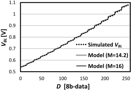
Figure 2.13 shows the result from HSPICE simulations for FR when addition (or subtraction) of 4-bit data D and P are obtained by FR. The linearity is measured by integral
non-linearity (INL), and the dynamic range of ∆VBLB is limited to 0.9 V in order to obtain INL
within 2.5 LSB. The tting parameters for the model of (2.17), c0 =−0.003041, c1 = 0.037, and c2 = −0.000243, result in a modeling error less than 0.3 LSB. Figure 2.14 shows the accuracy of sub-ranged read for D with B = 8 from HSPICE simulation. The INL is less
than 6 LSBs and the modeling errors of (2.21) with M = 16 is smaller than 1.6 LSBs.
-7 -6 -5 -4 -3 -2 -1 0 0 0.2 0.4 0.6 0.8 1 1.2 0 5 10 15 20 25 30 35 IN L (L SB )
∆V
B LB[V]
D
+
P
(LSB)
Simulation Model INL Dynamic Range INL ∆VBLBD
+
P
(4b-data)
Figure 2.13: ∆VBLB from simulations and model (2.17) during FR withB = 4, VP RE = 1
V, and T0 = 300 ps. 0.5 0.6 0.7 0.8 0.9 1 1.1 0 50 100 150 200 250
V
BL[V
]
Model (M=14.2)
Model (M=16)
Simulated
V
BLD
[8b-data]
V
B L[V
]
Figure 2.14: Sub-ranged read with HSPICE simulations and behavioral models with
500 550 600 650 700 750 800 850 900
Case1 Case2 Case3 Case4 Case5 Case6 Case7
V
C[mV
]
Simulation
Model
Figure 2.15: VC from circuit simulations and system simulations with behavioral models
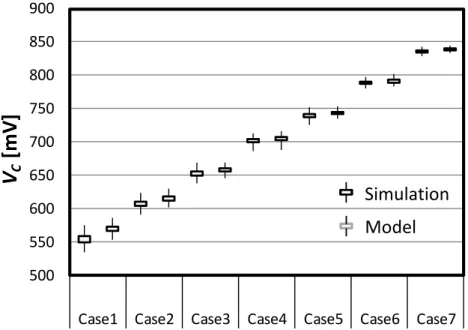
(2.17) to (2.23) when N = 8 and VW L = 800mV.
the bitcell (D) to the nal output (VˆC) with N = 8 are validated in Fig. 2.15. The VC is
achieved from HSPICE Monte-Carlo simulations, and compared with the output obtained from the behavioral models described by (2.17)-(2.23) as shown in Fig. 2.15. Seven dierent combinations of D and P are chosen to measure the accuracy of behavioral models. The
maximum error of the models is 4.4% of the dynamic range of VC and this is suciently
accurate to measure relative magnitude of dierentVCs.
2.5.5.3 Error Behavior
The 4VBL(D)is measured with dierent values of VW L from HSPICE simulations as shown
in Fig. 2.16. The D = 14 = 1110(2) is chosen to maximize σ4VBL(D)/µ4VBL(D) as the BL
is discharged by a single transistor without an averaging-out eect. The σ4VBL(D) is also
measured from Monte-Carlo simulations with HSPICE to estimateσ2
4VBL(D,P)via (2.19) and
(2.20), which are used for the system simulations to estimate the PDET of DIMA. Energy
eciency of DIMA is improved by reducing VW L due to low BL swing whereas the variation
of FR is increased as shown in Fig. 2.16 as the access transistor operates in near-threshold voltage regime.
0 0.05 0.1 0.15 0.2 0.25 0.3 0.35 0 10 20 30 40 50 300 400 500 600 700 800 900 1000
σ
ΔVBL/μ
Δ VBLΔ
V
BL[mV
]
VWL[mV]Figure 2.16: 4VBL(D) and σ4VBL(D)/µ4VBL(D) for D= 14 with N = 4.
0 5 10 15 20 25 30 35 40 1 2 4 8 16 32 64 128 256 512
E[
η
2 C]