An Electrically Small Antenna Using Defected Ground Structure
for RFID, GPS and IEEE 802.11 a/b/g/s Applications
Riki Patel*, Arpan Desai, and Trushit Upadhyaya
Abstract—A compact size (20 × 21 mm2) planar tri-band electrically small antenna is presented
for Wireless ISM, RFID application resonating at 1.57 GHz, 2.47 GHz and 926 MHz. The Proposed structure consists of a dual-slot radiating patch and two split ring structures made using combination of L and U shapes forming a defected ground structure (DGS). Length and width of the planar slot is optimized to get the required frequency bands whereas incorporation of DGS leads to increase in impedance bandwidth. The simulated and measured return losses (S11) of all three frequency bands
are greater than 10 dB. Impedance bandwidths of 20 MHz (913–934 MHz), 90 MHz (1.5–1.59 GHz) and 70 MHz (2.43–2.50 GHz) are achieved for the proposed range. The electrically small antenna radiation pattern is omnidirectional, and gains of 0.32 dBi, 1.2 dBi and 1.5 dBi are achieved which make the antenna suitable for RFID, GPS and WLAN applications.
1. INTRODUCTION
Electrically small antennas (ESAs) are attracting researchers due to their small size, ease of integration on chipset and multiband characteristics [1]. In wireless communication systems, the need for compact size multiband resonating antennas is increasing day to day. Researchers have proposed many electrically small antennas for various applications using different techniques. There are various single band electrically small antennas proposed in the literature. The authors have proposed an electrically small antenna with semi ground plane for biomedical applications working at 2.45 GHz [2]. ESA’ in the form of active antennas using superconductive serial arrays is presented in [3] which is applicable to 200 MHz. An electrically small slotted antenna for MIMO application where the structure uses meander line combination with semi ground plane antenna is illustrated in [4]. Trident shape with a meandered line electrically small antenna is proposed for single band 2.45 GHz application [5]. Electrically small scalable antenna fabricated on a thin circuit board working at 2.4 GHZ frequency is presented in [6]. A compact size antenna using metamaterial based Taconic TLY-5 conducting material having high gain and circular polarization applicable for WiMAX application is proposed in [7]. With increase in complexity of devices, the demand for multiband antennas is very high, and as a result, various types of dual-band and tri-band antennas for various applications have been reported. Planar inverted F shaped dual-band ESA working at 100 MHz and 500 MHz applicable to handheld application is proposed in [8]. A dual-band circularly polarized four short stub loaded microstrip patch antenna useful for wireless applications is proposed in [9] which is not categorized as compact antenna due to its dimensions. Another antenna using carbon composite as conductive adhesive is proposed for UWB applications having dimensions of 41×41 mm2 [10]. There are various techniques to achieve multiband characteristics such as slot/notch loading, lumped element loading, short circuit microstrip antennas, fractals, artificial magnetic conductors, electromagnetic bandgap (EBG) structures, Split Ring Resonators (SRRs)/Complementary SRRs (CRRs), frequency selective surfaces (FSS) and defected
Received 19 February 2018, Accepted 9 April 2018, Scheduled 24 April 2018
* Corresponding author: Riki Patel ([email protected]).
ground structure which are implemented in conventional patch antennas [11]. A miniaturized ultra-wideband slotted antenna with dual band notched characteristics is proposed in [12]. A parasitic electrically small dipole antenna having near-field resonance with wide-band characteristics of 300 MHz achieved by incorporating non-Foster component is proposed in [13]. Fractal slots in the form of Jerusalem crosses (JCs) are incorporated for achieving circular polarization where wide band is achieved by four JC cross formations [14]. Various other techniques for performance improvement have been suggested in the literature by using metastructure, monopole antenna with disk structure, ACs fed structure, 3D space base structure, and superconducting outer ring base structures [15, 16]. One more technique of improving the gain is using cavity-backed antenna with complimentary split ring resonators, which is mainly optimized to work at 2.45 GHz having dimension of 70×70 mm2 [17]. Defected Ground Structure is also used for achieving multiband characteristics where the structure is achieved by etching off any shape in ground plane. Depending on the shape of etching and defect on ground plane, the antenna characteristics vary. The transmission line with DGS gives a higher effective impedance and also introduces high slow wave effect, which provides rejection band in some frequency range. Different shapes such as rectangular, circular, dumbbell, spiral, L-shaped, concentric ring, hairpin, square, hexagon-shaped and many more DGS structures have been proposed in the literature [18, 19]. DGS structure is employed in the CPW feed for enhancing the bandwidth, and the gain of patch antenna is proposed in [20]. A DGS structure to suppress higher order harmonics is employed in a low profile ESA which resonates at 1.81 GHz [21].
In this paper, an electrically small antenna structure having multiband characteristics is proposed by incorporating slots on the top side and two square-shaped DGSs on the ground plane. The proposed multiband antenna resonates at 2.47 GHz, 1.57 GHz and 926 MHz which is suitable for Bluetooth/WLAN, GPS (ISM band) and 926 MHz RFID applications. The dimension of the proposed antenna design is smaller than other electrically small antennas in the literature for the proposed frequency bands.
2. ANTENNA DESIGN GEOMETRY AND METHODOLOGY
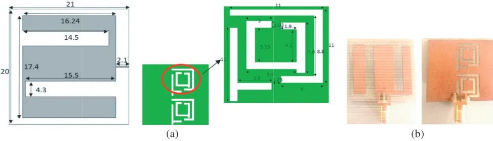
Figures 1(a) and 1(b) show top and bottom sides of the optimized structure of ESA resonating at tri frequency bands. The patch shape is achieved using two slots which are optimized for single band resonance. The bottom plane incorporating defected ground structure (DGS) is formed using square-shaped ring resonators with U and L-square-shaped structures. ESA with DGSs is fed by a high performance 50 Ohm SMA connector. Optimized antenna parameters are as shown in Table 1.
Here FR4 material having dielectric constant of 4.4 and loss tangent of 0.029 is used as the substrate. Overall space occupied by the antenna is 20×21×1.6 mm3. DGSs have low profile, and they are easy to fabricate on FR4 substrates. The U and L shapes forming DGS are optimized after doing parametric study to achieve multiband characteristics of the ESA. In the proposed ESA, higher efficiency is achieved by using dual slots, which leads to capacitance effect giving enhanced current distribution. In small
(a) (b)
Table 1. Antenna parameter (All dimensions are in mm).
Patch DGS side
Patch Llength
×Pwidth 17.4×16.24 inner ring
RLlength
×RWwidth 5.05×1.03 L shaped
LSLlength
×NLlength 11×3.9
Upper slot ULlength
×UWWidth 14.5×4.3 U shaped
USLlength
×Nlength 11×8.8
feeding
strip line FSL 2.1
Lower slot LLlength
×LWWidth 15.5×4.3 Ground W×L 20×21
antennas, the biggest challenge is impedance matching due to small structure of the antenna leading to small radiation flow and large reactance. In our case, the inductive reactance of patch antenna is matched with capacitive loads where small ring oscillator DGS acts as a capacitive load. The gap between the ring, L and U at DGS can provide internal capacitance and inductance at bottom end. Two rings on the ground plane store large electric field, and small gap can provide the capacitance internally. Three frequencies are controlled by changing dimensions of square rings and slot. Accordingly the ESA incorporated with DGS and dual-slot patch antenna is designed working at 926 MHz for RFID, 1.57 GHz for L-band GPS and third band at 2.47 GHz for ISM application.
3. RESULTS AND DISCUSSIONS
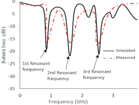
Simulated and measured return loss (S11) results are illustrated in Fig. 2 for tri-band ESA incorporated
with DGS. The return loss of antennas is measured using Agilent Vector Network Analyzer (9914). It is observed that simulated and measured results show great similarity with little variation due to fabrication tolerances. Simulated return loss of compact ESA is 19 dB at 926 MHz, 23 dB at 1.57 GHz and 22.35 dB at 2.47 GHz. The measured impedance bandwidths for S11 <−10 dB are 2.43–2.50 GHz
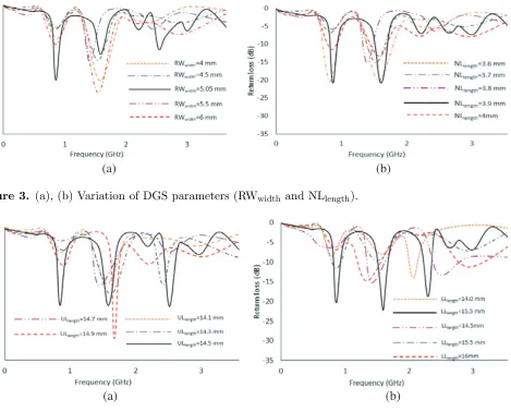
(bandwidth is 20 MHz), 1.5–1.59 GHz (bandwidth is 90 MHz) and 913–934 MHz (bandwidth is 70 MHz) for the proposed tri-band antenna. The measured fractional bandwidth is 5.5% at 926 MHz, 7% at 1.57 GHz and 6% at 2.47 GHz. To achieve required band characteristics, the critical parameters are the dual slots on the patch and its position which are decided after running the parametric variations as shown in Figs. 3 and 4.
Figure 3 shows optimization of RWwidth. When width of the inner ring forming DGS at the ground
plane is varied, frequency at higher side decreases while 1st resonant frequency increases with increase
(a) (b)
Figure 3. (a), (b) Variation of DGS parameters (RWwidth and NLlength).
(a) (b)
Figure 4. Variation of upper slot (a) ULlength and (b) LLlength.
in return loss. Mainly the 2nd frequency has been sifted to higher side and bandwidth increased. Here optimization value of RWwidthis 5.05 mm. Also variation of NLlength leads to change in result where the
3rd resonant frequency has been removed, and the 2nd resonance return loss increases with decrease in the bandwidth. Here optimized value of NLlength is 3.9 mm.
Figure 4(a) shows the optimization of ULlength. When changing the length of lower slot ULlength,
the 2nd frequency range shifts to lower side and 3rd resonance achieved, and the frequency shifts to lower side. The 2nd and 3rd frequency bandwidths change based on Optimization of ULlength. Hence,
optimized ULlength is 14.5 mm. Fig. 4(b) shows the optimization of LLlength. When changing the
ULlength, the 1st resonant range shifts to lower side, and the 2nd resonance shifts to lower side with
changing frequency band bandwidth of antenna. Mainly the 3rd resonance is shifts to higher side ULlength correlated with fringing field effect of antenna. Hence, the optimized ULlength is 15.5 mm.
Current distribution plot is shown in Figure 5 for the targeted frequencies which shows that greater amount of current is distributed at the bottom side of patch at 926 MHz frequency while it is distributed more near the middle part and on the corners in the case of 1.57 GHz frequency. At 2.47 GHz, current distribution is observed near the left part and right center part of the patch.
The ESA is achieved by maintaining the antenna ka = 0.281 for 926 MHz, ka = 0.476 for 1.57 GHz and ka = 0.75 for 2.47 GHz with respect to the bandwidth. The small antenna minimum sphere radius
a = 14.5 mm is calculated using Eq. (1) proposed by Chu [22]. Qchu is 48.79 at 926 MHz, 11.33 at 1.57 GHz, and 3.70 at 2.47 GHz.
(a) (b) (c)
Figure 5. Current Distribution of top view. (a) 926 MHz. (b) 1.57 GHz. (c) 2.47 GHz.
(i) (ii) (iii)
(a)
(b)
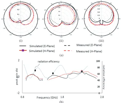
Figure 6. (a) Normalized far-field antenna radiation pattern of (i) 926 MHz, (ii) 1.57 GH and (iii) 2.47 GHz. (b) Simulated (continous line) and Measured (dashed line) Peak gain dBi and black doct as efficiency resonate point.
patch antenna is enclosed in a hypothetical sphere. Based on the quality factor (Q) definition, Chu has defined limitation of a ESAs in the form of Eq. (1) [22, 23].
QChu= 1
ka+
1
k3a3 (1)
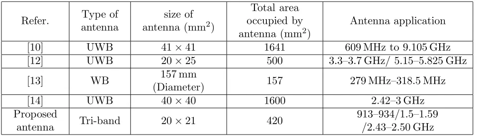
Table 2. Comparison of proposed antenna with other reported multi-band antennas.
Refer. Type of antenna
size of antenna (mm2)
Total area occupied by antenna (mm2)
Antenna application
[10] UWB 41×41 1641 609 MHz to 9.105 GHz [12] UWB 20×25 500 3.3–3.7 GHz/ 5.15–5.825 GHz
[13] WB 157 mm
(Diameter) 157 279 MHz–318.5 MHz
[14] UWB 40×40 1600 2.42–3 GHz
Proposed
antenna Tri-band 20×21 420
913–934/1.5–1.59 /2.43–2.50 GHz
so that a tuning component must be added in series with the antenna to cancel its reactance and assist matching to the circuit to which it is connected. The addition of this extra component creates a tuned circuit, with aQ-factor that potentially limits the instantaneous bandwidth available for signals passing through the antenna. This is a fundamental limit that sets a minimum size for any antenna used at a given frequency and with a given required bandwidth. However, any antenna can be made to show a larger bandwidth than suggested by the Chu limit if there is additional resistance present to reduce the Q, and this has led to claims for antennas that have breached the limit, but none has so far been substantiated. The radiation patterns of the proposed antenna are simulated in theEandHplanes using HFSS and measured in an in-house anechoic chamber using an antenna measurement system for the resonating frequency range of 926 MHz, 1.57 GHz and 2.47 GHz. A standard double-ridged horn antenna is used as the reference antenna. Fig. 6(a) illustrates the simulated and measured normalized far-field antenna radiation patterns. Simulated and measured peak gains at 926 MHz, 1.57 GHz and 2.47 GHz show great correlation where gain values of 0.32 dBi, 1.2 dBi and 1.5 dBi are achieved respectively for the operating band. The simulated antenna radiation efficiencies are 77% at 926 MHz, 46% at 1.57 GHz, and 92% at 2.47 GHz as shown in Fig. 6(b).
The simulated and measured results are found in close agreement with a little difference due to measurement and alignment errors. The radiation patterns deteriorate at higher frequencies as the equivalent radiating area changes with frequency over the operating band.
A comparison table in terms of antenna size, antenna purpose, total area occupied by the antenna and its frequency of operation is given in Table 2 where it can be observed that the proposed ESA is better than the references in terms of size and multiband characteristics.
4. CONCLUSION
A tri-band DGS incorporated electrically small antenna operating at 926 MHz, 1.57 GHz and 2.48 GHz is presented. The measured return loss shows the bandwidth of 1.7% at 926 MHz, 2% at 1.57 GHz and 2% at 2.48 GHz, respectively. Good agreement is observed for simulated and measured results in terms of return loss. The radiation shows omnidirectional pattern for all the three frequencies under consideration. Thus, the antenna is suitable to be used in many applications such as 2.47 GHz Bluetooth/WLAN, 1.57 GHz GPS (ISM band in India) and 926 MHz RFID applications.
REFERENCES
1. Patel, R. H. and T. K. Upadhyaya, “Compact planar dual band antenna for WLAN application,”
Progress In Electromagnetics Research Letters, Vol. 70, 89–97, 2017.
2. Patel, R. and T. Upadhyaya, “An electrically small antenna for nearfield biomedical applications,”
Microwave and Optical Technology Letters, Vol. 60, No. 3, 556–561, 2018.
3. Kornev, V. K., et al., “Active electrically small antenna based on superconducting quantum array,”
4. Bhad, M. C., V. G. Kasabegoudar, and M. P. Rodge, “Electrically small rectangular patch antenna with slot for MIMO applications,” Wireless and Mobile Technologies, Vol. 1, No. 1, 25–28, 2013. 5. Ren, X., X. Chen, and K. Huang, “A novel electrically small meandered line antenna with a
trident-shaped feeding strip for wireless applications,”International Journal of Antennas and Propagation, Vol. 2012, 2012.
6. Sum, Y. L., et al., “Scalable 2.45 GHz electrically small antenna design for metaresonator array,”
The Journal of Engineering, Vol. 1, No. 1, 2017.
7. Kuhestani, H., M. Rahimi, Z. Mansouri, F. B. Zarrabi, and R. Ahmadian, “Design of compact patch antenna based on metamaterial for WiMAX applications with circular polarization,” Microwave and Optical Technology Letters, Vol. 57, No. 2, 357–360, 2015.
8. El Halaoui, M., et al., “Multiband planar inverted-F antenna with independent operating bands control for mobile handset applications,” International Journal of Antennas and Propagation, Vol. 2017, 2017.
9. Heidari, A. A., M. Heyrani, and M. Nakhkash, “A dual-band circularly polarized stub loaded microstrip patch antenna for GPS applications,” Progress in Electromagnetics Research, Vol. 92, 195–208, 2009.
10. Reyes-Vera, E., et al., “Development of an improved response ultra-wideband antenna based on conductive adhesive of carbon composite,”Progress In Electromagnetics Research, Vol. 79, 199–208, 2017.
11. Khanna, R., “A review of various multi-frequency antenna design techniques,” Indian Journal of Science and Technology, Vol. 10, No. 16, 2017.
12. Mahmoud Ali, M. M., A. A. R. Saad, and E. E. M. Khaled, “A design of miniaturized ultra-wideband printed slot antenna with 3.5/5.5 GHz dual band-notched characteristics: Analysis and implementation,”Progress In Electromagnetics Research B, Vol. 52, 37–56, 2013.
13. Zhu, N. and R. W. Ziolkowski, “Broad-bandwidth, electrically small antenna augmented with an internal non-Foster element,” IEEE Antennas and Wireless Propagation Letters, Vol. 11, 1116– 1120, 2012.
14. Heydari, S., P. Jahangiri, A. S. Arezoomand, and F. B. Zarrabi, “Circular polarization fractal slot by Jerusalem cross slot for wireless applications,” Progress In Electromagnetics Research, Vol. 63, 79–84, 2016.
15. Shivapanchakshari, T. G. and H. S. Aravinda, “Review of research techniques to improve system performance of smart antenna,” Open Journal of Antennas and Propagation, Vol. 5, No. 02, 83, 2017.
16. Vera, E. R., F. Lopez, D. E. Senior, and D Cata˜no, “Performance analysis of a microstrip patch antenna loaded with an array of metamaterial resonators,” 2016 IEEE International Symposium on Antennas and Propagation (APSURSI), 281–282, 2016.
17. Memarzadeh-Tehran, H., R. Abhari, and M. Niayesh, “A cavity-backed antenna loaded with complimentary split ring resonators,” AEU-International Journal of Electronics and Communications, Vol. 70, No. 7, 928–935, 2016.
18. Zhang, C., J. Zhang, and L. Li, “Triple band-notched UWB antenna based on SIR-DGS and fork-shaped stubs,”Electronics Letters, Vol. 50, No. 2, 67–69, 2014.
19. He, Z., J. Cai, Z. Shao, X. Li, and Y. Huang, “A novel power divider integrated with SIW and DGS technology,” Progress In Electromagnetics Research, Vol. 139, 289–301, 2013.
20. Singh, A. and S. Singh, “A novel CPW-fed wideband printed monopole antenna with DGS,” AEU-International Journal of Electronics and Communications, Vol. 69, No. 1, 299–306, 2015.
21. Kimouche, H. and S. Oukil, “Electrically small antenna with defected ground structure,” 2012 42nd European Microwave Conference, 811–814, Amsterdam, 2012.
22. Chu, L. J., “Physical limitations on omni-directional antennas,” Journal of Applied Physics, Vol. 19, l163–1175, 1948.
23. Patel, R. H., A. Desai, and T. Upadhyaya, “A discussion on electrically small antenna property,”