Pi Controller Based Soft-Switching Two-Switch Resonant Ac–Dc
Converter with High Power Factor
C.Sukumar & Dr.Chidhambaraiah Setty
#1M.Tech Student, #2professor,
Department of EEE
St.Johns College of Engineering &Technology, Yerrakota,Yemmiganur,Kurnool ,Andhra Pradesh
ABSTRACT: In this project a Soft-switching two-switch resonant power factor correction (PFC) converter is proposed with closed loop PI contoller. In this converter, a boost PFC circuit is combined with a soft-switching resonant converter and PI. Boost converter is used to achieve the power factor correction (PFC). The voltage across the main switches is improved to the dc-link voltage and the energy of the transformer leakage inductance is reused. Soft-switching operation of main switches and output diodes is getting in a resonant manner and output feed given to the pi controller the switching losses are significantly reduced. Therefore, the overall efficiency is improved. A simulation of the 48 V, 60W converter is presented.
I. INTRODUCTION
INRECENT years, industrial demand for high-energy efficiency and low-harmonic-pollution ac–dc converters with active PFC has increased rapidly. These converters are divided into single-stage types and two-stage types according to their structures. For a two-two-stage ac–dc converter, two power processing stages are cascaded [1], [2]. One is a PFC stage, and the other is a DC–DC stage for tightly regulated output voltage. Although the two-stage ac–dc converter achieves good performance (including high power factor and low voltage stress), it has the disadvantages of high component count, large size, high cost, and low power-conversion efficiency. In a singlestage converter, a PFC stage and a DC–DC stage are merged to share common switches so that the total component count is reduced and single power processing is achieved [3]–[18]. Therefore, the demand for a single-stage ac–dc converter has grown significantly because of this converter’s small size, low cost, and high energy efficiency. In this converter, a boost PFC circuit is integrated with a soft-switching resonant converter. High power factor is achieved by the boost PFC circuit. A conventional boost flyback converter. A boost-flyback converter has advantages such as a simple structure and low cost , However, switching losses and electromagnetic interference (EMI) emissions are significant due to hard-switching operation of hard-switching devices. In addition, an
additional snubber circuit is required to suppress the voltage stress across a main switch. Main advantages id No power losses, High efficiency, Low manufacturing costs medium and high power applications
II. FLYBACK CONVERTER:
The flyback converter is based on the buck-boost converter. Its derivation is illustrated in Fig. 1. Figure 1(a) depicts the basic buck-boost converter, with the switch realized using a MOSFET and diode. In Fig. 1(b), the inductor winding is constructed using two wires, with a 1:1 turns ratio. The basic function of the inductor is unchanged, and the parallel windings are equivalent to a single winding constructed of larger wire. In Fig. 1(c), the connections between the two windings are broken. One winding is used while the transistor Q1 conducts, while the other winding is used when diode D1 conducts. The total current in the two windings is unchanged.
The behavior of most transformer-isolated converters can be adequately understood by modeling the physical transformer with a simple equivalent circuit consisting of an ideal transformer in parallel with the magnetizing inductance. The magnetizing inductance must then follow all of the usual rules for inductors; in particular, volt-second balance must hold when the circuit operates in steady-state. This implies that the average voltage applied across every winding of the transformer must be zero.
Let us replace the transformer of Fig. 1(d) with the equivalent circuit described above. The circuit of Fig. 2(a) is then obtained. The magnetizing inductance LM functions in the same manner as inductor L of the original buck-boost converter of Fig. 1(a). When transistor Q1 conducts, energy from the dc source Vg is stored in LM. When diode D1 conducts, this stored energy is transferred to the load, with the inductor voltage and current scaled according to the 1:n turns ratio.
dominant for stability during operation). Both require a signal related to the output voltage. There are three common ways to generate this voltage. The first is to use an optocoupler on the secondary circuitry to send a signal to the controller. The second is to wind a separate winding on the coil and rely on the cross regulation of the design. The third consists on sampling the voltage amplitude on the primary side, during the discharge, referenced to the standing primary DC voltage.
III.RESONANT CONVERTER
Resonant inverters are electrical inverters based on resonant current oscillation. In series resonant
inverters the resonating components
and switching device are placed in series with the load to form an under damped circuit. The current through the switching devices fall to zero due to the natural characteristics of the circuit. If the switching element is a thyristor, it is said to be self-commutated.
IV.SOFT SWITCHING
Semiconductors utilised in Static Power Converters operate in the switching mode to maximise efficiency. Switching frequencies vary from 50 Hz in a SCR based AC-DC Phase Angle Controller to over 1.0 MHz in a MOSFET based power supply. The switching or dynamic behaviour of Power Semiconductor devices thus attracts attention specially for the faster ones for a number of reasons: optimum drive, power dissipation, EMI/RFI issues and switching-aidnetworks. With SCRs’ 'forced commutation' and 'natural (line) commutation' usually described the type of switching. Both refer to the turn-off mechanism of the SCR, the turn-on dynamics being inconsequential for most purposes. A protective inductive snubber to limit the turn-on di/dt is usually utilised. For the SCRs’ the turn-off data helps to dimension the 'commutation components' or to set the 'margin angle'. Conduction losses account for the most significant part of total losses. Present day fast converters operate at much higher switching frequencies chiefly to reduce weight and size of the filter components. As a consequence, switching losses now tend to predominate, causing the junction temperatures to rise. Special techniques are employed to obtain clean turn-on and turn-off of the devices. This, along with optimal control strategies and improved evacuation of the heat generated, permit utilisation of the devices with a minimum of deration. This chapter first examines the switching process, estimates the device dissipation and indicates design procedures for the cooling system Losses in Power Semiconductors
A converter consists of a few controlled and a few uncontrolled devices (diodes). While the first device is driven to turn-on or off, the uncontrolled device operates
mainly as a slave to the former. Power loss in the converter is the aggregate of these losses. Occasionally the diode and the controlled device are housed in the same module. The losses corresponding to each contribute to the temperature rise of the integrated module.
Switching Losses
IGBTs are designed for use in switching converters and not for linear operation. This means switching time intervals are short compared to the pulse duration at typical switching frequencies, as can be seen from their switching times, such as rise time tr and fall time tf in the data sheets. Switching losses occur during these switching intervals
ZERO VOLTAGE SWITCHING
The switches of a ZVS resonant converter turn on and turn off at zero voltage. A zero-voltage switching technique is described that utilizes a resonant transition during a short but finite switching interval. This zero-voltage resonant-transition (ZVRT) switching technique can be applied to conventional buck, boost, and buck-boost power converter topologies that operate with a constant switching frequency and use pulse width modulation for output control. Since frequency-dependent losses are greatly reduced in the power transistors, efficient operation at higher switching frequencies (>1 MHz) is allowed. However, conduction losses are increased because ripple currents are increased and synchronous rectification is required.
THD:
Total harmonic distortion (THD) is a complex and often confusing concept to grasp. However, when broken down into the basic definitions of harmonics and distortion, it becomes much easier to understand. Now imagine that this load is going to take on one of two basic types: linear or nonlinear.
waveform distortions are created. Thus waveform distortions can drastically alter the shape of the sinusoid.
However, no matter the level of complexity of the fundamental wave, it is actually just a composite of multiple waveforms called harmonics.
Fig.A. Ideal sine wave Fig.B. Distorted waveform
Harmonics have frequencies that are integer multiples of the waveform’s fundamental frequency. For example, given a 60Hz fundamental waveform, the 2nd, 3rd,4th and 5th harmonic components will be at 120Hz, 180Hz,
240Hz and 300Hz respectively. Thus, harmonic distortion is the degree to which a waveform deviates from its pure sinusoidal values as a result of the summation of all these harmonic elements. The ideal sine wave has zero harmonic components. In that case, there is nothing to distort this perfect wave.
Total harmonic distortion, or THD, is the summation of all harmonic components of the voltage or current waveform compared against the fundamental component of the voltage or current wave:
POWER FACTOR
The power factor of an AC electrical power system is defined as the ratio of the real power flowing to the load,
to the apparent power in the circuit, and is a dimensionless number between -1 and 1. Real power is the capacity of the circuit for performing work in a particular time. Apparent power is the product of the current and voltage of the circuit. Due to energy stored in the load and returned to the source, or due to a non-linear load that distorts the wave shape of the current drawn from the source, the apparent power will be greater than the real power. A negative power factor occurs when the device which is normally the load generates power which then flows back towards the device which is normally considered the generator. In an electric power system, a load with a low power factor draws more current than a load with a high power factor for the same amount of useful power transferred. The higher currents increase the energy lost in the distribution system, and require larger wires and other equipment. Because of the costs of larger equipment and wasted energy, electrical utilities will usually charge a higher cost to industrial or commercial customers where there is a low power factor.Linear loads with low power factor (such as induction motors) can be corrected with a passive network of capacitors or inductors. Non-linear loads, such as rectifiers, distort the current drawn from the system. In such cases, active or passive power factor correction may be used to counteract the distortion and raise the power factor. The devices for correction of the power factor may be at a central substation, spread out over a distribution system, or built into power-consuming equipment.
BUCK CONVERTER
The basic operation of the buck converter has the current in an inductor controlled by two switches (usually a transistor and a diode). In the idealised converter, all the components are considered to be perfect. Specifically, the switch and the diode have zero voltage drop when on and zero current flow when off and the inductor has zero series resistance. Further, it is assumed that the input and output voltages do not change over the course of a cycle (this would imply the output capacitance as being infinite).
Buck converter is also called as step down chopper it means the average output voltage is less than the input voltage.
two semiconductors (a diode and a transistor) and at least one energy storage element, a capacitor, inductor, or the two in combination. Filters made of capacitors (sometimes in combination with inductors) are normally added to the output of the converter to reduce output voltage ripple
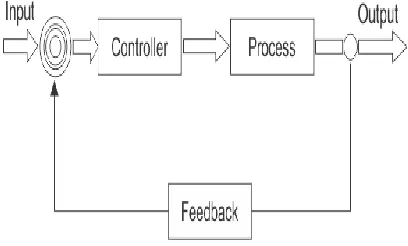
Closed Loop Control System
Control system in which the output has an effect on the input quantity in such a manner that the input quantity will adjust itself based on the output generated is called closed loop control system. Open loop control system can be converted in to closed loop control system by providing a feedback. This feedback automatically makes the suitable changes in the output due to external disturbance. In this way closed loop control system is called automatic control system. Figure below shows the block diagram of closed loop control system in which feedback is taken from output and fed in to input.
Fig 4.2 Block diagram of open loop system Proportional and Integral Controller
As the name suggests it is a combination of proportional and an integral controller the output (also called the actuating signal) is equal to the summation of proportional and integral of the error signal. Now let us analyze proportional and integral controller mathematically. As we know in a proportional and integral controller output is directly proportional to the summation of proportional of error and integration of the error signal, writing this mathematically we have,
R emoving the sign of proportionality we
have, W
here, Ki and kp proportional constant and integral
constant respectively.
Advantages and disadvantages are the combinations of the advantages and disadvantages of proportional and integral controllers.
Fig 4.3 PI controller
V. PROJECT DESCRIPTION
results for a 60-W prototype of the proposed converter are presented to verify the performance of the proposed converter
Operation of Proposed Converter
The equivalent circuit of the proposed converter is shown in Fig. 3. For simplicity in the input stage, the EMI input filter Lf and Cf and a bridge diode are disregarded. The input voltage is expressed as the rectified line voltage |vin|. The boost PFC cell is composed of a boost inductor Lb, reverse-blocking diode Db, and a main switch S1. In the two-switch resonant DC– DC module, the transformer T1 is modeled as the magnetizing inductance Lm, the leakage inductance Lk, and an ideal transformer with a turn ratio of n:1. To simplify the mathematical analysis of the resonance between Lk and C1, the total transformer leakage inductance Lk is referred to the secondary side. The capacitor Cdc is a DC-bus capacitor. The snubber diodes D1 and D2 are cross-connected across the main switches S1 S2, and the primary winding. The diodes DS1 and DS2 are the intrinsic body diodes of main switches S1 and S2. Capacitors CS1 and CS2 are the parasitic output capacitances of their respective switches. Key waveforms of the proposed converter are shown in Fig. 4. The main switches S1 and S2 are turned ON or OFF at the same time by a gate driver. The switching period Ts is given by 1/fs, where fs is the switching frequency.
Mode 1 [t0, t1]:
At t0, when voltage vs1 is a minimum value, both switches S1 and S2 are turned ON at the same time. This is called near zero-voltage switching (ZVS), and it minimizes the power dissipation at turn-ON. Since the boost inductor voltage vLb is Vin, the boost inductor current iLb increases linearly. In the secondary of T1, with the turn-ON of S1 and S2, output diode Do2 starts to conduct, and resonance occurs between the leakage inductance Lk and the capacitor C1. Output diode Do1 is reverse-biased as Vo.
Mode 2 [t1, t2]:
At t1, when the leakage inductance current iLk reaches zero by resonance between Lk and C1, this mode begins. Zero-current turn-OFF of diode Do2 is achieved. The inductance current iLm increases linearly from I1 with a slope of Vdc/Lm. At the end of this mode, the inductor currents iLm arrive at their maximum value I1. The current I1 can be In the secondary of the transformer T1, the leakage inductance current iLk is zero. Hence, output diodes Do1 and Do2 are turned OFF. Output diode Do1 is reverse-biased as Vo − VDo2 and output diode Do2 is
reverse-biased as Vo − VDo1. In this mode, the output diode voltages vDo1 and vDo2
Mode 3 [t2, t3]:
At t2, both switches S1 and S2 are turned OFF at the same time. Since there is leakage inductance at the primary of the transformer T1, snubber diodes D1 and D2 are turned ON by the current in the leakage inductance. Hence, the voltage vLm across the inductor Lm is -Vdc. The inductor current iLm decreases linearly from I1 with a slope of -Vdc/Lm.
Mode 4 [t3, t4]:
At t3, when the snubber diode current iD1 reaches zero, this mode begins. However, snubber diode D2 is not turned OFF by the reverse-blocking diode Db. Therefore, main switch voltages vs1 and vs2 are vdc and vdc − vLm − vS1. t the end of this mode, boost inductor current iLb arrives at zero. The voltage vLm across inductor Lm is reflected the voltage of the secondary of the transformer T1
Mode 5 [t4, t5]:
At t4, when the boost inductor currents reach zero, this mode begins. Snubber diodes D1 and D2 are turned OFF. Main switch voltage vS1 and snubber diode voltage vD1
VII. CONCLUSION:
In this paper, a soft-switching two-switch resonant ac–dc converter with high power factor is presented. In the proposed converter, since the boost PFC circuit operates in DCM, a high power factor is achieved and control circuit is simple. Voltage stress of main switches and
diodes is reduced by utilizing two-switch structure and the voltage doubler of output stage. Moreover, the absorbed energy from the leakage inductors is reprocessed by the DC–DC module. Due to CRM operations of DC–DC module, switching losses of main switches are significantly reduced. Also, ZCS operation of output diodes is achieved by resonance manner. Therefore, the proposed converter alleviates the reverse-recovery losses of the output diodes. Hence, the proposed converter provides high efficiency. The experimental results, based on a prototype, are presented for validation.
REFERENCES
[1] S.-Y. Cho, I.-O. Lee, J.-E. Park, and G.-W. Moon, “Two-stage configuration for 60W universal-line AC-DC adapter,” in Proc. 38th Annu. IEEE Ind. Electron. Soc. Meet. (IECON’12), 2012, pp. 1445–1450.
[2] J.-E. Park, J.-W. Kim, B.-H. Lee, and G.-W. Moon, “Design on topologies for high efficiency two-stage AC-DC converter,” in Proc. 7th Int. Power Electron. Motion Control Conf. (IPEMC’12), 2012, pp. 257–262.
[3] S.-Y. Ou and H.-P. Hsiao, “Analysis and design of a novel single-stage switching power supply with half-bridge topology,” IEEE Trans. Power Electron., vol. 26, no. 11, pp. 3230–3241, Nov. 2011.
[4] M. K. Kazimierczuk andW. Szaraniec, “Electronic ballast for fluorescent lamps,” IEEE Trans. Power Electron., vol. 8, no. 4, pp. 386–395, Oct. 1993.
[5] K. Jirasereeamornkul, M. K. Kazimierczuk, I. Boonyaroonate, and K. Chamnongthai, “Single-stage electronic ballast with class E rectifier as power-factor corrector,” IEEE Trans. Circuits Syst. I, Reg. Papers, vol. 53, no. 1, pp. 139–148, Jan. 2006.