Design and Analysis of Rectangular
Conducting Slots Based Substrate Integrated
Waveguide
Karan Mahajan
1, Sourabh Mahajan
2PG Student, Dept. of ECE, Sri Sai College of Engineering & Technology, Badhani Pathankot, India1
Assistant Professor, Dept. of ECE, Sri Sai College of Engineering & Technology, Badhani Pathankot, India2
ABSTRACT: The demand for high performance, high gain, low cost, easy to fabricate and compact antennas for telecommunication and different applications has rapidly increased at microwave and higher frequencies. Substrate Integrated Waveguides (SIW) is planar in nature so it can be fabricated on planar circuits like Printed Circuit Boards (PCB) and can be integrated with other planar transmission lines like microstrips.Substrate Integrated Waveguides (SIW) keep the low loss property of their conventional metallic waveguides and are extensively used as interconnection in high speed circuits, filters, directional couplers, antennas. In this paper a Substrate Integrated Waveguide based antenna using rectangular slots is proposed and its integration with Microstrip line. ComsolMultiphysics is used for simulation results.
KEYWORDS: Substrate integrated waveguide, dielectric filled waveguide, electric field, rectangular slots, microwave systems.
I.INTRODUCTION
During recent times, the development of microwave communication systems is growing rapidly. Day by day increase in the demand of hand held communication sets and internet technology put an emphasis on new communication systems with high sensitivity and selectivity, light weight, compact size and low insertion loss [1]. In high frequency applications, micro-strip devices are not efficient, and because wavelength at high frequencies are small, micro-strip device manufacturing requires very tight tolerances. At high frequencies waveguide devices are preferred; however their manufacturing process is difficult. Therefore a new concept emerged; substrate integrated waveguide (SIW). SIW is a transition between micro-strip and dielectric-filled waveguide (DFW). Waveguides shows excellent performance but are expensive and difficult to synthesize due to high volume and bulkiness. Moreover, their integration with other planar circuits is complex [2]. Substrate integrated waveguide (SIW) has been proposed as a new planar structure which are suitable to integrate with the planar structures. Recently, the SIW systems has been explored and implemented by several researchers for number of applications such as radiated RF/microwave components, transmission lines, filters, couplers, diplexers, oscillators, and leaky-wave antennas. These systems gave rise to new and novel small scale waveguides [3-5]. In a SIW structure, the electric field distribution fill the volume inside the waveguide and surface current propagate on a large cross-sectional area of the waveguide walls, resulting in low conducting and insertion losses [6]. Substrate integrated waveguide (SIW) is also believed to be the potential candidate for developing millimeter wave devices [7]. Due to continuous increase in the frequency of operation and circuit density, the closely spaced micro-strip and strip line interconnects and systems will no longer be feasible [8].
In this work, a SIW with rectangular vias and slots have been designed and analyzed mathematically to investigate their different output factors. The design is simulated using FEM based ComsolMultiphysics software after theoretical analysis. A brief introduction about the substrate integrated waveguide is discussed in the next section, while the methodology and the results are explained in subsequent sections followed by logical conclusion.
II. SUBSTRATE INTEGRATED WAVEGUIDE
filled waveguide (DFW), therefore the starting point can be DFW. A schematic for the rectangular waveguide is shown in Fig. 1. For TE10 mode, the dimension b is not important as it does not affect the cut-off frequency of the waveguide [9]. Therefore, the substrate can be of any thickness but it can affect the dielectric losses. More is the thickness, lower are the dielectric losses.
Fig.1. (a) 3D schematic of rectangular waveguide, (b) Top view of 2D equivalent diagram
For a rectangular waveguide, cut off frequency of arbitrary mode is found by the following formula
2 2
2
cc
m
n
f
a
b
(1)wherec is the speed of light in vacuum, m and n are the mode numbers, and a, b are the dimensions of the waveguide. For TE10 mode, the above formula can be simplified as
2
cc
f
a
(2) For DFW with same cut off frequency, the dimension ad is found asd R
a
a
(3) After calculating the dimension a for DFW, the design equations for SIW can be calculated as2
0.95
s dd
a
a
p
(4) where, d is the diameter of the via, and p is the pitch (distance between the vias).For SIW design, the following two conditions are required
5
g
d
(5)
and,
p
2
d
(6)where
g (guided wavelength) can be written as2 2 2
2
(2
)
g Rf
c
a
of a related rectangular waveguide with an equivalent width [10]. We assume that the width between the two rows of metallic cylinders of the SIW is W, the diameter of metalized via hole is D, and the space between adjacent via hole is S. The equivalent width of the SIW is written as follows
2 2
1.08
0.1
effD
D
W
W
S
W
Therefore, the propagation constant of the SIW can written as
2 2
(
)
eff
W
W
The propagation constant 𝛽 is determined by the width W of SIW completely for given D, S, 𝜔,
, and
.
SIW structure has high Q-factor and high power-handling capability with self consistent electrical shielding which are the merits of these structures over conventional metallic waveguide [11].III. PROPOSED DESIGN
The structure of the proposed designed for SIW is shown in Fig. 2. The whole microwave system has been integrated on the same substrate without any mechanical features. A 50 Ω transmission line as characteristic impedance is connected to integrated waveguide. Mode matching is done by tapered section to transform the quasi-TEM mode of the micro-strip line into the TE10 mode. The model of the proposed designed has been optimized in a software for the desired frequency bandwidth, that is, between 6 GHz to 11 GHz. The typical part of modeling is to adjust and optimize the metallic rectangular via holes. The whole structure has been designed according to the analytical equation. This designed structure consists of SIW with the top and bottom metal planes of a substrate having two parallel rectangular via fences in the substrate.
Fig.2. 3D schematic of the proposed design.
For this design, TE10 mode is supported due to their similar current distributions on the side walls. In our design, PCB has been taken as substrate with relative permittivity 3.38 and relative permeability 1. The model is designed using electromagnetic, frequency domain solver. The selected bandwidth of a desired frequency band is applied through the
Table 1: Dimensional parameters selected for SIW design
Parameter Value
Substrate thickness 15 mm
Substrate length 35 mm
Substrate width 12.5 mm
Feed line length 30 mm
Feed line width 3.2 mm
Radius of via 0.5 mm
IV. RESULTS AND DISCUSSIONS
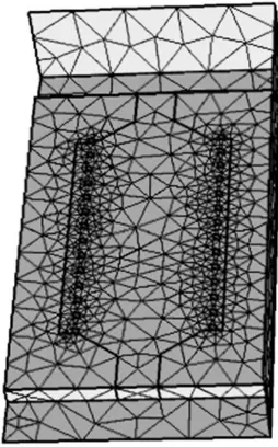
Fig. 3 shows the meshed design of the proposed model. Normal meshing is done on the SIW structure. For this, the maximum element size selected is 0.0054508. The design was simulated on the computational machine with 3.1 GHz processor speed. The virtual memory used while simulation was 2.7 GB. Higher meshing is not selected as the computational load increases for higher mesh sizes.
Fig.3. Meshed design of the proposed model.
Fig.4. Electric field generated in proposed SIW
The results were evaluated by the plot as shown in figure 5. This graph indicates relation observed between S-parameters and the frequency. Return losses or input reflection coefficient (S11) and the forward transmission gain (S21) were plotted. The graph showed that the dip for return loss is observed at 7 GHz frequency and transmission gain remains varied for the whole frequency band but shows maxima at the resonant frequency (7 GHz).
Fig.5. Plot between S-parameters and frequency
From the plot, it is observed that the useful bandwidth (below -10 dB) for the design is in-between 6.8 GHz to 7.4 GHz. Hence the operating bandwidth for this simulated design is approximately 600 MHz.
V.CONCLUSION
REFERENCES
[1] B. N. Das, K. V. S. V. R. Prasad, and K. V. S. Rao (1996), Excitation of Waveguide by Stripline and Microstrip-Line-Fed Slots, IEEE Transactions on Microwave Theory and Techniques, vol. 34, pp. 321327.
[2] C. Xiao-Ping and W. Ke (2008), Accurate and efficient design approach of substrate integrated waveguide filter using numerical TRL calibration technique, in Microwave Symposium Digest, 2008 IEEE MTT-S International, pp. 1231-1234. D
[3] D. Deslandes and K. Wu, “Accurate modeling, wave mechanisms, and design considerations of a substrate integrated waveguide,” IEEE Trans. Microw. Theory Tech., vol. 54, no. 6, pp. 2516–2526, 2006
[4] M. Bozzi, A. Georgiadis and K. Wu, “Review of substrate-integrated waveguide circuits and antennas,” IET Microw. Antennas Propag., vol. 5, no. 8, pp. 909–920, 2008.
[5] Yasser Arfat, Sharad P. Singh, SandeepArya, Saleem Khan, "Modelling, Design and Parametric Considerations for different Dielectric Materials on Substrate Integrated Waveguide," WSEAS Transactions on Communications, Vol. 13, pp. 94-98, 2014.
[6] T. Y. Huang, T. M. Shen and R. B. Wu. Design and Modeling of Microstrip Line to Substrate Integrated Waveguide Transitions, Passive Microwave Components and Antennas, Chapter 11, pp. 225247, InTech, ISBN 978-953-307-083-4.
[7] L. Yan, W. Hong, K. Wu, and T. J. Cui (2005), Investigations on the propagation characteristics of the substrate integrated waveguide based on the method of lines, Microwaves, Antennas and Propagation, IEE Proceedings -, vol. 152, pp. 35-42.
[8] Yasser Arfat, Sharad P. Singh, Saleem Khan and SandeepArya, "Modelling and Design of Substrate Integrated Waveguide using Two Parallel Rows of Rectangular Conducting Slots," International Journal of Current Engineering and Technology, Vol.3, No.5, pp. 2101-2103, 2013. [9] K. Wu, D. Deslandes and Y. Cassivi, "The Substrate Integrated Circuits - A New Concept for High-Frequency Electronics and
Optoelectronics," TELSKIS 2003, Nis, Serbia and Montenegro, pp. Oct. 2003