Implementation on STM-16 Frame Termination
VLSI with High-Speed and Low-Power GDI
Techniques
G.Gowri Lakshmi
1, V.Abila
2, K.Birndhadevi
3PG Student [VLSI], Dept. of ECE, Vivekanandha College of Engg for Women, Tiruchengode, Tamilnadu, India
PG Student [VLSI], Dept. of ECE, Vivekanandha College of Engg for Women, Tiruchengode, Tamilnadu, India
Assistant professor, Dept. of ECE, Vivekanandha College of Engg for Women, Tiruchengode, Tamilnadu, India
ABSTRACT: Many of the current wireline networks are digitalized, In Japan, a synchronous digital hierarchy (SDH) system is installed in the public switched telephone network, and appliance data are transferred with a synchronous transfer module (STM). In this system to put together the advanced STM-16 using the CMOS technology in the technique. The STMs are constructed hierarchically with a nested structure. When commerce with the data for high-speed digital services, a nested level of four is required for each STM; that is, the lowest level of container, virtual container, administrative unit (AU), AU group, and STM. The VLSI has two kinds of I/O ports; one serial port operating at 2.5 Gb/s/pin and sixteen 8-b parallel ports operating at 19.5 Mb/s/pin. The high-speed port is connected to the set of connections side, while the low-speed ports are connected to the fatal sides including tool switches.Using CMOS technique with STM-16 frame termination VLSI, the power utilization during the sampled by is 34 mW, and that for 2.5Gb/s operation is 1.2w at 25 °C.the proposed Gate Diffusion Technique(GDI) allows reducing power consumption, delay and area of digital circuits, while maintaining low difficulty of logic design.A multiplicity of logic gates have been implemented in 0.35 μm technology to compare the GDI technique with CMOS and PTL. A prototype test chip of STM-16 has been fabricated, based on GDI and CMOS cell libraries, showing up to 45% reduction in power-delay product in GDI.
KEYWORDS: STM-16, CMOS, high speed, low power, GDI technique, PTL, frame termination, SDH.
I.INTRODUCTION
INNOVATIONS in device technology including very large-scale integrated circuits (VLSIs), semiconductor lasers, Photodiodes, and optical fibers are having a great brunt on telecommunications. Many wire line networks are digitalized, and “toll switches” are connected to one another with optical fiber cables, which are mainly used to broadcast highly multiplexed digital data. In the fixed-line phone system, sending person’s voice is sampled every 125 μs and converted to 8-b digital data by the sender’s-side “local switch.” Using a public switched telephone network, the data are agreed to the receiver’s-side local switch and reconverted to the original voice.
The SDH defines dedicated transmission frames, called“synchronous transfer modules” (STMs) for every individual multiplex level, where a frame is a transmission data package. Five kinds of frames have been defined: STM-0 (level 0; 52 Mb/s), STM-1 (level 1; 156 Mb/s), STM-4(level 4; 624 Mb/s), STM-16 (level 16; 2.5 Gb/s), and STM-64 (level 64; 10 Gb/s). Every frame at each level has the same configuration in relation to two-dimensional byte data. With STM-1, the frame consists of a 9-row × 9-column“section overhead” and a 9-row × 261-column “payload.”The overhead area, which is 3.3% of the total frame data, is used to store the control data for frame synchronization and/or error checks. Moreover, a part of the overhead area is used to store the data that point the beginning of virtual containers in the payload. The frame frequency at each multiplex level is8 kHz, and the frame data are transmitted bit by bit with an optical fiber cable.
Major requirements for SDH transmission equipment are downsize and power consumption reduction.To reduce power consumption at the required operating speeds, employ a multi-VDD architecture using 2- and1-V power supplies. Also, the use of fully depleted silicon on insulator (FD-SOI) devices is considered from the view point of enhancing the operating speeds and/or reducing the dynamic power dissipation.
The 2-Vmultiplexer/demultiplexer (MUX/DEMUX) macros provide a high operating speed of 2.5 Gb/s, while the dual-port static random access memory (SRAM) macro operates at a low supply voltage of 1 V. Moreover, 50-_-terminated input/output buffers (hereafter termed an I/O buffer) are designed to operate without devoted power supplies, and then a new “direct-drive amplifier” using a feedback reference scheme is devised for a 2-V 2.5-Gb/s input buffer use.
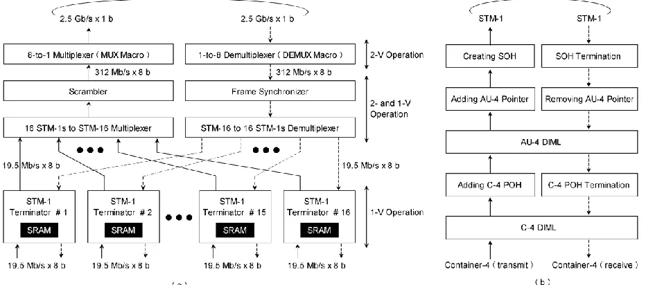
. Fig. 1. STM-16 frame termination VLSI. (a) Configuration. (b) Series of procedures in STM-1 terminator blocks.
II. STM-16 FRAME TERMINATION VLSI
A. DESIGN CONCEPT
The arrangement of our STM-16 frame termination VLSI is shown in Fig. 1(a). The VLSI has two kinds of I/O ports; one serial port operating at 2.5 Gb/s/pin and sixteen 8-bparallel ports operating at 19.5 Mb/s/pin. The high-speed port is connected to the network side, while the low-speed ports are connected to the terminal sides including tool switches. The configurations of STM-16 are defined with STM-1, and so adopt a line of attack that creates sixteen STM-1s as an transitional data form.
The series of procedures required for each STM-1 frame termination is shown in Fig. 1(b). Here, the network side (that is, the core side of the VLSI chip) deals with STM-1 (19.5 Mb/s × 8 b), while the terminal side deals with acontainer-4 (C-4). When packing a C-4 in an STM-1, a “path overhead” and a section overhead consisting of a pointer and control data are attached at a proper nested level. The path overhead consists of the data for monitoring and/or error container and it is stored in the extended area in each payload. When unpacking a received STM-1, the section overhead, the pointer and the path in the clouds are removed at a proper nested level.
In addition, multiplexing to STM-n (n: integer) is performed in the same way. Therefore, adopt a reconfigurable architecture to change the multiplicity with an outside selected mode signal. Our VLSI chip can handle five kinds of STMs: STM-1, −2, −4, −8, and −16, where STM-2 and−8 are prepared only for the VLSI chip test. This function is implemented by 2-V 20-kilogate logic.
B. STRATEGY FOR REDUCING POWER CONSUMPTION
The simplest and most extensively used low power technique is power gating .Cutting off the power supplies for stand by blocks reduces the wasted power dissipation caused by sub threshold leakage currents. The same concept was reported in1996, when “multi threshold voltage CMOS” (MTCMOS) was proposed for mobile applications. The other techniques for reducing active power are clock-signal gating, multiple supply voltages, and “dynamic voltage and frequency scaling” (DVFS). These techniques were developed for specific applications, and so it is important to employ proper low-power techniques to obtain a greater reduction of influence consumption. In CMOS digital VLSIs, a large part of the power consumption is engaged by dynamic components caused by the charge and/or discharge currents for parasitic capacitance. The dynamic power dissipation P is given by (1)
P = C · V2 · f --- (1)
Where C, V, and f are the parasitic capacitance, supply voltage, and operating frequency, respectively. The most effective way to reduce the power dissipation is to lower the supply voltage, but at the same time, the operating speed decreases. Hence, this methodology finds limited use. Another effective way is to reduce the parasitic capacitance. This is also effective in improving the degraded operating speed for low voltage operation.
Multi-VDD Architecture: A feature of the STM-16 frame termination VLSI is that a high operating speed of 2.5 Gb/sis required only for the serial port that includes the peripheral logic. The required operating speed falls to 19.5 Mb/s as it approaches the parallel ports. To consider this situation, use two different kinds of power supplies VDD (typical2 V) and VLL (typical 1 V). With regards to I/O buffers, restrict the use of extra power supplies for terminators and/or references. From the view point of reducing power dissipation, use a 1-V power supply for many components, and the use of a 2-V power supply is restricted to the critical components for which a high operating speed is actually needed. That is, 2.5-Gb/s I/O buffers, a parallel-to-serial converter for byte multiplexing (hereafter termed a MUX macro), a serial-to-parallel converter for byte demultiplexing (i.e., a DEMUX macro) use a 2-V power supply, whereas19.5-Mb/s I/O buffers and STM-1 terminators including dual-port SRAM macros use a 1-V power supply [Fig. 1(a)].Regarding the intermediate blocks operating at 312.5 MHz(i.e., STM-1 to STM-16 MUX, scrambler, synchronizer and STM-16 to STM-1 DEMUX), use a multi-VDD architecture to reduce power consumption without degrading data throughput.
FD-SOI Devices: SOI devices (MOSFETs) have a feature, whereby the parasitic capacitance in the source and/or drain is small because the p-n junction area is greatly reduced compared with bulk devices. Moreover, CMOS/SOI is latch up free. Owing to this feature, the shortened isolation distance between MOSFETs reduces the chip size, resulting in a higher operating speed and/or less dynamic power dissipation.
C. KEY COMPONENT DESIGN
When customizing a standard cell library, a total of two kinds of power lines (VDD and VLL) are installed in every standard cell To suppress the increase in VLSI design cost, the use of macros is restricted to solely the 2-V2.5-Gb/s MUX/DEMUX and 1-V dual-port SRAM. Also, the configuration of 50-Ωterminated I/O buffers is carefully considered to avoid the need for dedicated power supplies.
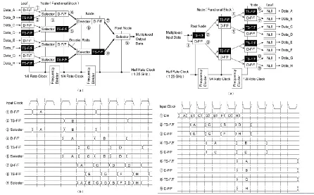
2.5-Gb/s MUX/DEMUX Macros: To achieve the required high operating speed, adopt“complete binary tree” architecture. A functional block and the interconnection between functional blocks are assigned to a “node” and a “path” in the binary tree, respectively. With an8-to-1 MUX, the depth required for the binary tree is three. The functional block for the MUX macro consists of a 2-to-1selector and a cascaded delay flip-flop, whereas that for the DEMUX macro consists of two parallel-connected delay flip-flops. In the architecture, the higher operating frequency limit is provided by the MUX macro not by the DEMUX macro because the MUX macro has 2-to-1 selectors in the critical paths. To enhance the maximum operating incidence of delay flops, consider the use of the double-rail type. The configuration for two-stage delay flip-flops is shown in, compared with that for the conventional single-rail type. A feature of the double-rail type is that it has a pair of complementary inputs and a pair of harmonizing outputs.
.
8-to-1 MUX:The configuration with the complete binary-tree architecture is shown in Fig. 9(a), where D-F/F and TS-F/F are two-stage and three-stage delay flip-flop, respectively. A 1.25-GHz (= f /2) half-rate clock signal with a 50%-duty cycle is provided, while sub rate clock signals at frequencies of 624 MHz (= f/4) and 312 MHz (= f /8) are generated with frequency dividers. Each functional block consists of a 2-to-1 selector and a D-F/F, or a TS-F/F, and it operates synchronously with a half-rate or sub rate clock signal. That is, the data given by a pre stage D-F/F and TS-F/Fare selected in the order of the D-F/F data followed by the TS-F/F data. The data hold time required for the latter multiplexed data are yielded using the TS-F/F instead of a D-F/F. In this way, multiplexed data (i.e., 2-b serial data) are obtained at the output of the functional block.To guarantee the required operating speed of 2.5 Gb/s, eliminate the delay flip-flop from the functional block located at the “root node” and also apply the double-rail type for every functional block located with a depth of one. The single-to-double transfer in the rail configuration is performed on the inside of the flip-flop in each functional block located with a depth of two. That is, the slave latch in a flip-flop is replaced with a double-rail type. Hence, the timing slant between the complementary signals on a pair of wirings is minimized.
1-to-8 DEMUX: The configuration with the complete binary-tree architecture,. In contrast with the MUX, the input is 8-b serial data, while the output is8-b parallel data. That is, the input data pass through the binary tree from the root node to the “leaves.” A 1.25-GHzhalf-rate clock signal with a 50%-duty cycle is provided, while the sub-rate clock signals at frequencies of 624 and312 MHz are generated with frequency dividers. Each functional block consists of a TS-F/F and a D-F/F, and these components operate synchronously with the same frequency clock signals. In detail, the phase of the clock signal for the D-F/F is delayed by a half clock cycle, compared with that for TS-F/F. In this way, the phases of 2-b demultiplexed data are focused, and they are output from the functional block.
1-V Dual-Port SRAM Macro: Design the SRAM macro in a way that allows us to reuse the design including the physical layout data. Therefore, both 1- and 2-V operations are targeted. That is, the macro operates over a wide supply-voltage range 0.7–2.2 V, and it uses a configurable architecture with a metatile methodology. A unique idea of the methodology is that all the interconnection wires needed to generate an SRAM macro are installed in each leaf cell by way of preparation.
D. THE GATE DIFFUSION INPUT TECHNIQUE
This paper presents the Gate Diffusion Input (GDI) technique. To reduce the power consumption different logic design techniques like CMOS complementary logic, Pseudo nMOS, Dynamic CMOS, Clocked CMOS logic (C2MOS),
CMOS Domino logic, Cascade voltage switch logic (CVSL), Modified Domino logic, Pass Transistor Logic (PTL) have been proposed. Although Static CMOS Logic has been the most popular design approach for the past three decades, many attempts have been made to propose a better alternative to achieve lower power dissipation. Circuit designed with transmission gate (TG) solves the problem of low logic level swing by using PMOS as well as NMOS but this implementation needs true and complemented control signal and requires more area than pass transistor logic. Pseudo-NMOS is simple and fast but reduces noise margins and increases power consumption. Pass-transistor logic is good for certain classes of circuits (MUX/adders). On the other hand, PTL implementations of logic gates such as NANDs and NORs were found to be slower and consume more power than CMOS implementations mainly because of the reduced outputs wings due to the threshold drop across a single-channel pass transistor.
GDI technique is one to minimize the power dissipation.GDI technique here one of the inputs are directly diffused into the gates of transistors of N-type and P-type devices so it is called as Gate Diffused Input technique.
E. GATE DIFFUSION INPUT TECHNIQUE USING STM FRAME
A new technique of low power digital circuit design is described. This technique allows reducing power consumption, delay and area of digital circuits, while maintaining low complexity of logic design. Performance comparison with traditional CMOS and various PTL design techniques is presented, with respect to the layout area, number of devices, delay and power dissipation, showing advantages and drawbacks of GDI as compared to other methods. A variety of logic gates have been implemented in 0.35 μm technology to compare the GDI technique with CMOS and PTL. A prototype test chip of STM-16 has been fabricated, based on GDI and CMOS cell libraries, showing up to 45% reduction in power-delay product in GDI.
Table1.Example Performance of Full adders in MGDI, GDI, CMOS and PT logic
GDI technique reduces the power dissipation, propogation delay, area of digital circuit and it maintain low complexity of logic design.
III.PROPOSED WORK
The Gate diffusion input (GDI) is a novel technique for low power digital circuit design. This technique reduces the power dissipation, propagation delay, area of digital circuits and it maintains low complexity of logic design. To reduce power consumption at the required operating speeds, employ a multi-V architecture using 2- and 1-V power supplies.Also,the use of GDI technique is considered from the viewpoint of enhancing the operating speeds and/or reducing the dynamic power dissipation.Reduction of both threshold and gate leakage compared to basic CMOS logic gates. A variety of logic gates have been implemented in 0.35 μm technology to compare the GDI technique with CMOS and PTL. A prototype test chip of STM-16 has been fabricated, based on GDI and CMOS cell libraries, showing up to 45% reduction in power-delay product in GDI.
IV.CONCLUSION
REFERNECES
1. Nobutaro Shibata, Yusuke Ohtomo “An STM-16 Frame Termination VLSI With2.5-Gb/s/Pin Input/output Buffers: High-Speed and Low-Power Multi-VDD CMOS/SIMOX Techniques” IEEE transactions on very large scale integration (VLSI) systems, vol. 23, no. 6, june 2015
2. S. Narasimha et al., “22 nm high-performance SOI technology featuring dual-embedded stressors, epi-plate high-k deep-trench embedded DRAM and self-aligned via 15LM BEOL,” in IEEE Int. Electron Device Meeting (IEDM) Dig. Tech. Papers, Dec. 2012, pp. 52–55.
3. R. Tsuchiya et al., “Silicon on thin BOX: A new paradigm of the CMOS FET for low-power high-performance application featuring wide range back-bias control,” in IEEE Electron Device Meeting (IEDM) Dig. Tech. Papers, Dec. 2004, pp. 631–634.
4. Y. Hirano et al., “Impact of actively body-bias controlled (ABC)SOI SRAM by using direct body contact technology for low voltage application,” in IEEE Int. Electron Device Meeting (IEDM) Dig. Tech.Papers, Dec. 2003, pp. 35.
5. M. M. Pelella, C. T. Chuang, C. Tretz, B. W. Curran, and M. G. Rosenfield, “Hysteresis in floating-body PD/SOI CMOS circuits, in
Symp. VLSI Technol., Syst., Appl. Dig. Tech. Papers,Jun. 1999, pp. 278–281.
6. K. Usami et al., “Automated low-power technique exploiting multiplesupply voltages applied to a media processor,” IEEE J. Solid-State Circuits, vol. 33, no. 3, pp. 463–472, Mar. 1998.
7. M. Yamashita, “Multiplexing of digital signal,” in Easy Digital Transmission,M. Yamashita, Ed., 4th ed. Tokyo, Japan: Ohmsha, pp. 93–121.